Featured paper: Defect-free doped graphene for use in electronic devices.

Graphene-based products are already being used by manufacturers, from heat-dissipating helmets to antistatic packaging. However, this wonderful material, as it is often called, still has much to deliver to society. As it is two-dimensional, flexible and excellent conductor of electricity, among other properties, graphene can be the basis of a series of high-performance miniaturized electronic and optoelectronic devices. However, this requires producing, at an industrial scale, a graphene whose network of atoms is free of unwanted impurities, but which contains, besides the carbon inherent in the graphene, small amounts of other elements (doping) in order to control its electronic properties.

In a work totally carried out in Brazil, a scientific team has proposed a process that can help produce large-scale graphene that is suitable for electronic devices. “The process developed in our group allows us to improve and adjust the graphene properties, as well as the removal of contaminants from its surface,” said Professor Claudio Radtke (UFRGS), corresponding author of an article reporting the study, recently published in The Journal of Physical Chemistry C.

The authors of the paper, from the left: Henri Boudinov, Cláudio Radtke Gabriel Vieira Soares (all UFRGS Professors) and Guilherme Koszeniewski Rolim (postdoc at the graduate program on microelectronics at UFRGS).

The team acquired graphene samples produced by chemical vapor deposition (CVD) and transferred to silicon substrates. This technique is currently one of the most suitable for large-scale production of relatively large area graphene sheets, but it leaves residual impurities and generates defects in the graphene. To remove impurities, it is common to apply a heat treatment in an atmosphere of carbon dioxide (CO2), which is efficient in removing contaminants, but ends up generating new defects in the graphene sheet. The good news is that these defects can be neutralized (passivated).

While looking for strategies to passivate these defects, then PhD student Guilherme Koszeniewski Rolim found a scientific paper from 2011, which pointed to, through theoretical calculations, the possibility of using nitric oxide (NO) to passivate graphene defects with nitrogen atoms, while doping it to modulate its electronic properties (mainly transforming it into a semiconductor material, an essential condition for using graphene in electronic devices).

The team then decided to experimentally verify the theoretical prediction and, after performing the traditional treatment with CO2 at 500 °C, they applied a second heat treatment to the samples, this one in nitric oxide atmosphere and at different temperatures, from room temperature to 600 °C.

After the process, the researchers used various characterization techniques to check the results and gladly confirmed that nitrogen doping had taken place and that it had passivated the defects, thus improving the material’s electronic properties. However, the researchers also noted an unwanted effect of nitric oxide treatment: etching of graphene sheets at some points. After much scientific work, the team was able to determine the cause. During heating, there was a conversion of NO to NO2, which, as it is a much more reactive compound than the former, eventually oxidized the graphene.

However, the Brazilian team found a solution to this problem. The “eureka” moment occurred as the researchers were trying to determine the amount of nitrogen atoms that had been incorporated into graphene using a technique based on the analysis of nuclear reactions triggered by the effect of an ion beam on the graphene samples. In order to apply this technique, the team had to use an isotopically enriched nitric oxide in the heat treatment, which has a purity of 99.9999% instead of 99.9% of the gas previously used.

Illustrative scheme of the parameters to be controlled in the process proposed by the Brazilian team. Balancing gas purity and temperature ensures better graphene sheets for use in electronic devices.

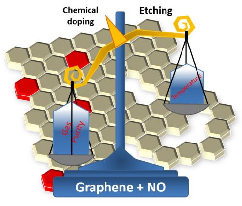
The analysis did not yield the expected results as it failed to quantify nitrogen, which was below the detection limit. However, the use of the enriched gas eventually brought great satisfaction to the team. Indeed, when the researchers compared the electronic properties of both sample types, they found that graphene treated with enriched gas always had superior properties. “Initially, such a result created much confusion in the interpretation of the results,” says Professor Radtke. “But after a few more experiments, it became one of the most important points of the article, highlighting the importance of gas purity during processing,” he adds. Specifically, the conclusion was that by properly controlling the temperature and purity of the gas during the treatment one can eliminate the problem of oxidative graphene degradation.

Thus, based on solid knowledge and scientific method, as well as some serendipity, the UFRGS team was able to develop a process of waste removal, defect neutralization and graphene doping, which improved the electronic properties of the material without producing deleterious side effects. Because it is a heat treatment in a gas atmosphere, a step that is now part of the industrial production of graphene, the process proposed by the Brazilian team could be easily applied in the production of graphene sheets for devices.

“The insertion of heteroatoms (such as nitrogen) into the graphene network without the degradation of its properties is especially important in the production of optoelectronic devices, high speed transistors, low power electronics and photovoltaic cells,” says Radtke, noting that manufacturing these graphene-based devices may be a reality in years to come. “The Graphene Flagship (European consortium of industries, universities and institutes) has announced the implementation of a pilot plant to integrate graphene at different production stages of devices as early as 2020,” comments the professor from UFRGS.

The study, which was funded by the Brazilian agencies CNPQ (mainly through INCTsNamitec and INES), Capes and Fapergs, was developed within the PhD in Microelectronics by Guilherme Koszeniewski Rolim, held at the UFRGS Graduate Program in Microelectronics and defended in 2018. The experimental work was carried out at the UFRGS Solid Surface and Interfaces Laboratory and the Brazilian National Synchrotron Light Laboratory.

[Paper: Chemical Doping and Etching of Graphene: Tuning the Effects of NO Annealing. G. K. Rolim, G. V. Soares, H. I. Boudinov, and C. Radtke. J. Phys. Chem. C,  2019, 123, 43, 26577-26582. https://doi.org/10.1021/acs.jpcc.9b02214.]

Featured paper: Controlling the electronic properties of graphene on silicon carbide.

[Paper: Graphene on the oxidized SiC surface and the impact of the metal intercalation. J.E.Padilha, R.B.Pontes, F. Crasto de Lima, R. Kagimura, R. H. Miwa. Carbon, Volume 145, April 2019, Pages 603-613.]

Controlling the electronic properties of graphene on silicon carbide

A Brazilian scientific team performed a study based on supercomputer simulations that reveals a way to overcome the challenge of controlling the electronic properties of graphene. Solutions to this challenge can make a difference in the development of two-dimensional electronic devices – a dimension in which graphene, the one-atom thick network of carbon atoms, stands out for its properties.

In fact, graphene is an extremely tough, lightweight, flexible and transparent material. It is also an excellent conductor of heat and electricity. However, it is still difficult to control the concentration and flow of electric charges in graphene, which limits its use in electronics.

Solutions have been proposed to overcome this technological limitation of graphene. Some of them are based on the insertion of small amounts of metallic atoms that modulate the electronic properties of the material without impairing the other characteristics. The method is similar to the doping of silicon, practiced routinely in the manufacture of semiconductors for the electronics industry.

Representation of the studied system: graphene sheet on substrate of oxidized silicon carbide with layer of intercalated metallic atoms (in this case, gold).

In the study that was recently reported in the scientific journal Carbon (impact factor 7,466), the Brazilian team investigated the structure and electronic properties of a graphene sheet on a silicon carbide (SiC) substrate – material often used to deposit or grow graphene. In this system, graphene remains attached to the substrate without chemical bonds, by means of distance-dependent weak attraction forces, called Van der Waals forces.

Given that in the production of graphene the presence of oxygen usually oxidizes the surface of the silicon carbide, the Brazilian scientists included in the simulations a layer of silicon oxide between the graphene and the substrate. Finally, in order to understand in detail the effect of the insertion of metallic atoms into this type of materials, the scientists added to the simulated system a layer of gold or aluminum atoms embedded in the oxide layer (in this case, Si2O5) in the interface region with graphene.

The researchers verified that the presence of the metallic layer modulates the concentration of the positive (so-called holes) and negative (the electrons) charge carriers in both the graphene sheet and Si2O5. In addition, the gold and aluminum atoms embedded in the Si2O5, which is semiconductor, induce the formation of conducting regions on the surface of this layer, in which the excess of electrons or holes is concentrated, induced by the presence of gold or aluminum, respectively. As a result, conductive channels are formed on the surface of the Si2O5, through which the charges flow.

This two-dimensional map series shows the concentrations of electrons and holes in the graphene sheet in the two graphene systems on the silicon carbide surface finished in Si [(a) and (c)] and terminated in C [(b) and ( d)]; in the presence of an aluminum monolayer [(a) and (b)] and the other containing a gold layer [(c) and (d)].
Finally, the team verified that the “doping” effect (the change in the concentration of electrons and holes) can be enhanced by the application of an external electric field, perpendicular to the interface between the graphene and the substrate.

Based on these evidences, which were obtained mainly through computational simulations based on the Density Functional Theory, the paper suggests a way to control the concentration and flow of electrical charges on graphene sheets on silicon carbide substrates. The study also shows that the system studied (graphene sheet on oxidized silicon carbide with intercalated metal layer) can be a good platform for engineering electronic properties.

“The main contribution of the study is to show an efficient way of controlling the electronic properties of graphene on a solid surface covered with a metallic layer, by applying an external electric field,” says Professor Roberto Hiroki Miwa (Federal University of Uberlândia, UFU ), corresponding author of the paper. “We show that in addition to controlling the doping level of graphene, which is fundamental for the development of electronic devices in two-dimensional (2D) systems, the presence of the metallic monolayer allows the formation of conducting channels on the surface of the silicon carbide,” he adds. According to Miwa, the study may contribute to the development of faster, more accurate sensors, transistors and other electronic devices for charge transport and signal delivery.

At the beginning the work was motivated by the interest of UFU professors Roberto Hiroki Miwa and Ricardo Kagimura in understanding the graphene/oxide interfaces at the atomic level. The focus of the study matured as the authors delved into the scientific literature. As the volume and complexity of calculations increased, the researchers included new collaborators: a physics doctoral student at UFU (Felipe David Crasto de Lima) and professors from other institutions (José Eduardo Padilha de Sousa, from the Federal University of Paraná – Jandaia do Sul campus, and Renato Borges Pontes, Federal University of Goiás).

The authors of the paper. From the left: J. E. Padilha, R. B. Pontes, F. Crasto de Lima, R. Kagimura, R. H. Miwa.

In order to perform the calculations that support the simulations, the authors used computational resources from the Brazilian National Center for High Performance Processing (CENAPD) and the SDumont supercomputer of the Brazilian National Laboratory of Scientific Computation (LNCC). The work was funded by federal agencies CNPq and CAPES and the state agency FAPEMIG (Minas Gerais).

B-MRS Newsletter. Year 6, issue 2.


logo header 400

Newsletter of the
Brazilian Materials
Research Society

Year 6, issue 2. March 7, 2019.

Featured Paper

A team of Brazilian researchers has developed a simple, clean and very efficient method to produce hydrogen. These scientists used thin films of graphene and metal nanoparticles as catalysts for a spontaneous chemical reaction that occurs between borohydride and water. The work was reported in the Journal of Materials Chemistry A. Know more.

hidrogenio_news

Featured Scientist

We interviewed Juliana Davoglio Estradioto. This 18-year-old girl holds a collection of national and international awards received for research work carried out during high school, in which she developed biodegradable materials from agro-industrial waste and created applications for them. See our interview.

juliana news

News from B-MRS Members

– Professor Sidney J. L. Ribeiro (IQ-UNESP – Campus de Araraquara), member of B-MRS, was appointed associate editor of the journal Frontiers in Chemistry – Inorganic Chemistry. Know more.

B-MRS News

– The University Chapters Program commemorates the establishment of its 9th unit, formed by a group of 15 students from different areas of the Brazilian Federal University of Pernambuco. Know more.

banner evento

XVIII B-MRS Meeting (Balneário Camboriú, SC, Brazil, September 22 – 26, 2019)

Website: www.sbpmat.org.br/18encontro/

See invitation to abstract subsmission, here.

Abstract submission. The submission of abstracts is open until April 15. Approval, modification, or rejection notifications will be sent by May 31. Final notices for abstracts needing modification will be sent by June 21. See instructions for authors, here.

Symposia. 23 symposia proposed by the international scientific community compose this edition of the event. See the symposia list, here.

Student awards. To participate in the Bernhard Gross Award, authors must submit an extended abstract by July 11 in addition to the conventional abstract. Learn more, here.

Registrations. Registration is now open. More information, here.

Venue. The meeting will be held in the delightful Balneário Camboriú (State of Santa Catarina, Brazil), at the Hotel Sibara Flat & Conventions, located in the center of the city, close to many hotels, restaurants and shops, and only 100 meters from the sea. More information, here.

Memorial lecture. The traditional Memorial Lecture Joaquim da Costa Ribeiro will be given by Professor Yvonne Primerano Mascarenhas (IFSC – USP).

Plenary lectures. Leading scientists from institutions in Germany, Italy, Spain and the United States will deliver plenary talks on cutting-edge issues at the event. There will also be a plenary session by the Brazilian scientist Antônio José Roque da Silva, director of CNPEM and the Sirius project (new Synchrotron Light Lab). Learn more about the plenary sessions, here.

Organization. The chair of the event is Professor Ivan Helmuth Bechtold (Physics Department of UFSC) and the co-chair is Professor Hugo Gallardo (Department of Chemistry of UFSC). The program committee is formed by professors Iêda dos Santos (UFPB), José Antônio Eiras (UFSCar), Marta Rosso Dotto (UFSC) and Mônica Cotta (Unicamp). Get to know all the organizers, here.

Exhibitors and sponsors. 29 companies have already confirmed their participation in the event. Those interested in sponsoring/support can contact Alexandre at the e-mail comercial@sbpmat.org.br.

Reading Tips

– By encapsulating graphene in boron nitride, scientists are able to print patterns with nanolithography, opening up possibilities to use the material in nanoelectronics (paper from Nature Nanotechnology). Know more.

– Scientists improve activity of aluminum nanocatalysts by coating them with MOFs using a strategy inspired by the natural process of wood petrification (paper by Science Advances). Know more.

– Quantum materials: Scientists confirm experimentally that topological material of atomic thickness conducts electricity at the edges, opening possibility of its use in quantum computers (paper of Science Advances). Know more.

Opportunities

– WIN Rising Star Award in Nanoscience and Nanotechnology nominations. Know more.

– Doctoral fellowship in ultra-sensitive bioelectronic transducers in Portugal. Know more.

– Invitation to organize the official International Sol-Gel Society Conference in 2021. Know more.

Events

International Workshop on Advanced Magnetic Oxides (IWAMO 2019). Aveiro (Portugal). April 15 – 17, 2019. Site.

2019 E-MRS Spring Meeting e IUMRS – ICAM. Nice (France). May 27 – 31, 2019. Site.

20th International Symposium on Intercalation Compounds (ISIC). Campinas, SP (Brazil). June 2 – 6, 2019. Site.

10th International Conference on Materials for Advanced Technologies (ICMAT 2019). Singapore. June 23 – 28, 2019. Site.

20th International Sol-Gel Conference. Saint Petersburg (Russia). August 25 – 30, 2019. Site.

YUCOMAT 2019 & WRTCS 2019. Herceg Novi (Montenegro). September 2 – 6, 2019. Site.

XVIII B-MRS Meeting. Balneário Camboriú, SC (Brazil). September 22 – 26, 2019. Site.

19th Brazilian Workshop on Semiconductor Physics. Fortaleza, CE (Brazil). November 18 – 22, 2019. Site.

Follow us on social media

You can suggest news, opportunities, events or reading tips in the materials field to be covered by B-MRS Newsletter. Write to comunicacao@sbpmat.org.br.


Featured paper: Graphene and nickel films, the best catalysts for hydrogen production.

[Paper: Nanocatalysts for hydrogen production from borohydride hydrolysis: graphene-derived thin films with Ag- and Ni-based nanoparticles. Leandro Hostert, Eduardo G. C. Neiva, Aldo J. G. Zarbin, Elisa S. Orth. J. Mater. Chem. A, 2018,6, 22226-22233. DOI 10.1039/C8TA05834B]

Graphene and nickel films, the best catalysts for hydrogen production

Thousands of vehicles powered by hydrogen gas already circulate in some regions of the world releasing only water through the exhaust pipes. As a fuel or source of energy, hydrogen is in fact an extremely clean (does not generate harmful emissions) and efficient option (it can produce more energy than any other fuel). However, pure hydrogen does not exist in nature on Earth. It needs to be produced, and most of the hydrogen-generating methods known to date have both economic and ecological drawbacks.

An alternative to these methods was recently presented by a team of researchers from the graduate program in Chemistry of the Brazilian Federal University of Paraná (UFPR). These scientists have proposed a clean, efficient, simple and inexpensive method to produce hydrogen. The team developed new catalysts (compounds that modify the speed of a chemical reaction without being consumed during the reaction), made of graphene and metal nanoparticles, which made hydrogen production feasible through the hydrolysis of borohydride – a chemical reaction still little used in hydrogen generation, notwithstanding its enormous potential as it is clean and very simple.

Photographs and representative schematics of H2 generation by hydrolysis of borohydride catalyzed with graphene and metallic nanoparticles thin films. The films, about 500 nm thick, cover the two sides of a glass plate, covering 15 cm2, which is immersed in a solution of sodium borohydride and water. The photos depict the bubbles of hydrogen gas generated on the surface of the catalyst.

In this reaction, which is performed at room temperature, sodium borohydride (NaBH4) molecules, spontaneously react with water molecules generating hydrogen (H2) molecules. The process takes place in only one step, and is performed with catalyst materials, which accelerate the reaction rate.

“The main contribution of this work is the possibility of H2 generation through thin films of graphene nanocomposites,” says Professor Elisa Souza Orth, corresponding author of an article on the work, recently published in the Journal of Materials Chemistry A (impact factor = 9,931). “Nanocomposites of carbon-based materials and metallic nanoparticles have shown many promising applications and we have shown that for the less exploited borohydride hydrolysis they could also be used efficiently,” she adds.

Among the thin film catalysts produced by the UFPR team, the ones that presented better performance were those of reduced graphene oxide with nickel nanoparticles (rGO/Ni). In fact, this nanocomposite, produced with a relatively inexpensive metal, performed better than most of the catalysts previously reported in the scientific literature, including those prepared with noble metals, which cost much more.

In general, this means that small amounts of rGO/Ni (some tens of mg) generated large volumes of hydrogen (400 ml) in a short time (5 hours).

In addition, the films developed by the Brazilian team presented another important characteristic for a catalyst: they can be easily removed from the reaction vessel, washed and dried without damage, thus allowing their reuse. “In this work, we were able to reuse the same nanocatalyst in 10 consecutive cycles, without losing activity,” says Professor Orth.

The doctoral student Leandro Hostert in the laboratory of the postgraduate program of chemistry of UFPR.
The doctoral student Leandro Hostert in a laboratory of the postgraduate program in chemistry of UFPR.

These results were made possible by combining competencies in the production of carbon nanomaterials from the Materials Chemistry Group, coordinated by Professor Aldo José Gorgatti Zarbin, with expertise in catalysis processes of the Catalysis and Kinetics Group, led by Professor Orth. These two UFPR groups have a history of collaboration in the application of carbon materials; initially, in the study of pesticides and, currently, in the development of multifunctional materials with extraordinary catalytic activity.

In addition to the development of catalysts and their application in hydrogen production, the work published in the Journal of Materials Chemistry A included an analysis of the various ways of measuring the catalytic activity of a material. The authors were able to standardize criteria and compare several results obtained in the laboratory and found in the scientific literature. “We have developed a kinetic study that complements the discussion of these complex reactions and can help guide us to a more concise understanding of catalytic activity,” explains Elisa Orth.

The research was carried out under the doctoral program in progress of Leandro Hostert, guided by Professor Orth, and was funded by Brazilian agencies CNPq, CAPES, Araucária Foundation, INCT Nanocarbono, as well as L’Oréal-UNESCO-ABC through the Award for Women in Science (2015 ) and International Rising Talents (2016) received by Elisa Orth.

Featured paper: Towards two-dimensional diamond.

Two-dimensional materials, those whose thickness goes from an atom to a few nanometers, have unique properties related to their dimensionality and are protagonists in the development of nanotechnology and nanoengineering.

A team of scientists from five Brazilian institutions and one American institution took an important step in the development of the two-dimensional diamond version. This work on 2D diamond was reported in a paper published in Nature Communications (impact factor 12,124) with open access.

“Our work presented spectroscopic evidence of the formation of a two-dimensional diamond, which we named diamondene”, says Luiz Gustavo de Oliveira Lopes Cançado, professor at the Brazilian Federal University of Minas Gerais (UFMG) and corresponding author of the paper. In choosing the name of the new material, the scientists followed the tradition of using the suffix “ene” for two-dimensional materials, as with graphene, 2D version of the graphite.

box_enIn fact, it was from the compression of graphene sheets that the diamondene was obtained by the team led by Professor Cançado. Initially, the team deposited two layers of graphene one on top of the other and transferred the graphene bilayer to a Teflon substrate, chosen for being chemically inert, preventing the formation of bonds with the graphene.

The sample of bi-layered graphene on Teflon was then subjected to high pressures and simultaneously analyzed by Raman spectroscopy at the Laboratory of Vibrational Spectroscopy and High Pressure of the Department of Physics of the Brazilian Federal University of Ceará (UFC). The experimental system used was a diamond anvil cell with a coupled Raman spectrometer. This equipment allows high pressure to be applied to small samples that are immersed in a pressure transmitting medium (in this case, water). The pressure is applied through two pieces of diamond (material chosen for being one of the hardest and resistant to compression), which compress the transmitting medium, which passes the pressure to the sample. At the same time, the spectrometer allows to monitor the changes that occur in the structure of the sample material against the different pressures applied. “In Raman spectroscopy, light behaves like a probe that measures vibrational states of the material,” explains Cançado. As a result of the probing, the spectrometer generates graphs (spectra), through which it is possible to identify the structure of the material being studied.

By analyzing the spectra, the team of scientists observed changes in the two-dimensional material that indicated the transition from a graphene structure to a diamond structure. The researchers were able to conclude that the diamondene was obtained at a pressure of 7 gigapascals (GPa), tens of thousands of times higher than the atmospheric pressure. “The evidence we present in this work is a signature in the vibrational spectrum obtained from a two-dimensional carbon material that indicates the presence of sp3 bonds, typical of the structure of the diamond,” says Professor Cançado.

To explain the formation of diamondene, the team used first principles calculations following the Density Functional Theory and Molecular Dynamics simulations. “These theoretical results guided the experiments and allowed us understanding the experimental results,” says Cançado.

Scheme of the diamondene formation mechanism from two layers of graphene submitted to high pressures (blue arrows) in water as pressure transmitting medium. The gray colored balls represent the carbon atoms; the red ones, the oxygen atoms, and the blue ones, the hydrogen atoms.

According to the theoretical results, when the bilayer graphene system on inert substrate with water as pressure transmitting medium is subjected to high pressures, the distances between the elements of the system decrease and new connections occur among them. “When applying this level of pressure on graphene, connections can change, going from the sp2 configuration to the sp3 configuration,” explains Professor Cançado. The carbon atoms in the upper graphene layer then establish covalent bonds with four neighboring atoms: the atoms of the lower layer and the chemical groups offered by water (OH- and H). The latter are fundamental to stabilize the structure. In the lower layer, in contact with the inert substrate, half of the carbon atoms are bound to only three neighboring atoms. “The pending connections give rise to a gap opening in the electronic structure, as well as polarized spin bands,” adds Cançado.

This feature makes diamondene a promising material for the development of spintronics (the emerging strain of electronics at the nanoscale in spin-bases electronics). According to Cançado, diamondene could also be used in quantum computing, microelectromechanical systems (MEMS), superconductivity, electrodes for electrochemistry-related technologies, DNA engineering substrates and biosensors – applications in which thin diamond films have already proven to have good performance.

However, there is still a long way to go before demonstrating the diamondene applications. Firstly, because the diamondene shown in the article dismantles under normal pressure conditions. To overcome this limitation, the group of Professor Cançado at UFMG is setting up an experimental system that will allow the application of much higher pressures to the samples in the order of 50 GPa and analyze them using Raman spectroscopy. “With this we intend to produce stable diamondene samples, which remain in this form even after having the pressure reduced to the level of ambient pressure,” says Cançado.

In addition, since Raman spectroscopy provides indirect evidence of the structure of the material, it will be necessary to perform direct measurements of the diamondene to know its structure in detail. “The most promising techniques in this case would be X-ray diffraction in synchrotron light sources or electron diffraction,” suggests Cançado. “The complicating factor in this experiment is the need to have the sample subjected to high pressures,” he adds.

The Brazilian history of diamondene

The idea of the 2D diamond formation originated in the doctoral research of Ana Paula Barboza, conducted under the guidance of Professor Bernardo Ruegger Almeida Neves and defended in 2012 in the Department of Physics of UFMG. In this work, Cançado says, atomic force microscopy (AFM) tips were used to apply high pressures on one, two and several layers of graphene. Indirect evidence of the formation of a two-dimensional diamond was obtained by means of electric force microscopy (EFM). The work showed the importance of the presence of two layers of graphene and water for the formation of the sp3 two-dimensional structure. The main results of the research were reported in the article Room-temperature compression induced diamondization of a few-layer graphene [Advanced Materials 23, 3014-3017 (2011)].

Main article authors. On the left, Luiz Gustavo Pimenta Martins (MSc from UFMG and doctoral student at MIT). On the right, Professor Luiz Gustavo Cançado (UFMG).

“The idea of measuring the Raman spectrum of graphene under high pressure conditions (using anvil diamond cells) came after Luiz Gustavo Pimenta Martins, an undergraduate student at the time, developed a very efficient method of transferring graphene to different substrates,” says Professor Cançado. This development was carried out during a visit to the laboratory of Professor Jing Kong at the Massachusetts Institute of Technology (MIT), after having won a grant for international mobility of the Formula Santander Award. During his master’s degree at the Physics Department of UFMG, carried out under the guidance of Professor Cançado and defended in 2015, Pimenta Martins carried out an extensive and systematic work to obtain Raman spectra of graphene samples subjected to high pressures. “There were many visits to UFC and much study until understanding the diamondene formation mechanisms,” explains Cançado.

The research reported in the Nature Communications paper was made possible by the collaborative work of several Brazilian research groups with recognized expertise in various subjects, as well as the participation of the MIT researcher in the sample preparations. Scientists from the physics departments of UFMG and UFC have contributed their recognized expertise in Raman spectroscopy applied to carbon nanomaterials and, in the case of UFC, in experiments under high pressure. Also participating in these experiments were researchers from the Brazilian Federal Institute of Education, Science and Technology of Ceará and the Brazilian Federal University of Piauí (UFPI). In addition, theoretical physicists from the Brazilian Federal University of Ouro Preto (UFOP) and UFMG performed calculations and computational simulations.

The research was funded by Brazilian federal agency CNPq, state agencies FAPEMIG and FUNCAP, Formula Santander Program and UFOP.

[Paper: Raman evidence for pressure-induced formation of diamondene. Luiz Gustavo Pimenta Martins, Matheus J. S. Matos, Alexandre R. Paschoal, Paulo T. C. Freire, Nadia F. Andrade, Acrísio L. Aguiar, Jing Kong, Bernardo R. A. Neves, Alan B. de Oliveira, Mário S.C. Mazzoni, Antonio G. Souza Filho, Luiz Gustavo Cançado. Nature Communications 8, Article number: 96 (2017). DOI:10.1038/s41467-017-00149-8. Disponível em: https://www.nature.com/articles/s41467-017-00149-8]

Featured paper: Graphene nanoflakes for a super-resistant mortar.

[Paper: Enhanced properties of cement mortars with multilayer graphene nanoparticles. Rodrigo Alves e Silva, Paulo de Castro Guetti, Mário Sérgio da Luz, Francisco Rouxinol, Rogério Valentim Gelamo. Construction and Building Materials. Volume 149, 15. September 2017, pages 378-385. https://doi.org/10.1016/j.conbuildmat.2017.05.146]

Graphene nanoflakes for a super-resistant mortar

Scanning electron microscopy image of the reinforced mortar sample. In the center of the image, some multilayer graphene nanoflakes.

Researchers from Brazilian institutions added nanometric graphene flakes to cement mortar and obtained a composite with resistance of almost 150% higher than that of conventional mortar. By means of simpler, faster and cheaper processes than previously reported in the scientific literature, the team created a reinforced mortar ready for use in civil construction. The work was reported in a paper that has just been published in a journal of the Elsevier publishing house dedicated to investigation and innovative use of materials in construction and repair, Construction and Building Materials (impact factor: 3.169).

Compared to traditional mortar, the new graphene-reinforced mortar can be used in smaller amounts and is less likely to crack over time, explains Professor Rogério Valentim Gelamo, the corresponding author of the article. Moreover, its manufacturing process poses no health or environmental risks and no further procedure is required for its complete handling and application.

Professor Gelamo believes that the powder-based multilayer graphene nanoflakes could be sold in ampoules with the required quantity to be added to 1 cubic meter of mortar. The reinforced mortar would cost around U$ 5 more per cubic meter. “The cost is really low and it could be applied or marketed by a company interested in this, since the large-scale manufacturing is already proficient in our Laboratory of Thin Films and Plasma Processes of the Federal University of Triângulo Mineiro (UFTM) in the city of Uberaba” declares Professor Gelamo.

The idea of this work came about when Gelamo decided to look for applications for the multilayer graphene he had developed during his post-doctorate at the Center for Semiconductor Components from the State University of Campinas (Unicamp), along with Francisco Rouxinol, also a postdoc. The material and its process have already been the object of papers and a patent. In 2010, Gelamo became adjunct professor of the newly created Institute of Technological and Exact Sciences at UFTM.  There, teaching in the first Civil Engineering course, Professor Gelamo met the undergraduate student Rodrigo Alves e Silva, who was enthusiastic with the idea of using multilayer graphene in the mortar. Another professor of UFTM, Paulo Guetti, joined them. “Together we carried out the first experiments with these composites, which to our surprise gave excellent results in the first tests,” recalls Professor Gelamo.

The multilayer graphene was obtained from graphite flakes donated by the Brazilian National Grafite company. Using isopropyl alcohol the researchers extracted nanoflakes formed by a maximum of 40 superimposed graphene layers, each one an atom thick, with total thickness of 0.7 nm to 20 nm. The result: multilayer graphene nanoflakes with almost no defects, in the form of powder ready to be dispersed in the mortar. The underlying idea of our work was to use graphene multilayers obtained by simpler, faster and cheaper processes than those used to obtain oxidized and chemically reduced graphene. This enabled to combine practicality and economy with the excellent thermal and mechanical properties of the graphene layers,” says Gelamo. “The way graphene is currently obtained (Hammer or similar method) creates many defects in the graphene structure, which ends up compromising its properties,” he adds.

In the second step, the scientists prepared mortar with the conventional water, cement and sand ratio, and reinforced it with five different percentages of multilayer graphene nanoflakes, ranging from 0% (mortar without graphene) to 0.033%.  “Our dispersion was also performed in an innovative and simple way, using only organic solvents mixed directly on the still dry mortar composite,” reports Professor Gelamo. The team was then able to obtain a mixture without the graphene agglomerations that are cited in most articles on cement and graphene composites.

With the five types of mortar, the team prepared cylindrical samples 5 cm in diameter and 10 cm long and tested their compressive and tensile strengths. The tests were performed 3, 7, and 28 days after the mortar preparation, following the respective standards of the Brazilian Association of Technical Standards (ABNT). All tests showed significant increases in mortar strength when reinforced with the multilayer graphene. In particular, the best tensile strength test result was obtained with samples containing the highest percentage of graphene, 7 days after its manufacture: 144.4% increase in strength compared to conventional mortar samples. As for the compressive strength, the best result (an increase of 95.7%) was achieved with the addition of 0.021% of multilayer graphene, 28 days after the mortar preparation.

The morphology and composition of the samples and the materials used in their manufacture were analyzed using several techniques. These analyses helped the team understand why adding multilayer graphene nanoflakes resulted in such significant mortar strength increases. According to the authors of the article, the presence of this graphene accelerates the hydration reaction of the mortar, generating changes in its structure and composition which in turn improve the propagation of internal stresses through the material, thereby helping to prevent the occurrence of cracks.

Notwithstanding the success obtained by applying the multilayer graphene in the mortar, Professor Gelamo continues looking for other applications for his graphene nanoflakes through partnerships with Brazilian and international groups. “We have used multi-layer graphene in field-emitting devices, batteries, flexible and self-supporting supercapacitors, chemical and biological sensors, nanofluids for machining, and other applications,” he says. “We have also functionalized the graphene multilayers with reactive plasmas in order to change the properties of these materials, with some works already published,” he adds.

The research that originated the Construction and Building Materials article was carried out with financial support from Brazilian agencies CNPq, Capes and Fapemig.

The authors of the paper. From the left, Rodrigo Alves e Silva (UFTM), Paulo de Castro Guetti (UFTM), Mário Sergio da Luz (UFTM), Francisco Paulo Rouxinol (Unicamp) and Rogério Valentim Gelamo (UFTM).
The authors of the paper. From the left, Rodrigo Alves e Silva (UFTM), Paulo de Castro Guetti (UFTM), Mário Sergio da Luz (UFTM), Francisco Paulo Rouxinol (Unicamp), and Rogério Valentim Gelamo (UFTM).

Featured paper: Nanosheets and nanoparticles interconnected for wearable electronics.

[Paper: Self-Assembled and One-Step Synthesis of Interconnected 3D Network of Fe3O4/Reduced Graphene Oxide Nanosheets Hybrid for High-Performance Supercapacitor Electrode. Rajesh Kumar, Rajesh K. Singh, Alfredo R. Vaz, Raluca Savu, Stanislav A Moshkalev. ACS APPLIED MATERIALS & INTERFACES. 2017, 9, 8880 – 8890. DOI: 10.1021/acsami.6b14704].

Nanosheets and nanoparticles interconnected for wearable electronics

A team of researchers from the State University of Campinas (Unicamp), in Brazil, and a researcher from the Central University of Himachal Pradesh (CUHP), in India, have developed a flexible and tiny high-performance supercapacitor with a hybrid material made of graphene oxide (GO) nanosheets and iron oxide (Fe3O4) nanoparticles. The work was recently reported in the journal Applied Materials & Interfaces (impact factor 7.145), of the American Chemical Society.

“The main contribution of this work is for the new and really promising research area of flexible electronics”, says PhD Rajesh Kumar, researcher at Unicamp’s Center for Semiconductor Components (CSC) and corresponding author of the article. “Since capacitors are among the main components of electronic devices, these performant and flexible graphene oxide-based microsupercapacitors can be used in the near future as components in wearable and flexible electronic devices (mobile phones, smart watches, health monitoring devices, energy storage devices etc.)”, adds the Indian born researcher.

The genesis of the study goes back to 2015, when Rajesh Kumar, who had been working with graphene microsupercapacitors in other countries, applied for a postdoctoral fellowship to work in the group of Professor Stanislav Moshkalev, director of CSC at Unicamp. “I saw a great opportunity in this group, as their main research line is nanofabrication and nanoelectronics based on nanostructured carbon,” reports Kumar. The Indian PhD obtained a grant from CNPq, the Brazilian federal research agency, as a visiting specialist, to carry out a project in CSC – Unicamp. Initially, he made fine sheets of graphene oxide called “buckypapers”. Then, working in interaction with a group of five other people of CSC – Unicamp, he searched for new strategies to improve the properties of the material.

The CSC- Unicamp team thus faced the challenge of making a hybrid material of graphene and iron oxide with controlled structure using a simple process, and it was successful in do so by simply exposing graphite oxide and ferric chloride (FeCl3) to microwave radiation.

SEM image of the 3D hybrid material Fe3O4/rGO (left), and a representative scheme of the material´s morphology (right).

The obtained material presented an interesting morphology: a three-dimensional network in which interconnected graphene nanosheets form “tunnels” that harbor crystalline and multifaceted iron oxide nanoparticles of 50 – 200 nm, strongly attached to the nanosheets, as shown in the figure beside.

The morphology, structure, composition, thermal stability and other properties were analyzed using several techniques available at CSC – Unicamp and at the Indian university.

Subsequently, at Unicamp, the team tested the efficiency of the material to act as electricity storage. The tests proved the high performance of the material as a supercapacitor electrode, and the scientific team concluded that this efficiency was favored by the special morphology of the 3D hybrid material. Particularly, by the faceted nanoparticles strongly attached to the nanosheets, the separation among the nanosheets, the “tunnels” that shelter individual nanoparticles avoiding agglomerations, and the large surface area of the network of nanosheets.

“These microsupercapacitors can and for sure will, in the near future, replace the traditional capacitors in electronic devices,” says Kumar. According to the researcher, their main advantages are high performance, mechanical strength, reduced size and, most important, flexibility – an essential property for wearable electronics.

In addition, the method developed by the Unicamp and CUHP team can become a good alternative to fabricate other hybrid materials based on carbon and metal oxides.

The work was carried out with financial support from CNPq and FAPESP (the São Paulo State research foundation).

Pictures of the authors of the paper. From the readers´ left, Rajesh Kumar (Unicamp), Rajesh Kumar Singh (CUHP), Alfredo Vaz (Unicamp), Raluca Savu (Unicamp), and Stanislav Moshkalev (Unicamp).

Featured paper: Advanced material for ultra-capacity supercapacitors.

[Paper: One-step electrodeposited 3D-ternary composite of zirconia nanoparticles, rGO and polypyrrole with enhanced supercapacitor performance. Alves, Ana Paula P.; Koizumi, Ryota; Samanta, Atanu; Machado, Leonardo D.; Singh, Abhisek K.; Galvao, Douglas S.; Silva, Glaura G.; Tiwary, Chandra S.; Ajayan, Pulickel M. NANO ENERGY, volume 31, January 2017, 225–232. DOI: 10.1016/j.nanoen.2016.11.018.]

Advanced material for ultra-capacity supercapacitors.

Supercapacitors are electrical storage devices with a particular feature of releasing large amounts of energy in a short time interval. They are already used, for example, in electric or hybrid vehicles, camera flashes and elevators, but they can still be improved – largely with the contribution of Materials Science and Technology – for current and potential applications. Putting it simply, a supercapacitor consists of two electrodes, positive and negative, separated by a substance containing positive and negative ions (the electrolyte).

An article recently published in the scientific journal Nano Energy (Impact Factor 11,553) reports on a contribution from an international and interdisciplinary scientific team to develop materials that improve the performance of supercapacitors. Using a simple and easily scalable process, the team of researchers from Brazil, the United States and India produced electrodes made of a composite material composed of polypyrrole (PPi), reduced graphene oxide (rGO) and zirconium oxide (ZrO2) nanoparticles. By combining the three materials, the scientists were able to generate a large surface area and high porosity electrode – basic characteristics to promote the interaction of the electrolyte ions with the surface of the electrodes and therefore enhance the performance of the supercapacitor.

“Our unique contribution was the synthesis, in a single and simple stage of electrodeposition, of a hybrid containing graphene, zirconium oxide and polypyrrole, and the experimental demonstration of considerable gains in electrochemical properties, parallel to the theoretical modeling in order to understand the role of the components of the material”, states Glaura Goulart Silva, professor in the Department of Chemistry at the Federal University of Minas Gerais (UFMG) and a corresponding author of the paper.

In addition to preparing samples of the ternary (i.e., composed of three elements) composite PPi/rGO/ZrO2, using the same method for comparison purposes, the team prepared samples of the PPi/rGO binary composite, and pure polypyrrole samples. The three materials were analyzed using XPS (spectroscopy of X-ray excited photoelectrons), SEM (Scanning Electron Microscopy), Raman spectroscopy and transmission electron microscopy to determine their composition, structure and morphology.

As seen in the SEM images of the figure below, the scientists noted that the addition of graphene oxide and zirconia nanoparticles significantly changed the morphology of the material. While the pure polypyrrole had formed a cracked, wire-like film, the graphene composite had a granular morphology, with no cracks, and the zirconium oxide material had a leaf-like appearance.

At the end of the experimental stage of the study, the scientists performed a series of tests to measure the performance of the three materials as supercapacitors. The results showed that the capacity to store electrical charges (capacitance) had increased up to 100% in the ternary composite with respect to the polypyrrole. Moreover, instead of decreasing this performance due to the use of the electrode, it increased by 5% after 1,000 recharges in the binary and ternary composites.

This was the first paper that presented the introduction of zirconium oxide nanoparticles in polypyrrole and graphene electrodes for supercapacitors. Therefore, the team performed computational modeling to analyze the role of zirconium oxide in the performance of the composite. The simulations confirmed the beneficial effects of the nanoparticles on the stability of the material, directly related to extending the life of the electrodes.

Illustrative diagram of charge storage and interaction of ions near the surface of pure polypyrrole electrodes (PPi), reduced graphene oxide (PPi/rGO) and polypyrrole PPi/rGO/ZrO2 (above), based on the morphology associated with the SEM images of the surface of the electrodes with the respective materials under carbon fiber substrate (below). Image by Ana Paula Pereira Alves for her PhD thesis.
Above, illustrative diagram of charge storage and interaction of ions near the surface of pure PPi electrodes, PPi/rGO electrodes, and PPi/rGO/ZrO2 electrodes, based on the morphology associated with the SEM images of the surface of the electrodes with the respective materials under carbon fiber substrate (below). Image by Ana Paula Pereira Alves for her PhD thesis.

“There is great potential in the application of these new composites in supercapacitors due to the need to increase the energy density provided by the device, in parallel with its miniaturization,”declares Professor Goulart Silva. “The alternative developed in the work in question allows better performance in terms of cycling stability with gains in the safety of the supercapacitor. The use of supercapacitors and batteries in electric and hybrid cars is one of the technological fronts where these materials can be applied,” she adds.

From the reader's left: Professor Glaura Goulart Silva (UFMG), Professor Pulickel Ajayan (Rice University) and Ana Paula Pereira Alves, a recently graduated doctor from UFMG.
From the reader’s left: Professor Glaura Goulart Silva (UFMG), Professor Pulickel Ajayan (Rice University) and Ana Paula Pereira Alves, a recently graduated doctor from UFMG.

The work is part of the doctorate in Chemistry of Ana Paula Pereira Alves, conducted with the guidance of Professor Goulart Silva and defended in February of this year at UFMG with a thesis about synthesis and characterization of advanced materials for supercapacitors. During her doctoral work at the University of Minas Gerais, Pereira Alves carried out intensive training in synthesis techniques and physical-chemical analysis of conjugated polymers and graphene and in the characterization of supercapacitors. In 2015, she went to the United States for a one-year “sandwich” internship, with the support of the National Council for Scientific and Technological Development (CNPq), in the Department of Materials Science and Nanoengineering at Rice University, in the research group of Professor Pulickel Ajayan (researcher with h=139 index according to Google Scholar), who has collaborated with Professor Goulart Silva’s group since 2010. “Professor Ajayan has systematically proposed radical innovations in synthesis and design of batteries and supercapacitors, with significant international impact in the area,” she adds.

The experimental work reported in the paper was carried out at Rice University, with the presence of all authors, including those from Brazil and India, and also Professor Goulart Silva, who was there in February 2016, with the support of Minas Gerais Research Foundation (Fapemig). “The highly interdisciplinary environment of the Department of Materials Science and NanoEngineering at Rice made possible for the engineers, physicists, and chemists to come together to work on a current major problem.”, says Goulart Silva.

The computational modeling was carried out by Brazilian researchers from the State University of Campinas (Unicamp) and the Federal University of Rio Grande do Norte (UFRN) –among them Professor Douglas Galvão (Unicamp), who has maintained a scientific collaboration with Professor Ajayan since before the beginning of this research.

“I consider this work to be an excellent example of success, where the competence of the Brazilian groups joined that of a highly productive and impactful group in the international scenario and complement each other,” declares Goulart Silva. “The stability and increase of investments in research and development in Brazil are essential for endeavors as this to be widespread. Research is an investment that needs to be done over the long term, without setbacks, to enable a high rate of return in terms of materials, technologies and highly qualified people. Ana Paula Alves is now a young doctor in search of the opportunity to put together her research group and hence train new students and hence contribute to face the challenges of our country,” reaffirms Goulart Silva.

Featured paper. A lot of science and some serendipity to discover the recipe for a multifunctional nanocomposite.

[Paper: One material, multiple functions: graphene/Ni(OH)2 thin films applied in batteries, electrochromism and sensors. Eduardo G. C. Neiva, Marcela M. Oliveira, Márcio F. Bergamini, Luiz H. Marcolino Jr & Aldo J. G. Zarbin. Scientific Reports 6, 33806 (2016). doi:10.1038/srep33806. Link para o artigo: http://www.nature.com/articles/srep33806]

A lot of science and some serendipity to discover the recipe for a multifunctional nanocomposite.

boxnickel_enA recently published paper in the journal Scientific Reports, from the Nature group, reports a study carried out in universities of the state of Paraná (Brazil) on a material based on nickel hydroxide Ni(OH)2 – a composite of great technological interest [See box]. The group of authors developed an innovative method to fabricate a material based on nickel hydroxide graphene and nanoparticles, prepared thin films with this material and demonstrated the efficiency of these films when used as rechargeable battery electrodes, glycerol sensors and electrochromic materials.

The work was carried out within the doctoral research of Eduardo Guilherme Cividini Neiva, under the guidance of Professor Aldo José Gorgatti Zarbin, in the Chemistry Post-Graduation Program of the Federal University of Paraná (UFPR). Neiva began his research on nickel nanoparticles during his undergraduate years, guided by Professor Zarbin. In the master’s program, still with Zarbin, he developed a preparation route of nickel metal nanoparticles for electrochemical applications. After completing the master’s program, Neiva and Zarbin set out to continue the research in Neiva’s doctorate, including graphene in the preparation of nickel metal based nanoparticles to obtain nickel and graphene nanocomposites with different properties. “Most of my scientific interests focus on the preparation of materials with carbon nanostructures, such as nanotubes and graphene,” states Professor Zarbin, who is the corresponding author of the article in Scientific Reports.

They were surprised by the first laboratory results. In the presence of graphene oxide (as a precursor of graphene in the preparation of the material), the process took a different course. At that time, Neiva and Zarbin saw the potential of these particularities: if well understood, they could be controlled and used to prepare nanocomposites, not only of nickel metal, but also of nickel hydroxide, which would open up new application possibilities. “There is a phrase by Louis Pasteur I like very much, which applies perfectly in this case: “Chance favors the prepared mind,” declares Zarbin.

Based on this, student and advisor created a simple and direct process for the fabrication of graphene and nickel hydroxide nanocomposites. In this innovative process, both components are synthesized together in a one-step reaction. Using this technique, Neiva manufactured the nanocomposites. Pure nickel hydroxide samples were also produced in order to compare them with the nanocomposites.

The samples were studied through a series of techniques: X-ray diffraction, Raman spectroscopy, Fourier transform infrared spectroscopy (FT-IR), thermogravimetry, field emission scanning electron microscope (FEG-MEV), and also by means of transmission electron microscopy (TEM) images carried out by Professor Marcela Mohallem Oliveira, from the Federal Technological University of Paraná (UTFPR). The comparison between the two materials was favorable to the nanocomposite. “Graphene played a key role in the stabilization of particles at the nanometer scale, increasing the chemical and electrochemical stability of the nanoparticles, and increasing the conductivity of the material, which is fundamental for an improvement in the desired applications,” acknowledges Aldo Zarbin.

Aldo José Gorgatti Zarbin (on the left side) and Eduardo Guilherme Cividini Neiva, the main authors of the paper, standing at the FEG-MEV equipment of the Materials Chemistry Group of UFPR.

The next stage consisted of

processing the nanocomposites and the nanoparticles of pure nickel hydroxide to obtain thin films, a format that allows using them in the desired applications. “The deposition of materials in the form of films, covering different surfaces, is a great technological challenge, even greater when dealing with multicomponent materials and insoluble, infusible and intractable materials (all characteristics of the material reported in this article)”, explains Zarbin.

To overcome this challenge, Neiva used a processing route, known as liquid/liquid interfacial method, developed in 2010 by the research group led by Zarbin, the Materials Chemistry Group of UFPR. This route, besides simple and cheap, explains Professor Zarbin, allows depositing complex materials in the form of homogeneous and transparent films on various types of materials, including plastics. “The route is based on the high energy at the interface of two immiscible liquids (e.g., water and oil), where the material is initially stabilized to minimize this energy, allowing its subsequent transfer to substrates of interest,” he explained.

With the nanocomposites, Neiva obtained thin transparent films of about 100 to 500 nm in thickness, with nanoparticles of about 5 nm in diameter, distributed homogeneously on the graphene sheets. The pure nickel hydroxide, however, generated films formed by porous spherical nanoparticles of 30 to 80 nm in diameter, distributed heterogeneously, forming agglomerates in some regions.

In the final phase of the work, the films deposited on glass and indium tin oxide were tested in three applications, in which the nanocomposite performed better than pure nickel hydroxide.  As a material for rechargeable alkaline battery electrodes, the nanocomposite exhibited high energy and high power – two positive points that are not easily found in the same material. The nanocomposite also showed good performance as an electrochemical sensor. In fact, experiments designed by Professors Márcio Bergamini and Luiz Marcolino Jr, also from UFPR, showed that the nanocomposite is a sensitive sensor of glycerol (a compound known commercially as glycerin and used in several industries). Finally, the nanocomposite acted as an efficient electrochromic material. With these characteristics, the films of the UFPR group have a chance to leave the laboratory and be part of innovative products. “This depends on partners who are interested in scaling the method and testing it on real devices,” says Zarbin.

For now, in addition to scientific articles such as the one published in the journal Scientific Reports, the work generated several patents, both on the deposition method of thin films and on their applications in gas sensors, transparent electrodes, photovoltaic devices and catalysts. “And we have now developed a flexible battery, which was only possible thanks to the film deposition technique we developed,”, adds Professor Zarbin.

The work, which was developed within the macro projects “INCT of carbon nanomaterials” and “Nucleus of Excellence in Nanochemistry and Nanomaterials”, received funding from the federal agencies Capes and CNPq, and the Araucária Foundation, an agency for scientific and technological development of the state of Paraná.

This figure, sent by the authors of the paper, summarizes the main contributions of the paper. In the center, a flask with two liquids and the film at the interface represents the processing method of thin films. A diagram of the film is on the left, with the nickel hydroxide nanoparticles on the graphene sheet. To the right, a photograph of the film deposited on a quartz substrate shows the homogeneity and transparency of the film (it is possible to read text below it). And to the right, from top to bottom, the three applications are shown by a discharge curve (battery), of a transmittance variation curve by the applied potential (electrochromism) and an analytical curve showing the linear variation of the intensity of the current as a function of glycerol concentration in the medium (sensor).
This figure, sent by the authors of the paper, summarizes the main contributions of the paper. In the center, a flask with two liquids and the film at the interface represents the method for thin films processing. A diagram of the film is on the left, with the nickel hydroxide nanoparticles on the graphene sheet. To the right, a photograph of the film deposited on a quartz substrate shows the homogeneity and transparency of the film (it is possible to read text below it). And to the right, from top to bottom, the three applications are shown by a discharge curve (battery), of a transmittance variation curve by the applied potential (electrochromism) and an analytical curve showing the linear variation of the intensity of the current as a function of glycerol concentration in the medium (sensor).