Featured paper: Graphene and nickel films, the best catalysts for hydrogen production.

[Paper: Nanocatalysts for hydrogen production from borohydride hydrolysis: graphene-derived thin films with Ag- and Ni-based nanoparticles. Leandro Hostert, Eduardo G. C. Neiva, Aldo J. G. Zarbin, Elisa S. Orth. J. Mater. Chem. A, 2018,6, 22226-22233. DOI 10.1039/C8TA05834B]

Graphene and nickel films, the best catalysts for hydrogen production

Thousands of vehicles powered by hydrogen gas already circulate in some regions of the world releasing only water through the exhaust pipes. As a fuel or source of energy, hydrogen is in fact an extremely clean (does not generate harmful emissions) and efficient option (it can produce more energy than any other fuel). However, pure hydrogen does not exist in nature on Earth. It needs to be produced, and most of the hydrogen-generating methods known to date have both economic and ecological drawbacks.

An alternative to these methods was recently presented by a team of researchers from the graduate program in Chemistry of the Brazilian Federal University of Paraná (UFPR). These scientists have proposed a clean, efficient, simple and inexpensive method to produce hydrogen. The team developed new catalysts (compounds that modify the speed of a chemical reaction without being consumed during the reaction), made of graphene and metal nanoparticles, which made hydrogen production feasible through the hydrolysis of borohydride – a chemical reaction still little used in hydrogen generation, notwithstanding its enormous potential as it is clean and very simple.

Photographs and representative schematics of H2 generation by hydrolysis of borohydride catalyzed with graphene and metallic nanoparticles thin films. The films, about 500 nm thick, cover the two sides of a glass plate, covering 15 cm2, which is immersed in a solution of sodium borohydride and water. The photos depict the bubbles of hydrogen gas generated on the surface of the catalyst.

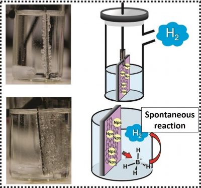
In this reaction, which is performed at room temperature, sodium borohydride (NaBH4) molecules, spontaneously react with water molecules generating hydrogen (H2) molecules. The process takes place in only one step, and is performed with catalyst materials, which accelerate the reaction rate.

“The main contribution of this work is the possibility of H2 generation through thin films of graphene nanocomposites,” says Professor Elisa Souza Orth, corresponding author of an article on the work, recently published in the Journal of Materials Chemistry A (impact factor = 9,931). “Nanocomposites of carbon-based materials and metallic nanoparticles have shown many promising applications and we have shown that for the less exploited borohydride hydrolysis they could also be used efficiently,” she adds.

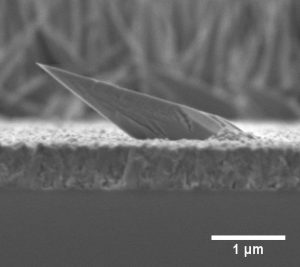
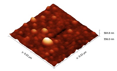
Among the thin film catalysts produced by the UFPR team, the ones that presented better performance were those of reduced graphene oxide with nickel nanoparticles (rGO/Ni). In fact, this nanocomposite, produced with a relatively inexpensive metal, performed better than most of the catalysts previously reported in the scientific literature, including those prepared with noble metals, which cost much more.

In general, this means that small amounts of rGO/Ni (some tens of mg) generated large volumes of hydrogen (400 ml) in a short time (5 hours).

In addition, the films developed by the Brazilian team presented another important characteristic for a catalyst: they can be easily removed from the reaction vessel, washed and dried without damage, thus allowing their reuse. “In this work, we were able to reuse the same nanocatalyst in 10 consecutive cycles, without losing activity,” says Professor Orth.

The doctoral student Leandro Hostert in the laboratory of the postgraduate program of chemistry of UFPR.
The doctoral student Leandro Hostert in a laboratory of the postgraduate program in chemistry of UFPR.

These results were made possible by combining competencies in the production of carbon nanomaterials from the Materials Chemistry Group, coordinated by Professor Aldo José Gorgatti Zarbin, with expertise in catalysis processes of the Catalysis and Kinetics Group, led by Professor Orth. These two UFPR groups have a history of collaboration in the application of carbon materials; initially, in the study of pesticides and, currently, in the development of multifunctional materials with extraordinary catalytic activity.

In addition to the development of catalysts and their application in hydrogen production, the work published in the Journal of Materials Chemistry A included an analysis of the various ways of measuring the catalytic activity of a material. The authors were able to standardize criteria and compare several results obtained in the laboratory and found in the scientific literature. “We have developed a kinetic study that complements the discussion of these complex reactions and can help guide us to a more concise understanding of catalytic activity,” explains Elisa Orth.

The research was carried out under the doctoral program in progress of Leandro Hostert, guided by Professor Orth, and was funded by Brazilian agencies CNPq, CAPES, Araucária Foundation, INCT Nanocarbono, as well as L’Oréal-UNESCO-ABC through the Award for Women in Science (2015 ) and International Rising Talents (2016) received by Elisa Orth.

Featured paper: Moving nanoparticles for asymmetric nanowires.

[Exploring Au Droplet Motion in Nanowire Growth: A Simple Route toward Asymmetric GaP Morphologies. Bruno C. da Silva*, Douglas S. Oliveira, Fernando Iikawa, Odilon D. D. Couto Jr., Jefferson Bettini, Luiz F. Zagonel, and Mônica A. Cotta*. Nano Lett., 2017, 17 (12), pp 7274–7282. DOI: 10.1021/acs.nanolett.7b02770]

Moving nanoparticles for asymmetric nanowires.

Scanning electron microscopy image of asymmetric gallium phosphide (GaP) nanowires.

A team of scientists presented a route to grow semiconductor nanowires having an asymmetric morphology, different from the traditional cylindrical one. The possibility of producing, in a controlled manner, nanowires with particular formats and without defects, can be exploited in several applications, including the production of more efficient solar cells.

The research was led by scientists from the Brazilian university UNICAMP and the Brazilian Nanotechnology National Laboratory (LNNANO), who reported their findings in a paper in NanoLetters.

The researchers discovered the process while studying the production of nanowires of gallium phosphide (GaP) for optoelectronic applications. The team chose to produce the nanowires by chemical beam epitaxy (CBE), preceded by a thermal treatment (annealing). In this technique, a substrate of a suitable material – in this case gallium arsenide (GaAs) – is placed inside a chamber. Then, chemical compounds in the form of vapor are introduced into the chamber. Some elements of the vapored material deposit over the substrate, layer upon layer, generating films. To promote the growth of nanowires instead of films, metallic nanoparticles (in this case, gold nanoparticles) are placed on the substrate before being exposed to vapor. During exposure, these catalytic nanoparticles cause the material to deposit preferentially underneath them, causing wire-like structures to grow.

While the researchers were analyzing the nanowires they had obtained in the first few months of the work, they found a significant amount of asymmetric nanostructures. “Besides having a particular morphology, we saw that these nanowires had an hexagonal crystal structure (wurtzite) and a very low density of crystallographic defects, which motivated us to study in detail the causes for the formation of this unusual structure,” says Bruno da Silva, PhD student at UNICAMP and corresponding author of the paper.

Da Silva and his supervisor Prof. Mônica Cotta then began to raise and test hypotheses for the cause behind the formation of the peculiar structures. After several experiments and analyses, they focused on a phenomenon that caught their attention: in the early stages of the process, the gold nanoparticles spontaneously moved over the substrate. Hence, the duo undertook a systematic work on heating substrates with nanoparticle catalysts, growing nanowires under various conditions, and analyzing the resulting samples through scanning and transmission electron microscopes and atomic force microscopy.

Atomic force microscopy image of a gold nanoparticle on GaAs substrate showing the trail left by its movement.

Da Silva, Prof. Cotta and their collaborators from UNICAMP and LNNano were able to find out why the growth process they used resulted in asymmetric nanowires. The main reason was the movement of the gold nanoparticles, which was thermally activated with the initial annealing. Based on that discovery, the team established a recipe for producing asymmetric semiconductor nanowires in a controlled manner. “Our work was the first to show that the mechanical instability of the nanoparticle catalyst can be used to modify the growth of semiconductor nanowires, in our case, particularly affecting their morphology,” says Bruno da Silva.

The mechanism of the asymmetric nanowires growth presented in the NanoLetters paper can be described as follow. When heated together with the substrate, the nanoparticles begin to crawl and advance through the substrate while consuming the oxide layer that naturally covers the gallium arsenide. Thus, the nanoparticles form asymmetric grooves a few nanometers deep and a few hundred nanometers long. These trails become fertile ground for the growth of the nanowires, since the deposition rate of the vapored material is greater there than in the rest of the substrate, which is covered by the oxide. A pedestal then forms along the grooves and the nanowire grows on top of the pedestal with an asymmetrical format.  “We showed that the movement of the particle generates a zone of preferential deposition, and that the combination of this phenomenon with the axial growth “vapor – liquid – solid” leads to the asymmetry in the nanowire,” summarizes da Silva.

Besides describing the formation mechanism of asymmetric nanowires, the work of the Brazilian team generated detailed knowledge about the movement of heated metallic nanoparticles. “We have shown that in addition to temperature, vacuum conditions and surface quality of the substrate are crucial for nanoparticle stability, and that the motion direction is related to the asymmetry of gold dissolution on semiconductor surfaces III-V,” details the doctorate student.

Concerning possible applications, the asymmetry of these nanowires can be explored, for example, in the construction of antireflective layers that reduce the amount of light lost by reflection in solar cells.  Another possibility would be to exploit the green emission of these wurtzite gallium phosphide nanowire in lighting devices. Or, why not, to develop an alternative process to electronic litography taking advantage of the gold nanoparticles movement and the trails it forms on the substrate.

The work was funded by Unicamp, the Brazilian federal agencies CNPq and CAPES and the São Paulo Research Foundation (FAPESP).