Featured scientist: Edson Roberto Leite.

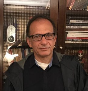
Prof Edson Roberto Leite

Edson Roberto Leite memories related to science are all very pleasant: the book about rockets in his childhood in the interior of São Paulo, the opportunity to use an exceptional microscope during the sabbatical period in the United States, the discovery of a mechanism for the growth of nanocrystals at the Brazilian National Synchrotron Light Laboratory…

Some of these wonderful memories include the many occasions experienced alongside his tutor and scientific father, Professor José Arana Varela, a prominent Brazilian materials scientist who died in 2016. Arana Varela was honored by B-MRS with the creation, in 2019, of an award that bears his name, and which annually distinguishes a prominent researcher from Brazil, who gives a plenary lecture at the Society’s annual event. In its first edition, the award was befittingly granted to Edson Roberto Leite, professor at the Federal University of São Carlos (UFSCar) and scientific director of the Brazilian National Nanotechnology Laboratory (LNNano-CNPEM). Leite is also editor for Latin America of the Journal of Nanoparticle Research (Springer).

Edson Roberto Leite received his first degree in Materials Engineering from UFSCar in 1988. In doubt between pursuing a career in industry or academia, he initially tried to reconcile both. After graduating, he worked in the research and development area at 3M, while doing his master’s degree and starting his doctorate, both in Materials Science and Engineering at UFSCar. In 1992, he left the company in order to dedicate his time to the doctorate, a decision that he recalls did not please his father-in-law, who was concerned with the livelihood of the family that by now included two children. However, over the years, the results of this decision have been very positive. In 1994, shortly after defending his doctorate, Leite became a professor in the Chemistry Department at UFSCar and started a career as a researcher in materials, which would not only be fruitful, but also enjoyable.

Co-author of more than 400 scientific articles published with more than 19 thousand citations, today Leite has an h index of 72 (Google Scholar). The scientist is also the editor of three books related to materials for energy and co-author of a book on the process of nucleation and growth of nanocrystals. Leite received several awards, including the Scopus Prize from Elsevier/CAPES (2006), for the excellence of his scientific production as a whole, and the John Simon Guggenheim Memorial Foundation Fellowship (2009), awarded to scientists with exceptional research skills. In 2012, Edson Leite was elected member of the World Academy of Ceramics and the Academy of Sciences of the State of São Paulo. In 2014, he was cochair of the Spring Meeting of Materials Research Society, held in San Frascisco (USA). In 2019 he was elected full member of the Brazilian Academy of Sciences (ABC).

Read our interview and learn more about this scientist, his main contributions and his memories of Professor Arana Varela.

B-MRS newsletter: At school, you had more affinity with science subjects, right? Do you remember how this taste for science originated?

Edson Roberto Leite: A person’s story always has the personal version and the version of the people who interacted with him. I will recount my perspective of how it happened.

At school I always had a strong affinity for Science and History. A striking memory was when I was in the third grade of elementary school and my father took me to the Municipal Library of Araras to take out a membership card so I could access books. The first book I chose was about rockets. I have always loved the conquest of space and the science behind fundamental historical moments. It is noteworthy that man had reached the moon only a few years earlier, nuclear power was seen as the global energy solution and semiconductors were just beginning.

In addition to this fond memory, there were other motivations, including Jonny Quest, a really cool cartoon. This animation, in addition to the adventures, had a lot of science fiction, and Jonny’s father (Dr. Benton Quest) was a renowned scientist with an excellent research laboratory in his own home.

My childhood, then, was always marked by a strong influence of science classes. I think it easily guided me to choose Engineering. At first the idea was to become a mechanical engineer, but during my prep course for the entrance exam I was introduced to Materials Engineering, at UFSCar. I took the exam in the middle of 1983 and passed. From then on I knew what I wanted and what I liked.

However, there was still a doubt, whether to go to the academic area or go to industry (my father was a Nestlé employee in Araras and the industrial sector always caught my attention). During my undergraduate studies, I went to live at the student housing headed by Celso V. Santilli (today an important researcher in the field of Materials, Professor at IQ-UNESP-Araraquara) and he helped me to participate in an undergraduate research program with professors Elson Longo and José Arana Varela. That was when I learned what science was and that increased my taste for the academic area. In 1984, I had the first undergraduate scholarship from FAPESP under the guidance of Professor Varela (who was a visiting professor in the Materials Engineering department (DEMa) at UFSCar). In 1988 I graduated, joined the DEMa-UFSCar master’s degree program and went to work as a development engineer at 3M do Brasil, in Sumaré, SP. My director at 3M was the engineer Aloysio Pizarro and he released me for the master’s degree (which I defended in 1990 under the guidance of Professor Elson) and for the doctorate (in 1990). In 1992, I realized it would be impossible to reconcile the research area and my activities at 3M, so I left 3M to focus entirely on my academic research, returning to São Carlos. I finished my doctorate in 1993 under the supervision of Professor José A. Varela. In January 1994, I became an adjunct professor in the Chemistry department at UFSCar and joined LIEC (Interdisciplinary Laboratory of Electrochemistry and Ceramics), founded by Elson, Varela and Bulhões (Professor Luís Otávio S. Bulhões). I went back to the place that had introduced me to science.

Those moments influenced me…

B-MRS newsletter: In your assessment, what are your main contributions to the Materials area?

Edson Roberto Leite: Ever since undergraduate research, I have been working mainly with inorganic materials, more specifically with ceramic materials. So, I will report the contributions I believe are most important, according to my point of view (in fact these may be the contributions I most enjoyed working with).

Since 1994 I have been working with chemical and physical-chemical materials and have been involved in several areas, among them: chemical synthesis of ceramic oxides, synthesis of nanoparticles with controlled size and morphology, growth of nanocrystals, electrical properties of ceramic oxides, materials for application in alternative energy devices and transmission electron microscopy (TEM). During this period, always developing works in collaboration with professors Elson Longo and José A. Varela, at LIEC of DQ-UFSCar. Among these different areas I will highlight my contributions to the growth of nanocrystals and the work on alternative energy.

In 1998, that is, 4 years after I was hired, I went on a sabbatical in the USA, in the group of Professor Martin P. Harmer, at Lehigh University (Betlehem, PA). In my sabbatical, I worked on converting polycrystalline ceramics into monocrystalline ceramics, using controlled grain growth. It was a wonderful year and my recollection of that period is vivid in my memory. I still remember the smell of the laboratory and the friendships I cultivated. From a professional point of view, the work drew my attention to the process of solid-state crystal growth. My contribution to the project was to characterize the growth process using advanced transmission electron microscopy techniques. At that time I had the opportunity to operate the VG-603 analytical transmission electron microscope. There were few microscopes like this being produced, and I still remember the words of the coordinator of the Lehigh microscopy laboratory, Dr. Dave Ackland saying that “few researchers in the world have had the honor of operating this equipment.” Returning to Brazil in 1999, I dedicated a lot of my time to microscopy and, with the help of the newly created Electronic Microscopy Laboratory of LNLS (created in 1997 by Dr. Daniel Ugarte), I began studying the process of growing nanocrystals in colloidal solution. I quickly identified, for SnO2 nanocrystals, a growth mechanism recently described in the literature known as “Oriented Attachment” (OA). The first article we published about this nanocrystal growth mechanism was in 2003. During this period I created a group of high-level master and doctoral students (today these students are researchers and professors), which truly allowed exploring this growth mechanism. In fact, we published, almost simultaneously with American groups, the first kinetic model to describe this growth process, and shortly afterwards we published two important articles, one related to the growth of anisotropic nanocrystals and the other correlating the OA process with a polymerization process. Both articles are considered pioneers in the area. International recognition in the area came with the invitation to publish two review articles (one at Nanoscale and the other at CrysEngComm), one of them in collaboration with leading international experts in the field of nanocrystal growth kinetics by OA.

I started working in alternative energy in 2004, when I helped organize a symposium on the theme at the MRS Spring Meeting in San Francisco. After that, we invested in this area and, with a new group of brilliant students, we achieved fantastic results, between 2007 and 2016, regarding the development of hematite photo anodes to promote water photo-electrolysis aimed at hydrogen production. We developed an electrode manufacturing process based on colloidal nanocrystal deposition. This enabled the highest impact publications of my career, in journals such as JACS and Energy Environ. Sci. In the same period we developed a method for synthesizing MoS2 (2D material), combining non-hydrolytic sol-gel method and microwave reaction. This again resulted in excellent materials for electrocatalysis and for supercapacitors. This research also enabled publications in high-impact journals, such as Chem. Comm and Advanced Energy Materials. Without a doubt, this team of students placed us in the state-of-the-art to develop materials for alternative energy.

I would like to highlight just one more important contribution, which was in the study of the combustion process in glass-melting furnaces, carried out with funding from White Martins/Praxair. In this work, carried out with Professor Carlos Paskocimas (currently at UFRN) and Professors Elson and Varela, we characterized the corrosion rate of the furnaces and proposed technological solutions to inhibit this corrosion. This work was a success at the time and we were invited to present the results at Corning Glass and Praxair in the United States.

B-MRS newsletter: You were celebrated in the first edition of the B-MRS José Arana Varela award, which honors this prominent Brazilian scientist (who died in 2016), former president of B-MRS. Professor Varela was your doctoral advisor and co-author of many published articles. Could you share with us some memories about Professor Varela and comment on the scientific partnership both of you developed over time? Feel free to leave any more personal comments.

Edson Roberto Leite: As I mentioned above, I was introduced to Professors Varela and Elson during my undergraduate years, and Professor Varela was my undergraduate and PhD advisor. In fact, I was Varela’s first doctoral student, in 1993. Being the first to win this award is an honor, which made me very happy. Besides being my advisor, Professor Varela was a tutor and almost a father, teaching me and introducing me to the national and international scientific community. It was with him that I made my first trip abroad, in 1993, where he introduced me to the great names of international Ceramics at the American Congress of The American Ceramic Society. It was at this opportunity that I met Professor Gary Messing and Professor Harmer. I remember him introducing me to the famous Professor W.D. Kingery, the father of modern Ceramics. It was Varela who encouraged me to be a member of World Academy of Ceramics. There were several trips, opening new work fronts and new research areas. As a tutor and advisor he knew how to get my attention and point out my mistakes. I remember, more recently, at an MRS Fall meeting in Boston (USA), a long discussion that we had where he, without hesitation, “pulled my ear” and helped me handle future problems I would face as a group leader in the Materials Chemistry area. I know he saw me as a rebellious student, but I’m sure he was proud of the training he gave me. His premature death took me by surprise and I miss him very much. I miss our discussions, our conversations and especially his advice and guidance.

B-MRS newsletter: Please leave a message for our younger readers who are starting a scientific career or are evaluating this possibility.

Edson Roberto Leite: I am not good with words, my students and former students know that I am very direct. I never worried about planning my career, everything was happening as I followed my instincts. What I am today is largely due to my students and the support of two scientific parents, professors Elson and Varela. My job is not a job, it is a hobby. So my message is: To achieve success in a scientific career you must really like what you do.
Featured paper: Low toxicity magneto-luminescent nanoplatform.

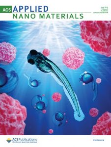
Cover of ACS Applied Nano Materials features the paper.

In research carried out in a number of Brazilian laboratories, a multidisciplinary scientific team developed a magnetic, luminescent nanomaterial capable of chemically binding to molecules of interest, such as drugs or proteins. This nanomaterial also showed low toxicity in tests with living organisms. With this set of characteristics, the new material can be seen as a multifunctional nanoplatform that is promising for the development of various applications, especially in the areas of biotechnology, health and environment. The study was reported in an article published in ACS Applied Nano Materials (American Chemical Society journal released in 2018), and featured on the cover of the June issue of the journal.

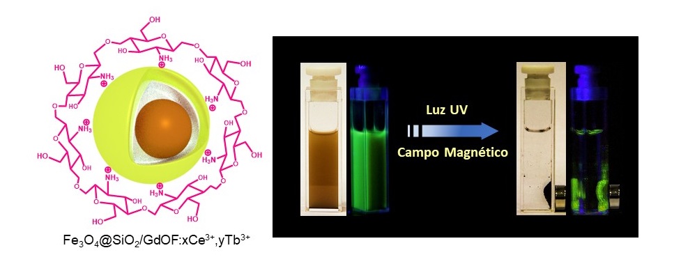
The properties of this nanoplatform derive from the presence of several compounds and elements with distinct properties: iron oxide (Fe3O4, known as magnetite) nanoparticles responsible for magnetism; lanthanide element ions (Gd3 +, Ce3 + and Tb3 +, known as rare earths) responsible for luminescence or light emission, and chitosan (biopolymer obtained from the crustacean exoskeleton), essential for providing chemical bonds of the nanoplatform surface to the external molecules of interest.

The nanoplatform was developed at the Brazilian National Nanotechnology Laboratory of the National Center for Energy and Materials Research (LNNano – CNPEM). The process used for its synthesis comprises a series of steps. Initially, the iron oxide nanoparticles that form the core of the nanoplatforms are synthesized and coated with silicon dioxide (SiO2). Then the luminescent elements and chitosan are incorporated into the nanoparticles forming an outer layer. The result is nanoplatforms of approximately 170 nm in diameter (on average), called Fe3O4@SiO2/GdOF:xCe3+,yTb3+.

On the left, a schematic illustration of one of the nanoplatforms, showing its core. On the right, a solution with nanoplatforms under the effect of a magnetic field (concentrated near the magnets) and irradiated with UV light (generating the emission of green light).

To study the magnetic and luminescent properties of the nanoplatform and to characterize its structure and morphology, research groups from the State University of Campinas (Unicamp) and the University of São Paulo (USP) participated in the study.

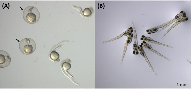
In addition, the main authors of the paper decided to evaluate the toxicity of nanoplatforms with relation to living organisms – a key step when thinking about health or environmental applications, and they decided to conduct a well-established in vivo test, in which zebrafish embryos (scientific name Danio rerio) are exposed to the material whose toxicity is to be evaluated. These freshwater fish, in fact, has a high genetic similarity to humans (about 70%) and at the same time is cheaper and easier to study than mice or rats, among other advantages.

In the toxicity test, a few dozen freshly fertilized zebrafish eggs were placed in aqueous medium containing the nanoplatforms at various concentrations. The embryos were examined at different development stages using an optical microscope to check for mortality, malformation, edema or changes in size. Tests included embryos with and without chorion (membrane that protects the embryo in the early stages of development). The test results carried out at LNNano showed that nanoplatforms, even at high concentrations (100 mg/L), have low toxicity for all embryo groups.

Zebrafish embryos used in nanotoxicity tests. (A) 24-hour embryos in the presence and absence of the chorion, where arrows indicate the chorion (membrane that protects embryos in the early stages of development). (B) Embryos after 96 hours of development.

“This work brings an unprecedented contribution that involves evaluating the toxicity of hybrid nanomaterials using the zebrafish model, a promising alternative method in nanotoxicology, and the influence of the chorion,” says Diego Stéfani Teodoro Martinez, CNPEM researcher at LNNano and one of the corresponding authors of the article.

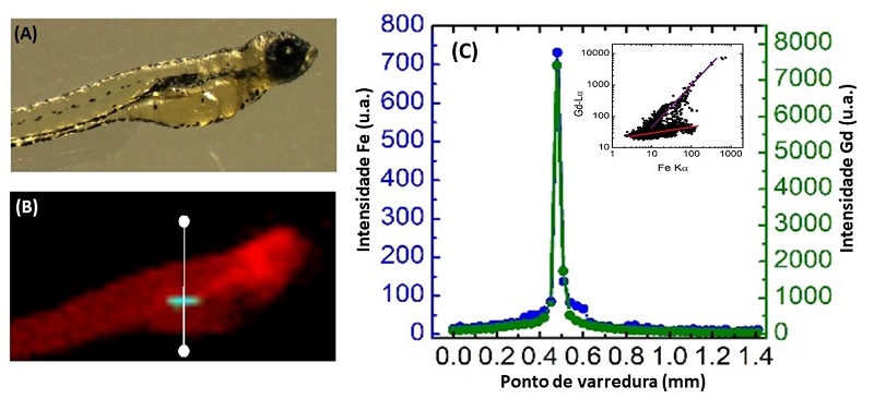
The embryos were also analyzed at the Brazilian National Synchrotron Light Laboratory (LNLS – CNPEM) to verify the distribution and concentration of nanoplatforms in the organism of the embryos. To do this, the scientists used the synchrotron light X-ray fluorescence microscopy (SXRF) technique, which can accurately map certain chemical elements in biological systems. This technique is available at one of the LNLS experimental stations, coordinated by the researcher Carlos Alberto Pérez, who is one of the corresponding authors of the article.

X-ray fluorescence microscopy analysis with synchrotron light (SXRF) of two zebrafish embryos after exposure to the nanoplatform for 72 hours. (A) Optical microscopy image of the embryos; (B) SXRF image of embryos demonstrating nanoplatform accumulation in the intestinal tract; and (C) X-ray fluorescence intensity along the white line indicated in (B), demonstrating the spatial co-location of Fe and Gd elements in the intestinal tract of zebrafish embryos.

SXRF analysis showed that nanoplatforms had accumulated in the embryos as a function of exposure time, with higher concentrations in the gastrointestinal tract in the case of already developed mouth embryos – a result that may be significant, for example in the context of healthcare applications involving oral nanoplatform ingestion.

The study was carried out in the context of a postdoctoral project by fellow Latif Ullah Khan, also corresponding author of the article. The completion of the project, says Martinez, was made possible by the availability of skills and facilities at CNPEM’s multi-user laboratories. However, partnerships with other laboratories were also crucial, adds the CNPEM researcher. Professor Marcelo Knobel’s group performed the magnetometry studies at Unicamp. The groups of professors Hermi Felinto Brito and Magnus Gidlund carried out the luminescence and functionalization studies at USP. Finally, Professor Diego Muraca (Unicamp) and researcher Jefferson Bettini (CNPEM) contributed to the structural and morphological characterization using transmission electron microscopy techniques.

“This article was the result of integrating the experience of different Brazilian groups; an interdisciplinary study on the frontier of knowledge in nanobiotechnology and nanotoxicology,” says Martinez, adding that one of the main challenges of the work was integrating knowledge and techniques from different areas, such as Materials, Biology and Toxicology, a task that was coordinated by Martinez and Pérez.

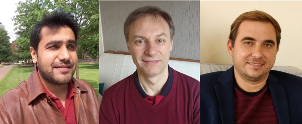
The main authors of the paper. From the left: Latif Khan, Carlos Pérez and Diego Stéfani Martinez.

The study received financial support from Brazilian agencies CAPES (including through the CAPES-CNPEM agreement), FAPESP and CNPq (including through INCT-Inomat); from the Brazilian Ministry of Science, Technology, Innovations and Communications (MCTIC) through SisNANO, and The World Academy of Sciences for advancement of science in developing countries (TWAS). The study also received financial support from the Brazil-China Nanotechnology Research and Innovation Center (CBC-Nano).

Applications: biotechnology, health and the environment

According to Martínez, the nanoplatform developed opens perspectives for applications in biotechnology, health and the environment, such as biological tissue and cell imaging systems, medical diagnostic kits, and environmental systems for pollutant detection and remediation

The applications would take advantage of the interesting set of nanoplatform properties. Because they are magnetic, using an external magnet, nanoplatforms could be directed and retained in a particular biological tissue or isolated from, for example, contaminated blood or water. In addition, the luminescence of the nanomaterial would allow visualizing the nanoplatforms within the biological tissues and cells of interest. Finally, the presence of chitosan would enable the chemical binding of drugs and other molecules that would serve for the diagnosis and/or treatment of diseases. “However, much study is still needed for real applications and commercialization of this nanoplatform, as it is a new material and needs to be tested on different models in the future,” says Martinez Martinez.


[Paper: Fe3O4@SiO2 Nanoparticles Concurrently Coated with Chitosan and GdOF:Ce3+,Tb3+ Luminophore for Bioimaging: Toxicity Evaluation in the Zebrafish Model. Latif U. Khan, Gabriela H. da Silva, Aline M. Z. de Medeiros, Zahid U. Khan, Magnus Gidlund, Hermi F. Brito, Oscar Moscoso-Londoño, Diego Muraca, Marcelo Knobel, Carlos A. Pérez, Diego Stéfani T. Martinez. ACS Appl. Nano Mater. 2019, 2,6, 3414-3425. https://doi.org/10.1021/acsanm.9b00339.]

Featured paper: Moving nanoparticles for asymmetric nanowires.

[Exploring Au Droplet Motion in Nanowire Growth: A Simple Route toward Asymmetric GaP Morphologies. Bruno C. da Silva*, Douglas S. Oliveira, Fernando Iikawa, Odilon D. D. Couto Jr., Jefferson Bettini, Luiz F. Zagonel, and Mônica A. Cotta*. Nano Lett., 2017, 17 (12), pp 7274–7282. DOI: 10.1021/acs.nanolett.7b02770]

Moving nanoparticles for asymmetric nanowires.

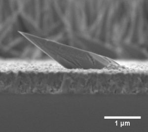
Scanning electron microscopy image of asymmetric gallium phosphide (GaP) nanowires.

A team of scientists presented a route to grow semiconductor nanowires having an asymmetric morphology, different from the traditional cylindrical one. The possibility of producing, in a controlled manner, nanowires with particular formats and without defects, can be exploited in several applications, including the production of more efficient solar cells.

The research was led by scientists from the Brazilian university UNICAMP and the Brazilian Nanotechnology National Laboratory (LNNANO), who reported their findings in a paper in NanoLetters.

The researchers discovered the process while studying the production of nanowires of gallium phosphide (GaP) for optoelectronic applications. The team chose to produce the nanowires by chemical beam epitaxy (CBE), preceded by a thermal treatment (annealing). In this technique, a substrate of a suitable material – in this case gallium arsenide (GaAs) – is placed inside a chamber. Then, chemical compounds in the form of vapor are introduced into the chamber. Some elements of the vapored material deposit over the substrate, layer upon layer, generating films. To promote the growth of nanowires instead of films, metallic nanoparticles (in this case, gold nanoparticles) are placed on the substrate before being exposed to vapor. During exposure, these catalytic nanoparticles cause the material to deposit preferentially underneath them, causing wire-like structures to grow.

While the researchers were analyzing the nanowires they had obtained in the first few months of the work, they found a significant amount of asymmetric nanostructures. “Besides having a particular morphology, we saw that these nanowires had an hexagonal crystal structure (wurtzite) and a very low density of crystallographic defects, which motivated us to study in detail the causes for the formation of this unusual structure,” says Bruno da Silva, PhD student at UNICAMP and corresponding author of the paper.

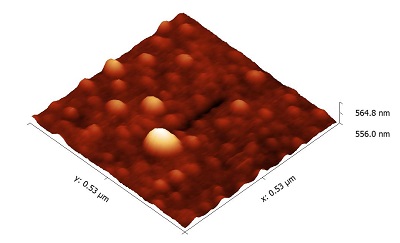
Da Silva and his supervisor Prof. Mônica Cotta then began to raise and test hypotheses for the cause behind the formation of the peculiar structures. After several experiments and analyses, they focused on a phenomenon that caught their attention: in the early stages of the process, the gold nanoparticles spontaneously moved over the substrate. Hence, the duo undertook a systematic work on heating substrates with nanoparticle catalysts, growing nanowires under various conditions, and analyzing the resulting samples through scanning and transmission electron microscopes and atomic force microscopy.

Atomic force microscopy image of a gold nanoparticle on GaAs substrate showing the trail left by its movement.

Da Silva, Prof. Cotta and their collaborators from UNICAMP and LNNano were able to find out why the growth process they used resulted in asymmetric nanowires. The main reason was the movement of the gold nanoparticles, which was thermally activated with the initial annealing. Based on that discovery, the team established a recipe for producing asymmetric semiconductor nanowires in a controlled manner. “Our work was the first to show that the mechanical instability of the nanoparticle catalyst can be used to modify the growth of semiconductor nanowires, in our case, particularly affecting their morphology,” says Bruno da Silva.

The mechanism of the asymmetric nanowires growth presented in the NanoLetters paper can be described as follow. When heated together with the substrate, the nanoparticles begin to crawl and advance through the substrate while consuming the oxide layer that naturally covers the gallium arsenide. Thus, the nanoparticles form asymmetric grooves a few nanometers deep and a few hundred nanometers long. These trails become fertile ground for the growth of the nanowires, since the deposition rate of the vapored material is greater there than in the rest of the substrate, which is covered by the oxide. A pedestal then forms along the grooves and the nanowire grows on top of the pedestal with an asymmetrical format.  “We showed that the movement of the particle generates a zone of preferential deposition, and that the combination of this phenomenon with the axial growth “vapor – liquid – solid” leads to the asymmetry in the nanowire,” summarizes da Silva.

Besides describing the formation mechanism of asymmetric nanowires, the work of the Brazilian team generated detailed knowledge about the movement of heated metallic nanoparticles. “We have shown that in addition to temperature, vacuum conditions and surface quality of the substrate are crucial for nanoparticle stability, and that the motion direction is related to the asymmetry of gold dissolution on semiconductor surfaces III-V,” details the doctorate student.

Concerning possible applications, the asymmetry of these nanowires can be explored, for example, in the construction of antireflective layers that reduce the amount of light lost by reflection in solar cells.  Another possibility would be to exploit the green emission of these wurtzite gallium phosphide nanowire in lighting devices. Or, why not, to develop an alternative process to electronic litography taking advantage of the gold nanoparticles movement and the trails it forms on the substrate.

The work was funded by Unicamp, the Brazilian federal agencies CNPq and CAPES and the São Paulo Research Foundation (FAPESP).


People from our community: interview with Adalberto Fazzio.

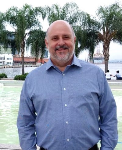
Prof. Adalberto Fazzio

Since April of this year, the Brazilian Nanotechnology National Laboratory (LNNano) of the National Center for Research in Energy and Materials (CNPEM) is headed by the scientist Adalberto Fazzio, 66, born in the São Paulo state city of Sorocaba.

Adalberto Fazzio has been studying materials through computational tools for over four decades. He pioneered in Brazil the use of ab initio calculations, widely used in the study of materials properties, and made significant contributions toward understanding transition metals, amorphous systems, gold (Au) and silver (Ag) thin films, carbon nanostructures, silicon, topological insulators, and other materials. Fazzio and his research group, known as SAMPA (acronym for “Simulations Applied to Atomic Materials and Properties”), have successfully worked on this at the Institute of Physics of the University of São Paulo (USP) and also with several theoretical and experimental collaborators from Brazil and abroad.

Adalberto Fazzio received his undergraduate (1972) and master’s degree (1975) in Physics at the University of Brasília (UnB) and his doctorate (1978),also in Physics, at USP.

Fazzio became a professor at the Institute of Physics – USP in 1979, shortly after completing his doctorate. In 1985 he became an associate professor at that university and in 1991 he became full professor. He was a visiting researcher at the National Renewable Energy Laboratory (USA) from 1983 to 1984 and at the Fritz-Haber-Institut der Max-Planck-Gesellschaft (Germany) from 1989 to 1990. In May 2015, he retired from USP. He was a visiting Professor at the Brazilian Federal University of ABC (UFABC) in 2016.

Throughout his career, Fazzio has held several management positions, such as president of the Brazilian Society of Physics (SBF) from 2003 to 2007; pro tempore president of UFABC from 2008 to 2010; micro and nanotechnologies general coordinator at the Ministry of Science, Technology and Innovation (MCTI) in 2011; assistant secretary of the Technology, Development and Innovation Secretariat of MCTI from 2011 to 2013, and director of the Institute of Physics – USP from 2014 to 2015.

He has also received other honors, such as the Brazilian National Order of Scientific Merit in 2006 (promoted to the Grand-Cross class in 2010). In 2013 he was elected a fellow of TWAS (The World Academy of Sciences). He is a member of several scientific societies, such as the Brazilian Academy of Sciences and the Academy of Sciences of the State of São Paulo in Brazil, and the American Physical Society, American Chemical Society and Materials Research Society in the United States.

Fazzio is the author of over 270 articles published in indexed scientific journals. His scientific production has about 8,000 citations, according to Google Scholar. He has supervised approximately 40 master’s and doctoral students.

Here is an interview with the scientist.

SBPMat Bulletin:  Tell us what led you to become a scientist and in particular to work in the area of Condensed Matter Physics.

Adalberto Fazzio:  When I finished my Physics course at the University of Brasilia in 1972, I met Professor José David Mangueira Vianna, who had returned from Switzerland with many projects on Molecular Physics. At that time we were talking about quantum chemistry. He presented a master’s project that was an improvement on semi-empirical models based on the Hartree-Fock method. Due to the low computational capacity of that time, these methods originating from the ZDO (Zero Differential Overlap) approximation were the most widely used to shed light on the electronic properties of molecules. After my master’s degree, I went to the Institute of Physics – USP in the group of Professors Guimarães Ferreira and José Roberto Leite (my doctoral advisor), changing from molecules to solids and from Hartree-Fock to DFT (Density Functional Theory). At that moment I became a Condensed Matter Physicist in a Department of Physics of Materials created by Professor Mário Schemberg. My thesis was about deep level impurities in semiconductors. Bear in mind this was in 1976 and the question was how to treat a crystal that has lost its translational symmetry. Finally, I developed a model, “Molecular Cluster Model for Impurities in Covalent Semiconductors.”

SBPMat Bulletin:  What do you believe are your main contributions to the Materials area? We would like to ask you to go beyond listing the results and to briefly describe the contributions you consider as the most relevant. In your response, we ask that you consider all aspects of scientific activity. Feel free to share references to articles and books, if relevant.

Adalberto Fazzio: Whenever we reflect on the main contributions in a given area, we look at the most cited articles, which do not always correspond to the articles that the authors would expect to be the most cited. But I will try to give you a brief description of some of the themes in which I believe I made a contribution that was highlighted. In the study of defects and impurities in semiconductors, I highlight the study of transition metals (TM) in semiconductors. At the time – until 1984 – there was a wealth of experimental data concerning the position of levels of impurities in the gap and the optical excitations of all MT-3ds. And the theoretical calculations based on a medium-field theory did not explain these data. During my post doctoral research at NREL (National Renewable Energy Laboratory) in 1983/84, we developed a model to describe the experimental data. It was a model that coupled the field crystal theory with the DFT theory, which described effects of multiplets from the TM impurities. Several articles were published applying this model. The model is presented in detail in Phys. Rev. B 30, 3430 (84). This work was in collaboration with the researchers Alex Zunger and Marilia Caldas. And those results led to a letter in the Appl. Phys. Lett. (1984) which would be of great interest to experimental physicists, titled “A Universal trend in the binding energies of deep impurities in semiconductors”. A major change occurred in this area in the late 1980s, with the “Large Unit Cell” calculations, DFT method and pseudo potentials. Today known simply as “ab initio methods” or “free parameters”. Regarding this development, I was at the Max Planck Institute in Berlin, working with Matthias Scheffler. Together with my doctoral students (T. Schmidt and P. Venezuela), we were pioneers in the use of this type of methodology in Brazil, widely used until now. After these studies, I started working with amorphous systems. Since we could now work with systems containing many atoms per unit cell, we decided to couple the ab initio calculations using structures generated by Monte Carlo simulations. I highlight two papers: one in a-SiN (PRB, 58, 8323 (1998)) and a-Ge:N (PRL 77, 546 (96)).

At the end of the 1990s, at the Brazilian National Synchrotron Light Laboratory (LNLS),  Professor Daniel Ugarte was performing beautiful experiments with HTEM, where he observed the formation of linear chains of atoms in Au and Ag fine films. Our group at USP, in cooperation with Edison Zacarias at UNICAMP, had begun studies to understand the formation of linear chains of Au atoms. Some of the questions were about how these chains broke and how we could explain the great distances that appeared between atoms. This experiment-theory interaction was a very important moment. Several papers were published, one which was widely cited “How do gold nanowire break?” (PRL 87, 196803 (2001)). This work was the cover of PRL and highlighted by the editor of Science. And later we showed how oxygen acts to trap the Au atoms in the wires (PRL 96, 01604 (2006)) and the effects of temperature and quantum effects on wire breakage and stability, important aspects to understand the observations (PRL 100, 0561049 (2008)).

In the same period, our group at USP focused on the study of nanostructures of carbon, silicon, etc. Although we had strong tools for describing electronic, magnetic, optical and mechanical properties, the understanding of these materials lacked the properties of electronic transport. In this context, we developed a computational code based on the Landauer-Büttiker theory. Several PhD students were involved in this code, which is known as TRANSAMPA.  And, in my opinion, several important works were carried out to better understand the behavior of electronic transport properties. To exemplify this, we were pioneers in describing the transport in doped graphene tapes (PRL 98,196803 (2007)). I should also mention the collaboration with Professor Alexandre Reilly from IFT (Institute of Theoretical Physics of UNESP) who was then a post-doc, which resulted in a very important improvement of this code, and which allowed to treat materials with the realistic dimensions used in the experiments. In 2008, in a paper titled “Designing Real Nanotube-based Gas Sensor” (PRL 100, 176803), we showed how nanotubes can function as realistic-sized sensors, with defects. Using first-principle calculations, we had systems of micrometric dimensions within our reach.

Currently, my research is more focused on the search for devices formed by 2D materials whose interface is primarily built by van der Waals interactions. For example, like graphene, a new 2D material was isolated from exfoliated black phosphorus, also called phosphorene. We studied the graphene/phosphorene interface (PRL 114, 066803(20015)), showing how a device can be constructed.

Another class of materials I have been working on concerns the well-known topological insulators. A Topological Insulator (TI) is a material that has no states of energy gap “at the edges” and whose “bulk” is insulating! These states are topologically protected and robust against disturbances. In the case of two-dimensional (2D) materials (2D), they are known as insulators that feature Quantum Spin Hall (QSH). The scattering surface state is protected by time reversal (TR) symmetry, leading to an electronic transport without energy dissipation. In 2011, together with the UFU group, we showed how magnetic impurities in topological insulators have their spin texture modified (PRB 84, 245418 (2011)). Recently, in collaboration with Professor Zhang from the Rensseler Polytecnic Institute, we presented a general model for describing the topological/trivial interface. We showed, for example, the Bi2Se3/GaAs interface. There were replicas of the Dirac cone that emerged from the interface interaction including semiconductor states (Nature Comm. 6, 7630(2015)). Phosphorene is a 2D material that has semiconducting properties. In cooperation with the group of Professot Alez Zunger, of the University of Colorado, we studied this material under the action of an electric field and showed that for three or four layers of phosphorene, under the action of the field, it has a topological transition (NanoLett. 15, 1222 (2015)).

Finally, I would like to mention an activity that I am initiating, which is the use of Machine-Learning techniques for material properties. In particular, I have focused on topological insulators. And as I mentioned earlier, specifying the more relevant studies I have left out many others.

As for other types of contributions, together with José Roque I built a very productive group at IF-USP, known as SAMPA (Simulation Applied to Materials – Atomic Properties) where numerous doctors and masters, and several postdocs were cultivated. I should add that all this was possible mainly due to the support of Fapesp, via thematic projects. I was head of the Department of Materials Physics, Director of IFUSP and pro tempore Director of the Federal University of ABC. From a management point of view, I would like to highlight my participation at the Ministry of Science, Technology and Innovation, where I was the Under-Secretary of Setec (Technology and Innovation Secretariat) and SCUP (Secretariat of Research Units). And I am proud to have coordinated the creation of the Brazilian Nanotechnology Initiative, where the SISNANO system is an important arm – a set of laboratories dedicated to technological research and development.

I also wrote two books that have been adopted: “Introduction to Group Theory: applied in molecules and solids”, together with Kazunori Watari and “Quantum Theory of Molecules and Solids”, together with José David Vianna and Sylvio Canuto.

SBPMat Bulletin:  You have just taken on the direction of the Brazilian National Nanotechnology Laboratory (LNNano). Please share with the Materials community your plans for LNNano. How do you see the situation of nanoscience and nanotechnology research in Brazil given the recent budget cuts?

Adalberto Fazzio:  Two weeks ago I took on the direction of the National Nanotechnology Laboratory (LNNano), one of the four National Laboratories of the National Center for Research in Energy and Materials (CNPEM). This is a laboratory recognized for its excellence, dedicated to the production of knowledge in nanotechnology, moving from basic science to technological innovation.

I was very happy and I hope to continue the work of the researchers who were at the forefront of LNNano and who preceded me, such as Daniel Ugarte, Fernando Galembeck and Marcelo Knobel. This is the laboratory that holds a management bond with MCTIC fully dedicated to nanotechnology.  One of its main missions is to service external users through open equipment. An example is the electron microscopy and probes park, which is certainly the best equipped in Latin America.  LNNano is the main executor of government policies in the area. We have intense in-house mission-oriented research activity with impact studies. We are currently undertaking minor restructurings to better serve external users and to strengthen ongoing research.

The nanotechnology platform has raised considerable resources in all developed countries of the world. For example, the US government has annually deposited something in the order of US$ 1.8 Bi. Unfortunately, in Brazil we have had difficulties to provide continuity to even much more modest programs. However, the community has responded with great capability to the development of nanotechnology products. Today, for example, anchored in the SISNANO system, we have about 200 companies seeking innovation in the Nano area; and in particular, the performance of LNNano has been outstanding.

What we cannot however, is face budget cuts in science and technology every year. We are in a very delicate moment in our economy, low growth, but it is imperative to preserve the achievements of the last decades in the area of science and technology. The programs in the area of research and technology development must be preserved. This is because when the crisis is over, the country must be prepared to continue growing. Therefore, it is fundamental to continue generating new knowledge, striving for technological innovation and also training qualified human resources. In other words, the economic slowdown should not be accompanied by investment cuts in technology and development research.

SBPMat Bulletin:  Please leave a message for the readers who are starting their scientific careers.

Adalberto Fazzio:  The greatest wealth in our country is human capital. Brazil has a large young population, young people who are often in the middle of the path in their scientific and technological careers, because they are not able to envision in the future the acknowledgment and respect for a fundamental activity, which is the search for knowledge. Those who desire to pursue a scientific career must persevere and stand firm in their studies.