Featured scientist: Edson Roberto Leite.

Prof Edson Roberto Leite

Edson Roberto Leite memories related to science are all very pleasant: the book about rockets in his childhood in the interior of São Paulo, the opportunity to use an exceptional microscope during the sabbatical period in the United States, the discovery of a mechanism for the growth of nanocrystals at the Brazilian National Synchrotron Light Laboratory…

Some of these wonderful memories include the many occasions experienced alongside his tutor and scientific father, Professor José Arana Varela, a prominent Brazilian materials scientist who died in 2016. Arana Varela was honored by B-MRS with the creation, in 2019, of an award that bears his name, and which annually distinguishes a prominent researcher from Brazil, who gives a plenary lecture at the Society’s annual event. In its first edition, the award was befittingly granted to Edson Roberto Leite, professor at the Federal University of São Carlos (UFSCar) and scientific director of the Brazilian National Nanotechnology Laboratory (LNNano-CNPEM). Leite is also editor for Latin America of the Journal of Nanoparticle Research (Springer).

Edson Roberto Leite received his first degree in Materials Engineering from UFSCar in 1988. In doubt between pursuing a career in industry or academia, he initially tried to reconcile both. After graduating, he worked in the research and development area at 3M, while doing his master’s degree and starting his doctorate, both in Materials Science and Engineering at UFSCar. In 1992, he left the company in order to dedicate his time to the doctorate, a decision that he recalls did not please his father-in-law, who was concerned with the livelihood of the family that by now included two children. However, over the years, the results of this decision have been very positive. In 1994, shortly after defending his doctorate, Leite became a professor in the Chemistry Department at UFSCar and started a career as a researcher in materials, which would not only be fruitful, but also enjoyable.

Co-author of more than 400 scientific articles published with more than 19 thousand citations, today Leite has an h index of 72 (Google Scholar). The scientist is also the editor of three books related to materials for energy and co-author of a book on the process of nucleation and growth of nanocrystals. Leite received several awards, including the Scopus Prize from Elsevier/CAPES (2006), for the excellence of his scientific production as a whole, and the John Simon Guggenheim Memorial Foundation Fellowship (2009), awarded to scientists with exceptional research skills. In 2012, Edson Leite was elected member of the World Academy of Ceramics and the Academy of Sciences of the State of São Paulo. In 2014, he was cochair of the Spring Meeting of Materials Research Society, held in San Frascisco (USA). In 2019 he was elected full member of the Brazilian Academy of Sciences (ABC).

Read our interview and learn more about this scientist, his main contributions and his memories of Professor Arana Varela.

B-MRS newsletter: At school, you had more affinity with science subjects, right? Do you remember how this taste for science originated?

Edson Roberto Leite: A person’s story always has the personal version and the version of the people who interacted with him. I will recount my perspective of how it happened.

At school I always had a strong affinity for Science and History. A striking memory was when I was in the third grade of elementary school and my father took me to the Municipal Library of Araras to take out a membership card so I could access books. The first book I chose was about rockets. I have always loved the conquest of space and the science behind fundamental historical moments. It is noteworthy that man had reached the moon only a few years earlier, nuclear power was seen as the global energy solution and semiconductors were just beginning.

In addition to this fond memory, there were other motivations, including Jonny Quest, a really cool cartoon. This animation, in addition to the adventures, had a lot of science fiction, and Jonny’s father (Dr. Benton Quest) was a renowned scientist with an excellent research laboratory in his own home.

My childhood, then, was always marked by a strong influence of science classes. I think it easily guided me to choose Engineering. At first the idea was to become a mechanical engineer, but during my prep course for the entrance exam I was introduced to Materials Engineering, at UFSCar. I took the exam in the middle of 1983 and passed. From then on I knew what I wanted and what I liked.

However, there was still a doubt, whether to go to the academic area or go to industry (my father was a Nestlé employee in Araras and the industrial sector always caught my attention). During my undergraduate studies, I went to live at the student housing headed by Celso V. Santilli (today an important researcher in the field of Materials, Professor at IQ-UNESP-Araraquara) and he helped me to participate in an undergraduate research program with professors Elson Longo and José Arana Varela. That was when I learned what science was and that increased my taste for the academic area. In 1984, I had the first undergraduate scholarship from FAPESP under the guidance of Professor Varela (who was a visiting professor in the Materials Engineering department (DEMa) at UFSCar). In 1988 I graduated, joined the DEMa-UFSCar master’s degree program and went to work as a development engineer at 3M do Brasil, in Sumaré, SP. My director at 3M was the engineer Aloysio Pizarro and he released me for the master’s degree (which I defended in 1990 under the guidance of Professor Elson) and for the doctorate (in 1990). In 1992, I realized it would be impossible to reconcile the research area and my activities at 3M, so I left 3M to focus entirely on my academic research, returning to São Carlos. I finished my doctorate in 1993 under the supervision of Professor José A. Varela. In January 1994, I became an adjunct professor in the Chemistry department at UFSCar and joined LIEC (Interdisciplinary Laboratory of Electrochemistry and Ceramics), founded by Elson, Varela and Bulhões (Professor Luís Otávio S. Bulhões). I went back to the place that had introduced me to science.

Those moments influenced me…

B-MRS newsletter: In your assessment, what are your main contributions to the Materials area?

Edson Roberto Leite: Ever since undergraduate research, I have been working mainly with inorganic materials, more specifically with ceramic materials. So, I will report the contributions I believe are most important, according to my point of view (in fact these may be the contributions I most enjoyed working with).

Since 1994 I have been working with chemical and physical-chemical materials and have been involved in several areas, among them: chemical synthesis of ceramic oxides, synthesis of nanoparticles with controlled size and morphology, growth of nanocrystals, electrical properties of ceramic oxides, materials for application in alternative energy devices and transmission electron microscopy (TEM). During this period, always developing works in collaboration with professors Elson Longo and José A. Varela, at LIEC of DQ-UFSCar. Among these different areas I will highlight my contributions to the growth of nanocrystals and the work on alternative energy.

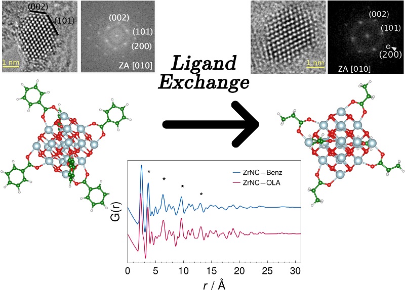
In 1998, that is, 4 years after I was hired, I went on a sabbatical in the USA, in the group of Professor Martin P. Harmer, at Lehigh University (Betlehem, PA). In my sabbatical, I worked on converting polycrystalline ceramics into monocrystalline ceramics, using controlled grain growth. It was a wonderful year and my recollection of that period is vivid in my memory. I still remember the smell of the laboratory and the friendships I cultivated. From a professional point of view, the work drew my attention to the process of solid-state crystal growth. My contribution to the project was to characterize the growth process using advanced transmission electron microscopy techniques. At that time I had the opportunity to operate the VG-603 analytical transmission electron microscope. There were few microscopes like this being produced, and I still remember the words of the coordinator of the Lehigh microscopy laboratory, Dr. Dave Ackland saying that “few researchers in the world have had the honor of operating this equipment.” Returning to Brazil in 1999, I dedicated a lot of my time to microscopy and, with the help of the newly created Electronic Microscopy Laboratory of LNLS (created in 1997 by Dr. Daniel Ugarte), I began studying the process of growing nanocrystals in colloidal solution. I quickly identified, for SnO2 nanocrystals, a growth mechanism recently described in the literature known as “Oriented Attachment” (OA). The first article we published about this nanocrystal growth mechanism was in 2003. During this period I created a group of high-level master and doctoral students (today these students are researchers and professors), which truly allowed exploring this growth mechanism. In fact, we published, almost simultaneously with American groups, the first kinetic model to describe this growth process, and shortly afterwards we published two important articles, one related to the growth of anisotropic nanocrystals and the other correlating the OA process with a polymerization process. Both articles are considered pioneers in the area. International recognition in the area came with the invitation to publish two review articles (one at Nanoscale and the other at CrysEngComm), one of them in collaboration with leading international experts in the field of nanocrystal growth kinetics by OA.

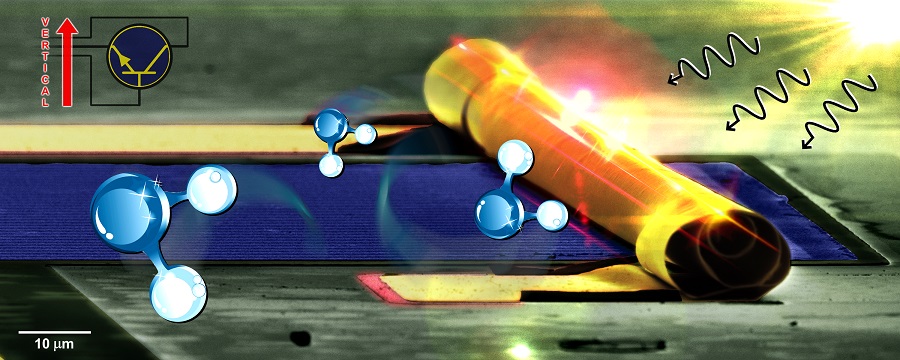
I started working in alternative energy in 2004, when I helped organize a symposium on the theme at the MRS Spring Meeting in San Francisco. After that, we invested in this area and, with a new group of brilliant students, we achieved fantastic results, between 2007 and 2016, regarding the development of hematite photo anodes to promote water photo-electrolysis aimed at hydrogen production. We developed an electrode manufacturing process based on colloidal nanocrystal deposition. This enabled the highest impact publications of my career, in journals such as JACS and Energy Environ. Sci. In the same period we developed a method for synthesizing MoS2 (2D material), combining non-hydrolytic sol-gel method and microwave reaction. This again resulted in excellent materials for electrocatalysis and for supercapacitors. This research also enabled publications in high-impact journals, such as Chem. Comm and Advanced Energy Materials. Without a doubt, this team of students placed us in the state-of-the-art to develop materials for alternative energy.

I would like to highlight just one more important contribution, which was in the study of the combustion process in glass-melting furnaces, carried out with funding from White Martins/Praxair. In this work, carried out with Professor Carlos Paskocimas (currently at UFRN) and Professors Elson and Varela, we characterized the corrosion rate of the furnaces and proposed technological solutions to inhibit this corrosion. This work was a success at the time and we were invited to present the results at Corning Glass and Praxair in the United States.

B-MRS newsletter: You were celebrated in the first edition of the B-MRS José Arana Varela award, which honors this prominent Brazilian scientist (who died in 2016), former president of B-MRS. Professor Varela was your doctoral advisor and co-author of many published articles. Could you share with us some memories about Professor Varela and comment on the scientific partnership both of you developed over time? Feel free to leave any more personal comments.

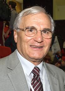
Edson Roberto Leite: As I mentioned above, I was introduced to Professors Varela and Elson during my undergraduate years, and Professor Varela was my undergraduate and PhD advisor. In fact, I was Varela’s first doctoral student, in 1993. Being the first to win this award is an honor, which made me very happy. Besides being my advisor, Professor Varela was a tutor and almost a father, teaching me and introducing me to the national and international scientific community. It was with him that I made my first trip abroad, in 1993, where he introduced me to the great names of international Ceramics at the American Congress of The American Ceramic Society. It was at this opportunity that I met Professor Gary Messing and Professor Harmer. I remember him introducing me to the famous Professor W.D. Kingery, the father of modern Ceramics. It was Varela who encouraged me to be a member of World Academy of Ceramics. There were several trips, opening new work fronts and new research areas. As a tutor and advisor he knew how to get my attention and point out my mistakes. I remember, more recently, at an MRS Fall meeting in Boston (USA), a long discussion that we had where he, without hesitation, “pulled my ear” and helped me handle future problems I would face as a group leader in the Materials Chemistry area. I know he saw me as a rebellious student, but I’m sure he was proud of the training he gave me. His premature death took me by surprise and I miss him very much. I miss our discussions, our conversations and especially his advice and guidance.

B-MRS newsletter: Please leave a message for our younger readers who are starting a scientific career or are evaluating this possibility.

Edson Roberto Leite: I am not good with words, my students and former students know that I am very direct. I never worried about planning my career, everything was happening as I followed my instincts. What I am today is largely due to my students and the support of two scientific parents, professors Elson and Varela. My job is not a job, it is a hobby. So my message is: To achieve success in a scientific career you must really like what you do.

B-MRS Newsletter. Year 7, issue 2.


logo header 400

Newsletter of the
Brazilian Materials
Research Society

Year 7, issue 2. March 11, 2020.

B-MRS News

New B-MRS board. Get to know the members of the new executive board: their academic training, research topics, what they like to do when they are not working and more. See here.

– Swearing-in ceremony. B-MRS new executive board, chaired by Professor Mônica A. Cotta, took office at a ceremony held at IFGW-Unicamp on the morning of February 14, attended by more than 80 people, including authorities from the Brazilian Ministry of Science and Technology, scientific societies, research centers and universities. In their brief speeches recurrent subjects were women in science and the social impact of research. Know more.

– Note in defense of democracy. B-MRS and dozens of Brazilian scientific entities endorsed SBPC’s note in defense of democracy, published on February 26. Know more.

Featured Paper

A research group from the Brazilian Nanotechnology National Laboratory developed a memristor and a transistor with hybrid materials (organic – inorganic) and microtubes made of self-rolled nanomembrane. The new components can contribute to the development of smaller, flexible and cheaper devices that combine better performance and lower energy consumption. The works were recently reported in Nano Letters and Nature Communications. Know more.

paper_news

From Idea to Product

We tell the interesting story of Kevlar, a lightweight and super resistant material used in hundreds of products from dozens of different markets. The story begins with a fundamental science discovery made by a woman without a PhD, who found in the laboratories of the DuPont company, in the middle of the last century, a favorable environment to develop her talent and passion for scientific research. Know more.

stephanie news

News from B-MRS Members

– Prof. Victor Carlos Pandolfelli (DEMa-UFSCar), B-MRS member, received an award from TMS (The Minerals, Metals and Materials Society, USA) for papers that show the application of science in solving practical problems. Know more.

19 encontro_banner_560 px

XIX B-MRS Meeting + IUMRS ICEM 2020
(Foz do Iguaçu, Brazil, August 30 – September 3, 2020)

Website: www.sbpmat.org.br/19encontro/

Abstract submission is open by April 1st!

Abstract submission. Deadline: April 1st. Guidelines for preparing and submiting abstracts, here. Guidelines for oral and poster presentations, here.

Symposia. The event comprises 29 thematic symposia. See the list, here.

Registration. The registration system is open. July 15 is the deadline for early registration (with discount). The fees include three lunches, besides the coffee breaks and the welcome cocktail. Know more, here.

Exhibitors and sponsors. 15 companies have already confirmed their participation as exhibitors-sponsors of the event. Companies and other organizations interested in participating in the event as exhibitors, sponsors or supporters, can contact Alexandre at comercial@sbpmat.org.br before March 31.

Student awards. Authors of works that are undergraduate, master’s or doctoral students may compete for the B-MRS and ACS Publications awards by submitting extended abstracts after receiving notification of acceptance of their conventional abstracts. More information in the instructions for authors, here.

International plenary lectures. Renowned scientists from China, Italy, Japan and USA have already confirmed their presence as speakers at the event. Know more at the event website.

José Arana Varela Lecture (national plenary lecture). Professor Edson Roberto Leite (LNNano – CNPEM) was chosen by B-MRS to receive this distinction and will give the lecture at the event.

Joaquim da Costa Ribeiro Memorial Lecture. The honor goes to Professor Cid Bartolomeu de Araújo (UFPE), who will give the lecture at the event.

Venue. The event will be held at Rafain Palace Hotel and Conventions, located in Foz do Iguaçu (Brazil). Know more.

Accommodations. See accommodation options from the event official travel agency, here.

Joint event. The event brings together the 19th edition of the B-MRS annual meeting and the 17th edition of the International Conference on Electronic Materials organized every two years by the International Union of Materials Research Societies (IUMRS).

Organization. Professor Gustavo Martini Dalpian (UFABC) is the general coordinator, Carlos Cesar Bof Bufon (LNNano) is the program coordinator and Flavio Leandro de Souza (UFABC) is the general secretary. At the international committee, the event features scientists from America, Asia, Europe and Oceania. Know more at the event website.

Reading Tips

– Scientists increase the efficiency of converting CO2 into methanol by developing and using an intelligent membrane, whose nanochannels drain water, but prevent the passage of gases. This membrane can accelerate several industrial processes limited by the presence of water (Science). Know more.

– Brazilian advances in perovskite synthesis and characterization: scientists are able to produce new 2D perovskite and also individually map nanometric grains of perovskite films, opening possibilities for the application of these materials in LEDs and solar cells (Chemistry of Materials and Science Advances). Know more.

Events

Pan American Ceramics Congress and Ferroelectrics Meeting of Americas (PACC-FMAs 2020). Panamá (Panamá). July 19 – 23, 2020. Site.

International Conference on Science and Technology of Synthetic Materials (ICSM 2020). Glasgow (UK). July 26 – 31, 2020. Site.

XVIII International Congress on Rheology. Rio de Janeiro, RJ (Brazil). August 2 – 7, 2020. Site.

XIX B-MRS Meeting + 2020 IUMRS ICEM (International Conference on Electronic Materials). Foz do Iguaçu, PR (Brazil). August 30 – September 3, 2020. Site.

XLI Congresso Brasileiro de Aplicações de Vácuo na Indústria e na Ciência. Foz do Iguaçu, PR (Brazil). October 5 – 7, 2020. Site.

5th International Conference of Surfaces, Coatings and NanoStructured Materials – Americas (NANOSMAT-Americas). Foz do Iguaçu, PR (Brazil). October 7 – 10, 2020. Site.

7th Meeting on Self Assembly Structures in Solution and at Interfaces (AutoOrg). Bento Gonçalves, RS (Brazil). November 4 – 6, 2020. Site.

Follow us on social media

You can suggest news, opportunities, events or reading tips in the materials field to be covered by B-MRS Newsletter. Write to comunicacao@sbpmat.org.br.


Featured paper: Nanomembrane microtubes and hybrid materials for advanced electronic devices.

Some of the challenges of the next generation of smartphones, sensors and other electronic devices can be solved with the help of nanomembrane microtubes (sheets made from various materials with nanometric thicknesses and micrometric lateral dimensions, which can be self-rolled and form microtubes).

In the city of Campinas (São Paulo State), at the Brazilian Nanotechnology National Laboratory of the National Center for Research in Energy and Materials (LNNano / CNPEM), a group of scientists has developed expertise in processes for the synthesis, manufacture and characterization of nanomembranes and their applications. In papers published in January and February of this year in the journals Nano Letters and Nature Communications, the authors explore some nanomembrane potentials, mainly related to their flexibility and dimensions, to develop new memristors and transistors – two widely used electronic devices.

More precisely, the LNNano researchers show that nanomembrane microtubes can be key parts in the manufacture of promising components using organic and hybrid materials (organic-inorganic) such as memristors and transistors. Thus, the novelties proposed in the articles can contribute to the development of even smaller, flexible, portable, cheaper devices and equipment that combine better performance and more low energy consumption features.

In an interview with the B-MRS Newsletter, Carlos Cesar Bof Bufon, corresponding author of both articles, talks about the scientific, technological and social impact of the research and about the skills and infrastructure involved in carrying it out. Bufon is a researcher and head of the Devices Division at LNNano/CNPEM.

B-MRS Newsletter: The articles present advances, developed at LNNano, in technologies for electronic devices (transistors and memristors). In your opinion, what are the main technological and/or scientific contributions of these articles?

Carlos Cesar Bof Bufon: The work entitled “Ambipolar Resistive Switching in an Ultrathin Surface-Supported Metal–Organic Framework Vertical Heterojunction” published in Nano Letters (DOI: 10.1021/acs.nanolett.9b04355), reports the development of a new type of memristor using structures called Surface-Supported Metal-Organic Frameworks (SURMOFs). SURMOFs are hybrid structures composed of metallic ions connected by organic ligands. The structure is highly organized on surfaces covered with chemically active self-assembled monolayers (SAMs). There are more than 70 thousand types of metal-organic structures (MOFs) that can be prepared as SURMOFs to confer new features to electronic devices. In addition to the unique properties, its considerable mechanical flexibility and low cost arouse interest in the scientific community for applications. However, in the case of a hybrid material consisting of organic and inorganic elements, the integration of this class of nanomaterials becomes a technological challenge. To circumvent this limitation, this work presents a new architecture for the integration of these SURMOFs structures for the development of a new type of memristor. The proposed architecture is based on the upper electrical contact of SURMOF HKUST-1 ultrathin films using self-rolled metal nanomembranes (microtubes). The SURMOF films explored in this work have thicknesses of the order of 20 nanometers. This new architecture opens up promising paths in the area of electronic devices based on SURMOFs, as well as providing a technological platform for conducting studies not yet reported in the literature for this class of materials. For example, the investigation of how electrical charges are conducted in layers of ultrathin SURMOFs.

Photograph of a microchip fabricated using photolithography, and illustration of the electrical contact on the SURMOF performed by the strained metallic nanomembrane after the rolled-up process. The chip has 81 mm2 and contains 32 memristors.

The work entitled “Edge-driven nanomembrane-based vertical organic transistors showing a multi-sensing capability” published in Nature Communications (doi: 10.1038/s41467-020-14661-x) presents the development of a vertical organic transistor platform. Transistors are the main components for electronic circuits and processors. Compared to inorganic transistors, the organic ones have the advantages of low-cost and easy fabrication, which makes them attractive for flexible electronic devices in several areas. A significant advantage of vertical transistors is their easy integration with light-emitting devices and photodetectors in the formation of integrated optoelectronic systems. The devices presented in this work were processed entirely using conventional microfabrication and photolithography techniques, which is an advantage of technological feasibility. One of the main differences of these new transistors is related to the use of self-rolled metallic nanomembranes as drain electrodes, thus promoting the formation of a smooth mechanical contact with the organic semiconductor layer. In this architecture, the organic semiconductor layer can reach thicknesses below 50 nanometers. The manufactured devices showed high current densities (~ 0.5 A / cm2) with low operating voltages (≤ 3 V). Based on our theoretical study, it was possible to predict an improvement in the structure of the transistor, resulting in projections of devices with current densities of up to 10 A / cm2. Such values, obtained at low operating voltages on a platform composed of active organic layers, highlights the potential of these devices to be integrated with flexible and portable electronic applications in the future. Besides, the new transistors were able to detect different levels of humidity and light, thanks to the device platform based on self-rolled nanomembranes. Therefore, the developed transistors also have great potential for advancing next-generation sensor technology.

 Scanning electron microscopy image (artificially colored) of the vertical organic transistor based on rolled nanomembrane (yellow tones). The incident radiation and the water molecules (artificially placed) illustrate the multiple sensitivity characteristics of the new electronic device.

Scanning electron microscopy image (artificially colored) of the vertical organic transistor based on rolled nanomembrane (yellow tones). The incident radiation and the water molecules (artificially placed) illustrate the multiple sensitivity characteristics of the new electronic device.

B-MRS Newsletter: How could the results of the articles impact people’s daily lives (social impact)? Do you think that the proposed technologies could replace those currently used or create new applications? If so, what would be the advantages of these new technologies developed at LNNano? Would it still need many steps to bring the results of the articles to the market?

Carlos Cesar Bof Bufon: Memristor is considered one of the four fundamental electronic components. On a computer, it is capable of performing information processing and storage functions. In this work, the behavior of a memristor was observed in conditions of high relative humidity (between 90-70%). Analogous to a sponge, the water molecules present in the environment are absorbed by SURMOF nanopores. In a given electric field, these molecules facilitate the conduction of electrons within the material by changing its electrical resistance. The difference in electrical resistance can reach 1 million times using low operating voltages, less than 2 V. In a practical application, this difference can correspond to the binary states 0 and 1. The total fabrication of the device was carried out with conventional techniques photolithography, compatible with industrial scale production. The fact that it depends on the humidity for its operation does not limit its commercial application, as this can be easily bypassed through encapsulation processes, common in the electronic device industry.

The manufacture of organic transistors in vertical architecture using curled nanomembranes as drain electrodes allows the reduction of the region of interest to less than 50 nanometers (more than a thousand times less than the thickness of a hair). This implies a significant advance in the electronics industry, because the portability of electronic applications, such as smartphones, computers and televisions, depends on the reduction in the number and size of transistors. The mechanism of operation of the device reported in this work expands the current understanding of vertical organic transistors, showing that current densities can be improved by performing careful manipulations in the spatial structure of the intermediate metallic electrode (source). Besides, the preparation of transistor microchips was carried out using microfabrication techniques compatible with the industrial scale. Thus, these devices can be easily integrated into electronic applications with a few additional steps, such as encapsulating microchips, to prevent degradation of organic materials.

The two concepts of devices based on nanomembranes expand the possibilities for the use of hybrid materials in electronics. As much as there is a tendency to substitute one technology for another, the concepts developed in our works seek to open new frontiers and possibilities through the design of functional structures from their fundamental elements such as atoms and molecules.

All the technologies that we develop in the area of devices at LNNano/CNPEM are firmly grounded in two focus: the understanding of the fundamental concepts that govern the properties of the components, and their technological application. These two papers started fundamentally from scratch. In terms of technology readiness level (TRL), the devices have reached the functional validation of the components in the laboratory environment. Within the TRL scale, we achieved the fourth level out of a total of 9 – the latter being commercialization. It is also worth mentioning that the next level of development must involve the participation of the productive sector, which is who can accelerate the research towards the market.

B-MRS Newsletter: Briefly tell us the story of the works reported in the two articles: how and when the idea came up, whether it was necessary to gather very different skills, the infrastructure used, curiosities etc.

Carlos Cesar Bof Bufon: The works are the result of different stories, but were developed in the same research group sharing the idea of exploring the potential of nanomembranes in the area of functional devices. This theme is part of my Young Researcher project financed in 2016 by FAPESP. The idea of applying SURMOFs as a memristor, using nanomembranes as the top contact, was developed together with the post-doctorate Dr. Luiz Gustavo Simão Albano. Our research group started evaluating the feasibility of using SURMOFs as functional materials in devices about 3 years ago. Since then, the group has been continuously establishing the implementation of synthesis and integration routes for applications in the areas of electronic components. The work was carried out entirely at LNNano/CNPEM, and has a list of co-authors who actively contributed to making this work possible: Tatiana P. Vello (growth of SURMOFs), Davi HS de Camargo (manufacture of devices and illustrations), Ricardo ML da Silva (device manufacturing), Dr. Antonio CM Padilha (DFT simulations) and Prof. Dr. Adalberto Fazzio (DFT simulations).

The work with the transistor follows the same pattern as the memristor – a combination of functional materials and nanomembranes. About 15 years ago, I became interested in the potential of using nanostructured layers as fundamental blocks in vertical electronics. Once I was aware of the work of Prof. Ivo Humlegem, from UFPR (died 2018), in the area of vertical transistors, a series of advantages and challenges caught my attention. The idea of the work came by anticipating that an improvement of the performance of vertical transistors could be achieved with the use of a drain electrode based on nanomembrane combined with a patterned intermediate electrode (source) using photolithography. In May 2018, Dr. Ali Nawaz (a former student of Prof. Ivo!), started the execution of the project at LNNano/CNPEM. Being a complex project, the advanced infrastructures for processing and characterizing LNNano/CNPEM devices were essential. And like the memristor, the research depended on a set of varied expertise. During the project, Dr. Leandro Merces provided critical assistance in the investigation of the theoretical aspects of the devices, while collaborators Davi Camargo (specialist in microfabrication) and Denise de Andrade (graduate trainee at the State University of Ponta Grossa), provided the entire work the necessary technical support.

Main authors of the papers. From the left: Carlos Cesar Bof Bufon, Luíz Gustavo Simão Albano and Ali Nawaz.


[Papers: Ambipolar Resistive Switching in an Ultrathin Surface-Supported Metal–Organic Framework Vertical Heterojunction. Luiz G. S. Albano, Tatiana P. Vello, Davi H. S. de Camargo, Ricardo M. L. da Silva, Antonio C. M. Padilha, Adalberto Fazzio, Carlos C. B. Bufon. Nano Lett. 2020, 20, 2, 1080-1088. https://doi.org/10.1021/acs.nanolett.9b04355 and Edge-driven nanomembrane-based vertical organic transistors showing a multi-sensing capability. Ali Nawaz, Leandro Merces, Denise M. de Andrade, Davi H. S. de Camargo & Carlos C. Bof Bufon. Nature Communications volume 11, Article number: 841 (2020). https://www.nature.com/articles/s41467-020-14661-x ].

Featured paper: Disclosing structural disorder in nanomaterials.

[Paper: Decreasing Nanocrystal Structural Disorder by Ligand Exchange: An Experimental and Theoretical Analysis. Gabriel R. Schleder, Gustavo M. Azevedo, Içamira C. Nogueira, Querem H. F. Rebelo, Jefferson Bettini, Adalberto Fazzio, Edson R. Leite. J. Phys. Chem. Lett. 2019 10 1471-1476. https://doi.org/10.1021/acs.jpclett.9b00439]

Disclosing structural disorder in nanomaterials

It is known that it is very important to know and control the structure of a material (how its atoms are arranged in three-dimensional space) as it is largely responsible for the properties of the material and therefore for its applications. For example: regions of disorder in crystalline materials (whose atoms, ideally, are ordered in regular patterns) change some expected behaviors for these materials. Unfortunately, knowing the structure of some materials in detail can be a difficult task – particularly when it comes to nanomaterials.

Concentrating various skills and experimental and theoretical resources, a Brazilian team developed a method to establish the degree and location of disorder in the structure of crystalline and non-crystalline nanomaterials, interfaces and surfaces. The method, which is based on the combination of an experimental technique (transmission electron microscopy), a data analysis method (pair distribution function) and computational simulations, is already available to the scientific community at the Brazilian National Nanotechnology Laboratory (LNNano), and should help develop better performing materials.

In addition to developing the technique, the team applied it in the study of structural disorder in nanocrystals, which are basic elements of nanotechnology and are used for example, in solar cells and electronic devices. Although by definition they have ordered structures, these crystals of nanometric dimension can exhibit, in practice, regions with structural disorder.

In order to carry out the study, the scientists produced faceted nanocrystals of about 3.2 nm in diameter, formed by a core of zirconium dioxide (ZrO2), inorganic material, and a shell made up of organic substances known as ligands, whose atoms form chemical bonds with atoms that are on the surface of the inorganic nucleus. Ligands have the important role of stabilizing the nanocrystals, thus preventing them from aggregating.

The team produced a first series of nanoparticles with ligands containing an aromatic ring and analyzed it using the developed method. The samples were then subjected to a process known as ligand exchange in which chemical reactions occur in the material in the presence of a solvent at a temperature above its boiling point. In these reactions, some connections break down and new connections occur. As a result of the ligand exchange, the team was able to produce nanoparticles with shells containing oleic acid, which were also analyzed using the developed method.

This figure refers to a nanocrystal of ZrO2 before and after the ligand exchange. The figure includes high-resolution images of transmission electron microscopy, structural models and PDF patterns obtained by the developed method.

The scientists concluded that, unlike the ideal nanocrystal of zirconium dioxide, the two types of nanocrystals analyzed had a degree of structural disorder located on the surface of the nucleus.  In addition, in the second group of nanoparticles, the disorder was significantly lower. The researchers interpreted this reduction as a result of the high temperature of the ligand exchange process, which altered the tensions of the network of atoms.

“In our work, we were able to directly assess the degree and location of disorder in the nanocrystals, which until then was not technically feasible,” says Gabriel Schleder, PhD candidate in the Graduate Program in Nanosciences and Advanced Materials of the Brazilian Federal University of the ABC (UFABC).

By better understanding structural disorder and its causes, the researchers were able to point out a way to control it. “Any property that significantly depends on surface-located structural disorder could be in principle controlled by this kind of ligand exchange process,” says Schleder. “Mechanical properties, photoluminescence, electronic transport and catalytic properties are some of them,” he adds.

The research was reported in a recently published article in The Journal of Physical Chemistry Letters (impact factor = 8,709).

Overcoming the challenge through collaborations

The initial idea of the study appeared in a meeting held at the end of 2017 at the National Center for Research in Energy and Materials (CNPEM), located in the city of Campinas, São Paulo. At the meeting, a group of reserachers discussed the implementation in Sirius (the next Brazilian synchrotron light source) of a technique that allows locally analyzing structural issues such as disorder and defects, called pair distribution function (PDF). The technique describes the distances between pairs of atoms by means of a mathematical function. To apply it, the specialist generally uses the results of X-ray diffraction measurements – an experimental technique that provides information about the structure of materials. However, in order to implement the analysis by PDF, the X-ray beam focused on the sample must be of very high energy – higher than that provided by the current Brazilian synchrotron light source.

During the meeting at CNPEM, Professor Gustavo de Medeiros Azevedo, researcher at the National Laboratory of Synchrotron Light (LNLS), and Professor Edson Leite, LNNano’s scientific director, decided to begin applying PDF using electron diffraction results, a specialty of LNNano’s researcher Jefferson Bettini. The electron beams would be generated by the transmission electron microscope (TEM) of LNNano. In fact, this instrument allows the control of the electron beam so that it focuses a small area of the sample, allowing the desired local analysis of the structure. Besides that, when switching from the “diffraction mode” to the “image mode”, the microscope would made possible to choose precisely the area of the sample to be analyzed.

Simulation of an ideal ZrO2 nanocrystal.

The development team also involved professors Içamira Costa Nogueira, from the Federal University of Amazonas (UFAM) and Querem Hapuque Felix Rebelo, from the Federal University of the West of Pará (UFOPA), who contributed with the synthesis of nanocrystals that would be studied and with the development of the analysis methodology.

During the development of the technique, another challenge had to be faced. To interpret the PDF results, it would be necessary to have a simulation of an ideal nanocrystal – a nanocrystal model without structural disorganization that could be used as a reference.

New skills were then incorporated into the team, which was then joined by Professor Adalberto Fazzio, director general of LNNano and leader of a UFABC research group dedicated to computational techniques applied to materials, and his doctoral student Gabriel Schleder. Based on the Density Functional Theory (DFT), a computational modeling method in the field of Quantum Physics, the researchers were able to simulate the ideal nanocrystal that served as the analysis model.

“Something very positive we perceived is that the main results arose from the process of interaction, discussion and exchange of information mainly between theory/computational simulation and experiments. Without this, we certainly would not have good final conclusions,” says Schleder.

The authors of the paper. From the left: Gabriel R. Schleder, Gustavo M. Azevedo, Içamira C. Nogueira, Querem H. F. Rebelo, Jefferson Bettini, Adalberto Fazzio and Edson R. Leite.

Highlighted scientist: interview with Fernando Galembeck, who will deliver the memorial lecture at the XVII B-MRS Meeting (updated reprint of the interview of May 2015).

Fernando Galembeck
Fernando Galembeck

Fernando Galembeck’s interest in research began in adolescence, when he realized the economic value of scientific knowledge while working in his father’s company in the pharmaceutical segment. Today, at age 75, Fernando Galembeck can look back at his own scientific trajectory and tell many stories about the generation and application of knowledge.

A founding member of B-MRS, Galembeck was chosen this year to deliver the Memorial Lecture “Joaquim da Costa Ribeiro” – a distinction awarded annually by B-MRS to the trajectory of a distinguished researcher in the Materials area. The honor is also a tribute to Joaquim da Costa Ribeiro, pioneer of experimental research in Materials in Brazil. The lecture, titled “Materials for a better future,” will take place at the opening of the XVII B-MRS Meeting on September 16 of this year, and will address issues such as needs, shortages and promises in the Materials area.

Galembeck graduated in Chemistry in 1964 from the University of São Paulo (USP). After getting his degree, he remained at USP working as an instructor (1965-1980) while doing his Ph.D. in Chemistry (1965-1970), in which he developed research on dissociation of a metal-metal bond. After his Ph.D., he completed post-doctoral internships in the United States, at the universities of Colorado, in the city of Denver (1972-1973) and California, in the city of Davis (1974), working in the field of Physical-Chemistry of biological systems. In 1976, back at USP, he had the opportunity to create a laboratory of colloids and surfaces at the Institute of Chemistry, in an agreement that involved the Institute, Unilever, the Brazilian Academy of Sciences and the Royal Society. From that moment on, Galembeck became more and more involved with the development of new materials, especially polymeric materials, and their manufacturing processes.

In 1980, he joined the State University of Campinas (Unicamp), after which he became a full professor in 1988, where he remained until his retirement in 2011. Since then, he has been a contributing professor at the institution. At Unicamp, he held management positions, notably vice-rector of the university, as well as director of the Institute of Chemistry and coordinator of its post-graduate program. In July 2011, he took over the newly created Brazilian National Nanotechnology Laboratory (LNNano), at the National Center for Energy and Materials Research (CNPEM), remaining in this post until 2015.

Throughout his career, he has held direction or coordination positions at the Brazilian Academy of Sciences (ABC), the Ministry of Science, Technology and Innovation (MCT), the National Council for Scientific and Technological Development (CNPq), Sao Paulo Research Foundation (FAPESP), Brazilian Chemical Society, (SBQ), Brazilian Society for the Advancement of Science (SBPC) and the Brazilian Society of Microscopy and Microanalysis (SBMM), among other entities.

Prof. Galembeck is the author of roughly 279 scientific papers published in peer-reviewed journals, with over 3,700 citations, 35 patents and more than 20 books and book chapters. He has supervised nearly 80 master’s and doctoral degrees.

Fernando Galembeck received numerous awards and distinctions, among them the Anísio Teixeira Award, from CAPES, in 2011; the Telesio-Galilei Gold Metal 2011, from the Telesio-Galilei Academy of Science (TGAS), the Almirante Álvaro Alberto Award for Science and Technology 2006, from CNPq and the Conrado Wessel Foundation; the José Pelúcio Ferreira Trophy, from Finep, in 2006; the Grand Cross of the National Order of Scientific Merit, in 2000, and the National Commendation of Scientific Merit, in 1995, both from the Presidency of the Republic of Brazil. He also received a series of acknowledgments from companies and associations, such as CPFL, Petrobrás, Union Carbide do Brasil, the Brazilian Association of Paint Manufacturers, the Brazilian Chemical Industry Association, the Union of Chemical Industry for Industrial Purposes of the State of Rio de Janeiro, Brazilian Polymer Association, Brazilian Chemical Society (which created the Fernando Galembeck Technological Innovation Award), the Union of Engineers in the State of São Paulo and the Electrostatic Society of America.

This scientist has been a fellow of TWAS (The World Academy of Sciences) since 2010 and from the Royal Society of Chemistry since 2014.

In this interview, you will be able to know a little more about this Brazilian researcher and his work.

SBPMat Newsletter: – Tell us what led you to become a scientist and work on issues in the field of Materials.

Fernando Galembeck: – My interest in research work started during my adolescence, when I comprehended the importance of new knowledge, of discovery. I found this when I was working, after school, at my father’s pharmaceutical laboratory, as I could see how the newest, latest products, were important. I also saw how costly it was, for the lab, to depend on imported raw materials, which were not produced in Brazil, and that in the country there was no competence to manufacture them.  Then I realized the value of new knowledge, as well as the importance and the economic and strategic significance of such breakthroughs.

This feeling was increased when I took my major in Chemistry. I enrolled into the Chemistry course because one of my school teachers had suggested that I should seek a career related to research. He must have seen some inclination, some tendency of mine. So I attended the Chemistry course provided by the Philosophy School, in an environment where the research activity was very vivid. Because of that, I decided to conduct my Doctoral studies at USP. At that time, there were no regular graduate studies in Brazil yet. The advisor with whom I defended my dissertation, Professor Pawel Krumholz, was a great researcher, who also had built a very important career working on a company. He was the industrial director of Orquima, a major company by that time. That boosted my interest in research.

I worked with Chemistry for some years and my interest in materials came from a curious occurring. I was almost graduating, in my last vacations during the undergraduate studies.  I was at an apartment, resting after lunch. I remember looking at the walls of this apartment and noticing that, with all I had learned in the Chemistry course, I did not have much to say about the things I could see: the paint, the coverings etc. That was Chemistry, but also Materials, and there was not much interest in Materials in the Chemistry course. Actually, Materials became very important in Chemistry mainly because of plastic and rubber, which, at the time, did not have the importance they have today. I’m talking about 1964, when petrochemicals were practically non-existent, in Brazil.

Well, then I started to work with Physical Chemistry, to later work a little in a field that is more oriented to Biochemistry, that is Biological Physical Chemistry and, in 1976, I received a task from the USP Department, which was to build a colloids and surfaces laboratory.  One of our first projects was to modify plastic surfaces, in that case, Teflon. Then I realized that a major part of the colloids and surfaces Chemistry existed due to Materials, because the subject lends itself to create and develop new materials. From that moment on, I was getting increasingly involved with Materials, mainly polymers, a little less with ceramics, and even less with metals.

SBPMat Newsletter: – What are, in your own opinion, your main contributions to the field of Materials? Consider, in your answer, all aspects of your professional activity, including cases of knowledge transfer to the industry.

Fernando Galembeck: – I will tell the story in order, more or less. I think that the first important result in the field of Materials was exactly a technique intended to modify the surface of Teflon, that material in which it is very difficult to stick something. There is even that expression, “Teflon politicians”, the ones for which does not matter what you throw at them, they do not stick to anything. But, in certain situations, we want the Teflon to have adhesion. So, by a somewhat complicated path, I managed to see that I already knew how to modify Teflon, but I had never realized that is was important. I knew the phenomenon; I had observed it during my PhD defense. I knew that there was a change happening in Teflon. But it was during a visit to a Unilever laboratory in 1976, when I was talking to a researcher, that I saw that there were people striving to modify the surface of Teflon and achieve adhesion. Then, bringing the problem and the solution together, as soon as I returned to Brazil, I tried to see if I what I had previously observed was really useful, and it worked. That led to the first paper I wrote by myself and my first patent application, at a time when almost nobody talked about patents in Brazil, especially in the university environment. I was very enthusiastic about this: I was approached by companies that were interested in applying what I had done; one the modification in Teflon itself, the other in a different polymer. So I felt great, because I had made a discovery, I had a patent, and there were companies which, at least, would like to know what it was to see if there was a way to use it. One more thing:  soon after the paper I wrote was published, I was invited to attend a conference in the United States, which addressed exactly the issue of modifying surfaces. Polymers, plastic and rubber surfaces, a subject with which I was involved for pretty much the rest of my life, up until now.

I will mention a second fact that did not have the same effects, so far.  I discovered a method that enables the characterization and separation of very small particles. That was a very interesting paper. It was released, also produced a patent, but had no practical consequences. Recently, there have been some issues related to nanoparticles, which is a very important subject in Materials now, offering a chance to apply what I did over 30 years ago. The name of the technique is osmosedimentation.

Next there was some work that I did by collaborating in projects with Pirelli Cabos. With all this story of surfaces and polymers, I think I had become more or less known and was approached by Pirelli, which contracted me as a consultant and commissioned projects I had at Unicamp. An outcome of these projects, that I think is the most important, was the development of an insulator for very high voltages. This work was not only mine, but rather of a very large team, in which I took part. There were several people from Pirelli, and several from Unicamp. The result of this project was that the Brazilian Pirelli managed to be hired to provide high voltage cables for the Eurotunnel, back in the ‘80s. I think this was a very important case, as it led to a product and brought substantial economic results. I would like to stress that this was done in Brazil, by a Brazilian team. They were not a Brazilian company, but the team was based here.

Then I worked on several studies with nanoparticles, at a time when we did not even call them nanoparticles; we called them fine particles or simply small colloidal particles. The first work I published on nanoparticles was in 1978. There were other things I did next, which ultimately turned into a work on aluminum phosphate, which gave rise to several theses carried out in the laboratory and publications, and was also licensed by a company of the Bunge group, which basically exploits phosphates. The subject started in my laboratory, stayed in the laboratory for several years, then a company from the Bunge group here in Brazil became interested, started to participate, we collaborated. This became a rather large development project. Bunge later found the project unfeasible in Brazil and today it is the United States. I think it’s a pity that it is there, but there were other issues involved, including disagreements with Unicamp, which owns the patents. Recently, the company of the group that worked with these phosphates was Amorphic Solutions, which offered the product on the Internet, for various applications. From what I understand, they are currently emphasizing its use as an anticorrosive material for steel protection. I have recent information that Bunge has negotiated the rights to these products with a large chemical company, but I do not know the details.

About the same time, in another project on nanoparticles, clay/natural rubber nanocomposites were developed. This was licensed by a Brazilian company called Orbys, which released a product called Imbrik, that showed to be good for rubber rolls for paper manufacturing.

Another case with a product. I had done a project with Oxiteno, which manufactures raw materials for latex, the surfactants. They wanted to get an ideia of how much you can change the latex changing the surfactant. I conducted a project with them that I consider one of the most interesting among those in which I have been involved. In the end, we realized that, by changing the surfactant a bit, we changed the latex a lot. These are used in paints, adhesives, resins. So we realized we had a great versatility. This work was published and promoted. It did not result in a patent because it was a comprehension project. So, another company, Indústrias Químicas Taubaté (IQT) approached me to produce cationic latex, but using a new path. Cationic latex in general is made of quaternary ammonium salts, which have some environmental restrictions. The company wanted an alternative that did not have those restrictions. By the end of the project, we produced cationic latex without environmental restrictions, and the IQT put the product on the market.

My participation in a Navy project of developing carbon fibers was a great challenge that gave me big satisfaction. My group participated by synthesizing copolymers of acrylonitrile, up to the scale of ten liters. The results were transferred to a company that produced pilot scale production at the old Rhodia-Ster and Radicci plant in São José dos Campos. The selected copolymer was spun and then pyrolyzed, at the Technological Center of Marinha, in São Paulo. It resulted in a high performance carbon fiber, which was used in the manufacture of a centrifuge, used in Aramar. The challenge was to find the copolymer that showed good performance in the later stages of fiber production, which was achieved.

There was another case that was also very interesting, even though it was canceled. Here in Brazil, there was a large manufacturer of polyethylene terephthalate, PET, which is used for many things, including bottles. They knew about the work I had done with nanocomposites, the one with Orbys I mentioned before, so they approached me wanting to produce PET nanocomposites. We had to find out how to escape from what was already patented abroad and discovered a whole new path. The company was called Rhodia-Ster, and today it is part of another Italian company, called Mossi e Ghisolfi. The company was enthusiastic and ended up patenting it in Brazil, and then later abroad. At a certain point, they decided that they would conduct the work internally, and so they did for some years. One day, my contact within the company called me to tell this: “look, we were working with two technologies; the one held by Unicamp and another one, in another country. Both are working, but the company has reached a point where it has chosen to complete the development of only one”.  When coming to the final stage in developing materials, the projects costs are too high. One have to use large amounts of materials, run many tests with customers. So, the company decided to take one project further, and, unfortunately, it was not the one in which I had worked. At the end, it was a little frustrating, but I think that it was interesting, because, during this whole time, the company invested a lot in the path we had started here. Not only that, each project brings resources for the laboratory, jobs at the university and the company etc. So, these projects result in many benefits, even when they are not concluded.

Now, fast forwarding, I will arrive at a more recent result of my work at CNPEM, where I was until 2015. A goal of CNPEM is the use of renewable source materials to make advanced materials. It has a whole philosophy behind it, related to the depletion of natural resources, to sustainability… The goal was to do new things with materials derived from biomass, and the main interest is in cellulose. It is the most abundant polymer in the world, but it is a very difficult polymer to work with. You cannot process pulp as you process polyethylene, for example. One of the goals is to plasticize cellulose; that is, to work the cellulose as closely as possible to the one we use to work with synthetic polymers. An initial result within this idea was the creation of cellulose adhesives in which the only polymer is cellulose itself. Then, by then no longer at CNPEM, we obtained graphite exfoliation, which generated a family of paints, pastes and conductive adhesives, which are the object of a PIPE project recently approved by Fapesp.

This is the latest case. In the middle of the way, many other projects were conducted with companies, for issues of their interest. Coating something, gluing another, modifying a polymer to achieve a certain result. But these were answers to demands from companies, instead of researches started at the laboratory.

SBPMat Newsletter: – Leave a message for our readers who are starting their careers as scientists.

Fernando Galembeck: – First of all, in any chosen career, there must be a dose of passion. It does not matter if you are going to work in the Stock Market, Healthcare or whatever you may do; above all, your taste must decide. If a person chooses a career because it will give them money or status… I think it is a bad choice. If you do things with pleasure, with interest, the money, prestige and status will come from other paths. The goal is to do what makes you happy, what makes you feel good when you do it, what makes you feel accomplished. It is true not only for the scientific career, but also to any other career. In science, it is crucial.

Another point is that you must be prepared to work hard. There is no easy way. I know some young people who are constantly seeking the great idea that will bring them success with relatively little work. Well, I’d better not count on it. It may even happen, but waiting for it is almost the same as wait to win the Lottery and get rich.

I’m over 75, therefore I have met many people and seen many things happen. Something that strikes me is how young people who seemed very promising end up not working very well.  Frankly, I think it is bad for youngsters to achieve success too early, because I have the impression they get used to this idea that things will always work out fine. And the problem is that there isn’t anything, anyone, any company that will always work. There will always be the moment of failure, the moment of frustration. If the person is prepared for that, when the times come, he or she will overcome it, while others are crushed – they cannot move one. That is why we must be careful not to be deceived by our success and think that, because it worked once, it will always work. You must be prepared to fight.

When I was in college, thinking about doing research seemed a very strange thing to do, crazy talk. People did not know very well what it was, or why would someone choose to do it. Some people said that research was something like priesthood. I have always worked with research, associated with teaching, consulting and, without having ever sought to become rich, I managed to have an economic status that I deem very comfortable. But I insist, my goal was to enable the development, to produce material, not the money I would receive. Money came, as it does. So, I suggest you to focus on your work, on the results and the contribution that said work may give to other people, to the environment, to the community, to the country, to knowledge. The rest comes as a bonus.

In short, my message is: work seriously, earnestly and passionately.

Finally, I would like to point out that I think the research work, the development work, really helps you to grow as a person. It will depart you from ideas that are not very fruitful and guide you towards attitudes that are really important and helpful. A student asked Galileo once: “Master, what is the method?”, and Galileo’s answer was: “The method is the doubt”. I think it is very important in the research activity, which, for Materials in particular, is especially interesting because the final product is something you can hold in your hands. In the research activity you have to always wonder, “I’m thinking like this, but is this right?”, or “This guy wrote this, but what are his bases to write it?”. This attitude is very different from the dogmatic one, which is common in the realms of politics and religion, and very different from the attitude of someone who has to deceive, as the lawyer who works for a corrupt or drug dealer. The researchers have to commit themselves to the truth. Of course there are also people who call themselves researchers and spread disinformation.  Some years ago, people were talking about something called “Bush science”, an expression referring to President Bush. This Bush science was the arguments fabricated by people who gained money as scientists, but who produced arguments to sustain Bush’s policies. In other words, the problem exists in science as well, but then we get back to what I said earlier. You cannot become a scientist because of money, or to achieve prestige, or to be invited to have dinner with the president; you must enter this field because of your interest in the subject itself.


Featured paper: Pencil and paper to make an electrochemical sensor.

[Paper: Direct Drawing Method of Graphite onto Paper for High-Performance Flexible Electrochemical Sensors. Santhiago, Murilo; Strauss, Mathias; Pereira, Mariane P.; Chagas, Andreia S.; Bufon, Carlos C. B. ACS Appl. Mater. Interfaces, 2017, 9 (13), pp 11959–11966. DOI: 10.1021/acsami.6b15646]

box 1_enPencil and paper to make an electrochemical sensor

Perhaps many of us have not thought of this before: painting a paper sheet with a graphite pencil creates, in addition to a drawing, a layer of electrically conductive material (graphite, made up of carbon atoms) on a flexible, inexpensive and widely available substrate (the paper). In other words, this extremely simple and quick method produces a very attractive platform for manufacturing sensors and other devices.

Based on this method of transferring graphite from pencil to paper, a team of Brazilian scientists developed a flexible electrochemical sensor. The device showed exceptional performance among similar sensors in the detection of a biological compound that is very difficult to detect , but also very relevant because it is present in all cells, fulfilling important functions in the metabolism of living beings.

The work was mostly carried out in the Brazilian Nanotechnology National Laboratory (LNNano) of the National Center for Research in Energy and Materials (CNPEM). Some analyses were conducted at the Multiuser Laboratory of Advanced Optical Spectroscopy of the Institute of Chemistry of UNICAMP, the State University of Campinas.

Researchers of the Laboratory of Functional Devices and Systems (LNNano/CNPEM): the coordinator Carlos Bufon (left) e and, Murilo Santhiago.
Researchers of the Laboratory of Functional Devices and Systems (LNNano/CNPEM): the coordinator Carlos Bufon (left) and Murilo Santhiago.

“One of the main contributions of the work was to show the efficiency of electrochemical devices prepared through a process of direct transfer of graphite on paper,” points out Carlos César Bof Bufon, corresponding author of a scientific article about the study, which was recently published in the journal ACS Applied Materials and Interfaces (impact factor = 7,504). Prof. Bufon and Dr. Murilo Santhiago lead the study, and all the authors are researchers of the Laboratory of Functional Devices and Systems at LNNano/CNPEM.

The work began with the aim of manufacturing carbon and/or hybrid electrochemical devices that would efficiently detect biological compounds, says Bufon. A survey of scientific literature showed the team of scientists that various types of carbon electrodes prepared through a wide variety of methods had already been reported, and that they all exchanged electrons very slowly when tested with some model molecules.  In other words, for biological molecules they were not efficient electrochemical sensors. The team then chose the simplest carbon electrode preparation method (the pencil drawing) and decided to investigate why the material obtained did not show good results when used as an electrochemical sensor of these molecules. “We then decided to work on this issue by mapping the problems observed in other works and improving the aspects regarding the graphite surface”, states Santhiago.

The team was able to verify, for example, that the process of transferring graphite from pencil to paper left micro and nano debris on the surface of the electrode. To remove them, the researchers performed a quick electrochemical treatment on the electrode, which generated oxygen bubbles on the surface, which helped remove the debris and other impurities from the carbon film and push them away. “After this treatment, we found that the sensor response was one of the best for this type of material”, says Santhiago. To explain the exceptional performance, the scientists analyzed the carbon film before and after treatment using different materials characterization techniques and found that the electrochemical treatment generated changes in the structure and chemical composition of the carbon film surface.

After optimizing the paper-based carbon electrode, the team tested its ability to detect biological molecules and chose nicotinamide-adenine dinucleotide (NAD) as the analyte. This molecule is often used in tests, not only because of its relevance (it participates in more than 300 biological processes), but also because of the challenges of its detection. Therefore, the scientists had to make some adjustments in the electrode in order to make it more selective (to only detect NAD) and more sensitive (to detect small amounts of the molecule).

Picture of the paper-based electrochemical sensor.

Then, the scientific team inserted on the surface of the electrode a compound that facilitates the transfer of electrons, the dye Meldola`s Blue. In the NAD detection tests, the final version of the sensor showed excellent performance, presenting the best results so far reported regarding the selectivity and speed of detection among paper-based electrodes. “Now, the simplest method is also the most efficient one, the one with the greatest application potential”, concludes Murilo Santhiago.

Following the success of manufacturing high-efficiency pencil-based graphite electrodes, the team continued its research on the subject. The scientists are now studying other applications of the material in electrochemical devices, including wearable ones, for the detection of species of biological and environmental interest. They are simultaneously working on the scalability of the manufacturing process to minimize small variations between devices – not a trivial point when we consider that the method is based on the manual use of a graphite pencil, among other manual processes. “Achieving scalability and high-efficiency materials at the same time is not always an easy task”, says Bufon, citing the example of graphene, which was initially isolated using adhesive tape through a simple and manual process, and with reproducibility problems.

The research was funded by CNPq and FAPESP, and used the infrastructure of the Brazilian National System of Nanotechnology  Laboratories (SisNANO) at LNNano.

box 2_en

People from our community: interview with Adalberto Fazzio.

Prof. Adalberto Fazzio

Since April of this year, the Brazilian Nanotechnology National Laboratory (LNNano) of the National Center for Research in Energy and Materials (CNPEM) is headed by the scientist Adalberto Fazzio, 66, born in the São Paulo state city of Sorocaba.

Adalberto Fazzio has been studying materials through computational tools for over four decades. He pioneered in Brazil the use of ab initio calculations, widely used in the study of materials properties, and made significant contributions toward understanding transition metals, amorphous systems, gold (Au) and silver (Ag) thin films, carbon nanostructures, silicon, topological insulators, and other materials. Fazzio and his research group, known as SAMPA (acronym for “Simulations Applied to Atomic Materials and Properties”), have successfully worked on this at the Institute of Physics of the University of São Paulo (USP) and also with several theoretical and experimental collaborators from Brazil and abroad.

Adalberto Fazzio received his undergraduate (1972) and master’s degree (1975) in Physics at the University of Brasília (UnB) and his doctorate (1978),also in Physics, at USP.

Fazzio became a professor at the Institute of Physics – USP in 1979, shortly after completing his doctorate. In 1985 he became an associate professor at that university and in 1991 he became full professor. He was a visiting researcher at the National Renewable Energy Laboratory (USA) from 1983 to 1984 and at the Fritz-Haber-Institut der Max-Planck-Gesellschaft (Germany) from 1989 to 1990. In May 2015, he retired from USP. He was a visiting Professor at the Brazilian Federal University of ABC (UFABC) in 2016.

Throughout his career, Fazzio has held several management positions, such as president of the Brazilian Society of Physics (SBF) from 2003 to 2007; pro tempore president of UFABC from 2008 to 2010; micro and nanotechnologies general coordinator at the Ministry of Science, Technology and Innovation (MCTI) in 2011; assistant secretary of the Technology, Development and Innovation Secretariat of MCTI from 2011 to 2013, and director of the Institute of Physics – USP from 2014 to 2015.

He has also received other honors, such as the Brazilian National Order of Scientific Merit in 2006 (promoted to the Grand-Cross class in 2010). In 2013 he was elected a fellow of TWAS (The World Academy of Sciences). He is a member of several scientific societies, such as the Brazilian Academy of Sciences and the Academy of Sciences of the State of São Paulo in Brazil, and the American Physical Society, American Chemical Society and Materials Research Society in the United States.

Fazzio is the author of over 270 articles published in indexed scientific journals. His scientific production has about 8,000 citations, according to Google Scholar. He has supervised approximately 40 master’s and doctoral students.

Here is an interview with the scientist.

SBPMat Bulletin:  Tell us what led you to become a scientist and in particular to work in the area of Condensed Matter Physics.

Adalberto Fazzio:  When I finished my Physics course at the University of Brasilia in 1972, I met Professor José David Mangueira Vianna, who had returned from Switzerland with many projects on Molecular Physics. At that time we were talking about quantum chemistry. He presented a master’s project that was an improvement on semi-empirical models based on the Hartree-Fock method. Due to the low computational capacity of that time, these methods originating from the ZDO (Zero Differential Overlap) approximation were the most widely used to shed light on the electronic properties of molecules. After my master’s degree, I went to the Institute of Physics – USP in the group of Professors Guimarães Ferreira and José Roberto Leite (my doctoral advisor), changing from molecules to solids and from Hartree-Fock to DFT (Density Functional Theory). At that moment I became a Condensed Matter Physicist in a Department of Physics of Materials created by Professor Mário Schemberg. My thesis was about deep level impurities in semiconductors. Bear in mind this was in 1976 and the question was how to treat a crystal that has lost its translational symmetry. Finally, I developed a model, “Molecular Cluster Model for Impurities in Covalent Semiconductors.”

SBPMat Bulletin:  What do you believe are your main contributions to the Materials area? We would like to ask you to go beyond listing the results and to briefly describe the contributions you consider as the most relevant. In your response, we ask that you consider all aspects of scientific activity. Feel free to share references to articles and books, if relevant.

Adalberto Fazzio: Whenever we reflect on the main contributions in a given area, we look at the most cited articles, which do not always correspond to the articles that the authors would expect to be the most cited. But I will try to give you a brief description of some of the themes in which I believe I made a contribution that was highlighted. In the study of defects and impurities in semiconductors, I highlight the study of transition metals (TM) in semiconductors. At the time – until 1984 – there was a wealth of experimental data concerning the position of levels of impurities in the gap and the optical excitations of all MT-3ds. And the theoretical calculations based on a medium-field theory did not explain these data. During my post doctoral research at NREL (National Renewable Energy Laboratory) in 1983/84, we developed a model to describe the experimental data. It was a model that coupled the field crystal theory with the DFT theory, which described effects of multiplets from the TM impurities. Several articles were published applying this model. The model is presented in detail in Phys. Rev. B 30, 3430 (84). This work was in collaboration with the researchers Alex Zunger and Marilia Caldas. And those results led to a letter in the Appl. Phys. Lett. (1984) which would be of great interest to experimental physicists, titled “A Universal trend in the binding energies of deep impurities in semiconductors”. A major change occurred in this area in the late 1980s, with the “Large Unit Cell” calculations, DFT method and pseudo potentials. Today known simply as “ab initio methods” or “free parameters”. Regarding this development, I was at the Max Planck Institute in Berlin, working with Matthias Scheffler. Together with my doctoral students (T. Schmidt and P. Venezuela), we were pioneers in the use of this type of methodology in Brazil, widely used until now. After these studies, I started working with amorphous systems. Since we could now work with systems containing many atoms per unit cell, we decided to couple the ab initio calculations using structures generated by Monte Carlo simulations. I highlight two papers: one in a-SiN (PRB, 58, 8323 (1998)) and a-Ge:N (PRL 77, 546 (96)).

At the end of the 1990s, at the Brazilian National Synchrotron Light Laboratory (LNLS),  Professor Daniel Ugarte was performing beautiful experiments with HTEM, where he observed the formation of linear chains of atoms in Au and Ag fine films. Our group at USP, in cooperation with Edison Zacarias at UNICAMP, had begun studies to understand the formation of linear chains of Au atoms. Some of the questions were about how these chains broke and how we could explain the great distances that appeared between atoms. This experiment-theory interaction was a very important moment. Several papers were published, one which was widely cited “How do gold nanowire break?” (PRL 87, 196803 (2001)). This work was the cover of PRL and highlighted by the editor of Science. And later we showed how oxygen acts to trap the Au atoms in the wires (PRL 96, 01604 (2006)) and the effects of temperature and quantum effects on wire breakage and stability, important aspects to understand the observations (PRL 100, 0561049 (2008)).

In the same period, our group at USP focused on the study of nanostructures of carbon, silicon, etc. Although we had strong tools for describing electronic, magnetic, optical and mechanical properties, the understanding of these materials lacked the properties of electronic transport. In this context, we developed a computational code based on the Landauer-Büttiker theory. Several PhD students were involved in this code, which is known as TRANSAMPA.  And, in my opinion, several important works were carried out to better understand the behavior of electronic transport properties. To exemplify this, we were pioneers in describing the transport in doped graphene tapes (PRL 98,196803 (2007)). I should also mention the collaboration with Professor Alexandre Reilly from IFT (Institute of Theoretical Physics of UNESP) who was then a post-doc, which resulted in a very important improvement of this code, and which allowed to treat materials with the realistic dimensions used in the experiments. In 2008, in a paper titled “Designing Real Nanotube-based Gas Sensor” (PRL 100, 176803), we showed how nanotubes can function as realistic-sized sensors, with defects. Using first-principle calculations, we had systems of micrometric dimensions within our reach.

Currently, my research is more focused on the search for devices formed by 2D materials whose interface is primarily built by van der Waals interactions. For example, like graphene, a new 2D material was isolated from exfoliated black phosphorus, also called phosphorene. We studied the graphene/phosphorene interface (PRL 114, 066803(20015)), showing how a device can be constructed.

Another class of materials I have been working on concerns the well-known topological insulators. A Topological Insulator (TI) is a material that has no states of energy gap “at the edges” and whose “bulk” is insulating! These states are topologically protected and robust against disturbances. In the case of two-dimensional (2D) materials (2D), they are known as insulators that feature Quantum Spin Hall (QSH). The scattering surface state is protected by time reversal (TR) symmetry, leading to an electronic transport without energy dissipation. In 2011, together with the UFU group, we showed how magnetic impurities in topological insulators have their spin texture modified (PRB 84, 245418 (2011)). Recently, in collaboration with Professor Zhang from the Rensseler Polytecnic Institute, we presented a general model for describing the topological/trivial interface. We showed, for example, the Bi2Se3/GaAs interface. There were replicas of the Dirac cone that emerged from the interface interaction including semiconductor states (Nature Comm. 6, 7630(2015)). Phosphorene is a 2D material that has semiconducting properties. In cooperation with the group of Professot Alez Zunger, of the University of Colorado, we studied this material under the action of an electric field and showed that for three or four layers of phosphorene, under the action of the field, it has a topological transition (NanoLett. 15, 1222 (2015)).

Finally, I would like to mention an activity that I am initiating, which is the use of Machine-Learning techniques for material properties. In particular, I have focused on topological insulators. And as I mentioned earlier, specifying the more relevant studies I have left out many others.

As for other types of contributions, together with José Roque I built a very productive group at IF-USP, known as SAMPA (Simulation Applied to Materials – Atomic Properties) where numerous doctors and masters, and several postdocs were cultivated. I should add that all this was possible mainly due to the support of Fapesp, via thematic projects. I was head of the Department of Materials Physics, Director of IFUSP and pro tempore Director of the Federal University of ABC. From a management point of view, I would like to highlight my participation at the Ministry of Science, Technology and Innovation, where I was the Under-Secretary of Setec (Technology and Innovation Secretariat) and SCUP (Secretariat of Research Units). And I am proud to have coordinated the creation of the Brazilian Nanotechnology Initiative, where the SISNANO system is an important arm – a set of laboratories dedicated to technological research and development.

I also wrote two books that have been adopted: “Introduction to Group Theory: applied in molecules and solids”, together with Kazunori Watari and “Quantum Theory of Molecules and Solids”, together with José David Vianna and Sylvio Canuto.

SBPMat Bulletin:  You have just taken on the direction of the Brazilian National Nanotechnology Laboratory (LNNano). Please share with the Materials community your plans for LNNano. How do you see the situation of nanoscience and nanotechnology research in Brazil given the recent budget cuts?

Adalberto Fazzio:  Two weeks ago I took on the direction of the National Nanotechnology Laboratory (LNNano), one of the four National Laboratories of the National Center for Research in Energy and Materials (CNPEM). This is a laboratory recognized for its excellence, dedicated to the production of knowledge in nanotechnology, moving from basic science to technological innovation.

I was very happy and I hope to continue the work of the researchers who were at the forefront of LNNano and who preceded me, such as Daniel Ugarte, Fernando Galembeck and Marcelo Knobel. This is the laboratory that holds a management bond with MCTIC fully dedicated to nanotechnology.  One of its main missions is to service external users through open equipment. An example is the electron microscopy and probes park, which is certainly the best equipped in Latin America.  LNNano is the main executor of government policies in the area. We have intense in-house mission-oriented research activity with impact studies. We are currently undertaking minor restructurings to better serve external users and to strengthen ongoing research.

The nanotechnology platform has raised considerable resources in all developed countries of the world. For example, the US government has annually deposited something in the order of US$ 1.8 Bi. Unfortunately, in Brazil we have had difficulties to provide continuity to even much more modest programs. However, the community has responded with great capability to the development of nanotechnology products. Today, for example, anchored in the SISNANO system, we have about 200 companies seeking innovation in the Nano area; and in particular, the performance of LNNano has been outstanding.

What we cannot however, is face budget cuts in science and technology every year. We are in a very delicate moment in our economy, low growth, but it is imperative to preserve the achievements of the last decades in the area of science and technology. The programs in the area of research and technology development must be preserved. This is because when the crisis is over, the country must be prepared to continue growing. Therefore, it is fundamental to continue generating new knowledge, striving for technological innovation and also training qualified human resources. In other words, the economic slowdown should not be accompanied by investment cuts in technology and development research.

SBPMat Bulletin:  Please leave a message for the readers who are starting their scientific careers.

Adalberto Fazzio:  The greatest wealth in our country is human capital. Brazil has a large young population, young people who are often in the middle of the path in their scientific and technological careers, because they are not able to envision in the future the acknowledgment and respect for a fundamental activity, which is the search for knowledge. Those who desire to pursue a scientific career must persevere and stand firm in their studies.

SBPMat´s community people: interview with Fernando Galembeck.

To Fernando Galembeck, Director of the Brazilian Nanotechnology National Laboratory (LNNano) from 2011 to 2015, the interest in research started to appear during his adolescence, when, working in his father’s pharmaceutical lab, he realized the economic importance that new products, resulting from efforts in scientific research, had on the company. Currently aged 72, Fernando Galembeck, looking back at his own scientific path, can tell us several stories in which the knowledge produced by him, jointly with his collaborators, is not only transmitted through scientific papers, theses and books, but has taken form as licensed patents and new or improved products.

Galembeck received his Degree in Chemistry in 1964 from the University of São Paulo (USP). After graduating, he stayed at USP, teaching (1965 – 1980) and, simultaneously, conducting his doctoral studies in Chemistry (1965 – 1970) with a research work on the metal-metal bond dissociation. Once his doctoral studies were completed, he held post-doctoral fellowships in the United States, at the universities of Colorado, in the city of Denver (1972-1973) and California, in the city of Davis (1974), working in the field of Physical Chemistry of biological systems. In 1976, back at USP, he had the chance to create a colloids and surfaces laboratory in its Chemistry Institute. From that moment, Galembeck has been increasingly involved in the development of new materials, especially the polymeric ones, and their manufacturing processes.

In 1980, he started teaching at the University of Campinas (UNICAMP), where he became a Full Professor in 1988, position he held until his retirement in 2011. At Unicamp, he held management positions such as University Vice-Dean, as well as Director of the Institute of Chemistry and Coordinator of its graduate studies program. In July, 2011, he took over the recently created LNNano, at the Brazilian Center for Research in Energy and Materials (CNPEM).

Throughout his career, in Brazil, he held management functions at the Brazilian Academy of Sciences (ABC), Ministry of Science, Technology and Innovation (MCT), National Council for Scientific and Technological Development (CNPq), São Paulo Research Foundation (FAPESP), Brazilian Chemical Society (SBQ), Brazilian Society for the Progress of Science (SBPC) and Brazilian Society for Microscopy and Microanalysis (SBMM), among other entities.

Holder of a 1A-level fellowship for research productivity at CNPq, Galembeck is the author of almost 250 scientific paper published on international peer reviewed journals, which count with over 2,300 citations, as well as 29 deposited patents and over 20 books and chapters in books. He has advised almost 80 Master’s and Doctoral researches.

He has received numerous awards and distinctions, including the 2011 Anísio Teixeira Awards, from CAPES, the Brazilian agency for the improvement of graduate courses; the 2011 Telesio-Galilei Gold Medal, from the Telesio-Galilei Academy of Science (TGAS); the 2006 Almirante Álvaro Alberto Award for Science and Technology, from CNPq and the Conrado Wessel foundation; the 2006 José Pelúcio Ferreira Trophy, from Finep (Brazilian entity for funding of studies and projects); the 2000 Grand Cross of the National Order of Scientific Merit and the 1995 National Commendation of Scientific Merit, both from the President of the Republic of Brazil. He has also received several awards from companies and scientific and business associations, such as CPL,  Petrobras, Union Carbide do Brasil, the Brazilian Paint Manufacturers Association, the  Brazilian Chemical Industry Association, the Union from the Industry of Chemicals for Industrial Use from the State of Rio de Janeiro, the Brazilian Polymer Association, the Brazilian Chemical Society – which created the Fernando Galembeck Award of Technological Innovation, the Engineers Union from the State of São Paulo and the Electrostatic Society of America.

What follows is an interview with the scientist:

SBPMat Newsletter: – Tell us what led you to become a scientist and work on issues in the field of Materials.

Fernando Galembeck: – My interest in research work started during my adolescence, when I comprehended the importance of new knowledge, of discovery. I found this when I was working, after school, at my father’s pharmaceutical laboratory, as I could see how the newest, latest products, were important. I also saw how costly it was, for the lab, to depend on imported products, which were not produced in Brazil, and that in the country there was no competence to manufacture them.  Then I realized the value of new knowledge, as well as the importance and the economic and strategic significance of such breakthroughs.

This feeling was increased when I took my major in Chemistry. I enrolled into the Chemistry course because one of my school teachers had suggested that I should seek a career related to research. He must have seen some inclination, some tendency of mine. So I attended the Chemistry course provided by the Philosophy School, in an environment where the research activity was very vivid. Because of that, I decided to conduct my Doctoral studies at USP. At that time, there were no regular graduate studies in Brazil yet. The advisor with whom I defended my dissertation, Professor Pawel Krumholz, was a great researcher, who also had built a very important career working on a company. He was the industrial director of Orquima, a major company by that time. That boosted my interest in research.

I worked with Chemistry for some years and my interest in materials came from a curious occurring. I was almost graduating, in my last vacations during the undergraduate studies.  I was at an apartment, resting after lunch. I remember looking at the walls of this apartment and noticing that, with all I had learned in the Chemistry course, I did not have much to say about the things I could see: the paint, the coverings etc. That was Chemistry, but also Materials, and there was not much interest in Materials in the Chemistry course. Actually, Materials became very important in Chemistry mainly because of plastic and rubber, which, at the time, did not have the importance they have today. I am talking about 1964, approximately.

Well, then I started to work with Physical Chemistry, to later work a little in a field that is more oriented to Biochemistry, that is Biological Physical Chemistry and, in 1976, I received a task from the USP Department, which was to build a colloids and surfaces laboratory.  One of our first projects was to modify plastic surfaces, in that case, Teflon. Then I realized that a major part of the colloids and surfaces Chemistry existed due to Materials, because the subject lends itself to create and develop new materials. From that moment on, I was getting increasingly involved with Materials, mainly polymers, a little less with ceramics, and even less with metals.

SBPMat Newsletter: – What are, in your own opinion, your main contributions to the field of Materials? Consider, in your answer, all aspects of your professional activity, including cases of knowledge transfer to the industry.

Fernando Galembeck: – I will tell the story in order, more or less. I think that the first important result in the field of Materials was exactly a technique intended to modify the surface of Teflon, that material in which it is very difficult to stick something. There is even that expression, “Teflon politicians”, the ones for which does not matter what you throw at them, they do not stick to anything. But, in certain situations, we want the Teflon to have adhesion; we want some things to stick. So, by a somewhat complicated path, I managed to see that I already knew how to modify Teflon, but I had never realized that is was important. I knew the phenomenon; I had observed it during my PhD defense. I knew that there was a change happening in Teflon. But it was during a visit to a Unilever laboratory in 1976, when I was talking to a researcher, that I saw that there were people striving to modify the surface of Teflon and achieve adhesion. Then, bringing the problem and the solution together, as soon as I returned to Brazil, I tried to see if I what I had previously observed was really useful, and it worked. That led to the first paper I wrote by myself and my first patent application, at a time when almost nobody talked about patents in Brazil, especially in the university environment. I was very enthusiastic about this: I was approached by companies that were interested in applying what I had done; one the modification in Teflon itself, the other in a different polymer. So I felt great, because I had made a discovery, I had a patent, and there were companies which, at least, would like to know what it was to see if there was a way to use it. One more thing:  soon after the paper I wrote was published, I was invited to attend a conference in the United States, which addressed exactly the issue of modifying surfaces. Polymers, plastic and rubber surfaces, a subject with which I was involved for pretty much the rest of my life, up until now.

I will mention a second fact that did not have the same effects, so far.  I discovered a method that enables the characterization and separation of very small particles. That was a very interesting paper. It was released, also produced a patent, but had no practical consequences. Recently, there have been some issues related to nanoparticles, which is a very important subject in Materials now, offering a chance to apply what I did over 30 years ago. The name of the technique is osmosedimentation.

Next there was some work that I did by collaborating in projects with Pirelli Cabos. With all this story of surfaces and polymers, I think I had become more or less known and was approached by Pirelli, which contracted me as a consultant and commissioned projects I had at Unicamp. An outcome of these projects, that I think is the most important, was the development of an insulator for very high voltages. This work was not only mine, but rather of a very large team, in which I took part. There were several people from Pirelli, and several from Unicamp. The result of this project was that the Brazilian Pirelli managed to be hired to provide high voltage cables for the Eurotunnel, back in the ‘80s. I think this was a very important case, as it led to a product and brought substantial economic results. I would like to stress that this was done in Brazil, by a Brazilian team. They were not a Brazilian company, but the team was based here.

Then, there were several projects with nanoparticles, at a time when we did not even call them nanoparticles; we used to call them fine particles, or simply small colloidal particles. The first paper I released on nanoparticles was in 1978. There were other things after that, which, ultimately, led to a paper on aluminum phosphate, which resulted in dissertations and papers, as well as a license by a company named Amorphic Solutions, from the Bunge group, that basically explores aluminum phosphate. The subject started at my lab, stayed there for many years, then a company of the Bunge group here in Brazil got interested, started participating, and we collaborated. That became a major development project. Later, Bunge found it infeasible to carry on with the project in Brazil and today is in the United States. I think it is a shame that they are there, but there were some other issues involved, including a disagreement with Unicamp, who holds the patents. If you check Amorphic Solutions page on the internet you may see many applications of the product. As far as I know, they are currently emphasizing its use as an anti-corrosive material to protect steel.

About the same time, in another project on nanoparticles, clay/natural rubber nanocomposites were developed. This was licensed by a Brazilian company called Orbys, which released a product called Imbrik, a product that the company provides, for example, in order to make rubber rolls for paper manufacturing.

Another case with a product. I had done a project with Oxiteno, which manufactures raw materials for latex, the surfactants. They wanted to get an ideia of how much you can change the latex changing the surfactant. I conducted a project with them that I consider one of the most interesting among those in which I have been involved. In the end, we realized that, by changing the surfactant a bit, we changed the latex a lot. These are used in paints, adhesives, resins. So we realized we had a great variability. This work was published and promoted. It did not result in a patent because it was a comprehension project. So, another company, Indústrias Químicas Taubaté (IQT) approached me to produce cationic latex, but using a new path. Cationic latex in general is made of quaternary ammonium salts, which have some environmental restrictions. The company wanted an alternative that did not have those restrictions. By the end of the project, we produced cationic latex without environmental restrictions, and the IQT put the product on the market.

There was another case that was also very interesting, even though it was canceled. Here in Brazil, there was a large manufacturer of polyethylene terephthalate, PET, which is used for many things, including bottles. They knew about the work I had done with nanocomposites, the one with Orbys I mentioned before, so they approached me wanting to produce PET nanocomposites. We had to find out how to escape from what was already patented abroad and discovered a whole new path. The company was called Rhodia-Ster, and today it is part of another Italian company, called Mossi e Ghisolfi. The company was enthusiastic and ended up patenting it in Brazil, and then later abroad. At a certain point, they decided that they would conduct the work internally, and so they did for some years. One day, my contact within the company called me to tell this: “look, we were working with two technologies; the one held by Unicamp and another one, in another country. Both are working, but the company has reached a point where it has chosen to complete the development of only one”.  When coming to the final stage in developing materials, the projects costs are too high. One have to use large amounts of materials, run many tests with customers. So, the company decided to take one project further, and, unfortunately, it was not the one in which I had worked. At the end, it was a little frustrating, but I think that it was interesting, because, during this whole time, the company invested a lot in the path we had started here. Not only that, each project brings resources for the laboratory, brings money to hire people, more jobs etc. So, these projects result in many benefits, even when they are not concluded.

Now, skipping some bits, I will reach the last result, which is fairly recent, happening after I left Unicamp and came to the CNPEM. One of CNPEM’s goals is to explore renewable source materials to produce advanced materials. There is a whole philosophy behind this, based on the depletion of natural resources, sustainability…  We have worked hard in order to make new things with materials derived from biomass, and the main focus is cellulose. It is the most abundant polymer in the world, but it is very hard to work with it. You cannot process cellulose as you process polyethylene, for example.  One of our goals has been to find ways to laminate cellulose, i.e., work it as closely as possible to the way we use to work synthetic polymers. A recent outcome, built upon this idea, is that we managed to produce cellulose adhesives having it as the only polymer, which is new. A patent application was entered in the beginning of the year, and we are submitting a paper on it, while aiming to work with companies that are interested in the subject. We are already discussing a project for a specific application of this modified cellulose with a company.

This is the latest case. In the middle of the way, many other projects were conducted with companies, for issues of their interest. Coating something, gluing another, modifying a polymer to achieve a certain result. But these were answers to demands from companies, instead of researches started at the laboratory.

SBPMat Newsletter: – Leave a message for our readers who are starting their careers as scientists.

Fernando Galembeck: – First of all, in any chosen career, there must be a dose of passion. It does not matter if you are going to work in the Stock Market, Healthcare or whatever you may do; above all, your taste must decide. If a person chooses a career because it will give them money or status… I think it is a bad choice. If you do things with pleasure, with interest, the money, prestige and status will come from other paths. The goal is to do what makes you happy, what makes you feel good when you do it, what makes you feel accomplished. It is true not only for the scientific career, but also to any other career. In science, it is crucial.

Another point is that you must be prepared to work hard. There is no easy way. I know some young people who are constantly seeking the great idea that will bring them success with relatively little work. Well, I’d better not count on it. It may even happen, but waiting for it is almost the same as wait to win the Lottery and get rich.

I’m over 70, therefore I have met many people and seen many things happen. Something that strikes me is how young people who seemed very promising end up not working very well.  Frankly, I think it is bad for youngsters to achieve success too early, because I have the impression they get used to this idea that things will always work out fine. And the problem is that there isn’t anything, anyone, any company that will always work. There will always be the moment of failure, the moment of frustration. If the person is prepared for that, when the times come, he or she will overcome it, while others are crushed – they cannot move one. That is why we must be careful not to be deceived by our success and think that, because it worked once, it will always work. You must be prepared to fight.

When I was in college, thinking about doing research seemed a very strange thing to do, crazy talk. People did not know very well what it was, or why would someone choose to do it. Some people said that research was something like priesthood. I have always worked with research, associated with teaching, consulting and, without having ever sought to become rich, I managed to have an economic status that I deem very comfortable. But I insist, my goal was to enable the development, to produce material, not the money I would receive. Money came, as it does. So, I suggest you to focus on your work, on the results and the contribution that said work may give to other people, to the environment, to the community, to the country, to knowledge. The rest comes as a bonus.

In short, my message is: work seriously, earnestly and passionately.

Finally, I would like to point out that I think the research work, the development work, really helps you to grow as a person. It will depart you from ideas that are not very fruitful and guide you towards attitudes that are really important and helpful. A student asked Galileo once: “Master, what is the method?”, and Galileo’s answer was: “The method is the doubt”. I think it is very important in the research activity, which, for Materials in particular, is especially interesting because the final product is something you can hold in your hands. In the research activity you have to always wonder, “I’m thinking like this, but is this right?”, or “This guy wrote this, but what are his bases to write it?”. This attitude is very different from the dogmatic one, which is common in the realms of politics and religion, and very different from the attitude of someone who has to deceive, as the lawyer who works for a mobster or drug dealer. The researchers have to commit themselves to the truth. Of course there are also people who call themselves researchers and spread disinformation.  Some years ago, people were talking about something called “Bush science”, an expression referring to President Bush. This Bush science was the arguments fabricated by people who gained money as scientists, but who produced arguments to sustain Bush’s policies. In other words, the problem exists in science as well, but then we get back to what I said earlier. You cannot enter this field because of money, or to achieve prestige, or to be invited to have dinner with the president; you must enter this field because of your interest in the subject itself.