Since April of this year, the Brazilian Nanotechnology National Laboratory (LNNano) of the National Center for Research in Energy and Materials (CNPEM) is headed by the scientist Adalberto Fazzio, 66, born in the São Paulo state city of Sorocaba.
Adalberto Fazzio has been studying materials through computational tools for over four decades. He pioneered in Brazil the use of ab initio calculations, widely used in the study of materials properties, and made significant contributions toward understanding transition metals, amorphous systems, gold (Au) and silver (Ag) thin films, carbon nanostructures, silicon, topological insulators, and other materials. Fazzio and his research group, known as SAMPA (acronym for “Simulations Applied to Atomic Materials and Properties”), have successfully worked on this at the Institute of Physics of the University of São Paulo (USP) and also with several theoretical and experimental collaborators from Brazil and abroad.
Adalberto Fazzio received his undergraduate (1972) and master’s degree (1975) in Physics at the University of Brasília (UnB) and his doctorate (1978),also in Physics, at USP.
Fazzio became a professor at the Institute of Physics – USP in 1979, shortly after completing his doctorate. In 1985 he became an associate professor at that university and in 1991 he became full professor. He was a visiting researcher at the National Renewable Energy Laboratory (USA) from 1983 to 1984 and at the Fritz-Haber-Institut der Max-Planck-Gesellschaft (Germany) from 1989 to 1990. In May 2015, he retired from USP. He was a visiting Professor at the Brazilian Federal University of ABC (UFABC) in 2016.
Throughout his career, Fazzio has held several management positions, such as president of the Brazilian Society of Physics (SBF) from 2003 to 2007; pro tempore president of UFABC from 2008 to 2010; micro and nanotechnologies general coordinator at the Ministry of Science, Technology and Innovation (MCTI) in 2011; assistant secretary of the Technology, Development and Innovation Secretariat of MCTI from 2011 to 2013, and director of the Institute of Physics – USP from 2014 to 2015.
He has also received other honors, such as the Brazilian National Order of Scientific Merit in 2006 (promoted to the Grand-Cross class in 2010). In 2013 he was elected a fellow of TWAS (The World Academy of Sciences). He is a member of several scientific societies, such as the Brazilian Academy of Sciences and the Academy of Sciences of the State of São Paulo in Brazil, and the American Physical Society, American Chemical Society and Materials Research Society in the United States.
Fazzio is the author of over 270 articles published in indexed scientific journals. His scientific production has about 8,000 citations, according to Google Scholar. He has supervised approximately 40 master’s and doctoral students.
Here is an interview with the scientist.
SBPMat Bulletin: Tell us what led you to become a scientist and in particular to work in the area of Condensed Matter Physics.
Adalberto Fazzio: When I finished my Physics course at the University of Brasilia in 1972, I met Professor José David Mangueira Vianna, who had returned from Switzerland with many projects on Molecular Physics. At that time we were talking about quantum chemistry. He presented a master’s project that was an improvement on semi-empirical models based on the Hartree-Fock method. Due to the low computational capacity of that time, these methods originating from the ZDO (Zero Differential Overlap) approximation were the most widely used to shed light on the electronic properties of molecules. After my master’s degree, I went to the Institute of Physics – USP in the group of Professors Guimarães Ferreira and José Roberto Leite (my doctoral advisor), changing from molecules to solids and from Hartree-Fock to DFT (Density Functional Theory). At that moment I became a Condensed Matter Physicist in a Department of Physics of Materials created by Professor Mário Schemberg. My thesis was about deep level impurities in semiconductors. Bear in mind this was in 1976 and the question was how to treat a crystal that has lost its translational symmetry. Finally, I developed a model, “Molecular Cluster Model for Impurities in Covalent Semiconductors.”
SBPMat Bulletin: What do you believe are your main contributions to the Materials area? We would like to ask you to go beyond listing the results and to briefly describe the contributions you consider as the most relevant. In your response, we ask that you consider all aspects of scientific activity. Feel free to share references to articles and books, if relevant.
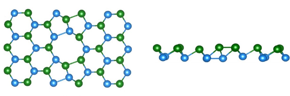
Adalberto Fazzio: Whenever we reflect on the main contributions in a given area, we look at the most cited articles, which do not always correspond to the articles that the authors would expect to be the most cited. But I will try to give you a brief description of some of the themes in which I believe I made a contribution that was highlighted. In the study of defects and impurities in semiconductors, I highlight the study of transition metals (TM) in semiconductors. At the time – until 1984 – there was a wealth of experimental data concerning the position of levels of impurities in the gap and the optical excitations of all MT-3ds. And the theoretical calculations based on a medium-field theory did not explain these data. During my post doctoral research at NREL (National Renewable Energy Laboratory) in 1983/84, we developed a model to describe the experimental data. It was a model that coupled the field crystal theory with the DFT theory, which described effects of multiplets from the TM impurities. Several articles were published applying this model. The model is presented in detail in Phys. Rev. B 30, 3430 (84). This work was in collaboration with the researchers Alex Zunger and Marilia Caldas. And those results led to a letter in the Appl. Phys. Lett. (1984) which would be of great interest to experimental physicists, titled “A Universal trend in the binding energies of deep impurities in semiconductors”. A major change occurred in this area in the late 1980s, with the “Large Unit Cell” calculations, DFT method and pseudo potentials. Today known simply as “ab initio methods” or “free parameters”. Regarding this development, I was at the Max Planck Institute in Berlin, working with Matthias Scheffler. Together with my doctoral students (T. Schmidt and P. Venezuela), we were pioneers in the use of this type of methodology in Brazil, widely used until now. After these studies, I started working with amorphous systems. Since we could now work with systems containing many atoms per unit cell, we decided to couple the ab initio calculations using structures generated by Monte Carlo simulations. I highlight two papers: one in a-SiN (PRB, 58, 8323 (1998)) and a-Ge:N (PRL 77, 546 (96)).
At the end of the 1990s, at the Brazilian National Synchrotron Light Laboratory (LNLS), Professor Daniel Ugarte was performing beautiful experiments with HTEM, where he observed the formation of linear chains of atoms in Au and Ag fine films. Our group at USP, in cooperation with Edison Zacarias at UNICAMP, had begun studies to understand the formation of linear chains of Au atoms. Some of the questions were about how these chains broke and how we could explain the great distances that appeared between atoms. This experiment-theory interaction was a very important moment. Several papers were published, one which was widely cited “How do gold nanowire break?” (PRL 87, 196803 (2001)). This work was the cover of PRL and highlighted by the editor of Science. And later we showed how oxygen acts to trap the Au atoms in the wires (PRL 96, 01604 (2006)) and the effects of temperature and quantum effects on wire breakage and stability, important aspects to understand the observations (PRL 100, 0561049 (2008)).
In the same period, our group at USP focused on the study of nanostructures of carbon, silicon, etc. Although we had strong tools for describing electronic, magnetic, optical and mechanical properties, the understanding of these materials lacked the properties of electronic transport. In this context, we developed a computational code based on the Landauer-Büttiker theory. Several PhD students were involved in this code, which is known as TRANSAMPA. And, in my opinion, several important works were carried out to better understand the behavior of electronic transport properties. To exemplify this, we were pioneers in describing the transport in doped graphene tapes (PRL 98,196803 (2007)). I should also mention the collaboration with Professor Alexandre Reilly from IFT (Institute of Theoretical Physics of UNESP) who was then a post-doc, which resulted in a very important improvement of this code, and which allowed to treat materials with the realistic dimensions used in the experiments. In 2008, in a paper titled “Designing Real Nanotube-based Gas Sensor” (PRL 100, 176803), we showed how nanotubes can function as realistic-sized sensors, with defects. Using first-principle calculations, we had systems of micrometric dimensions within our reach.
Currently, my research is more focused on the search for devices formed by 2D materials whose interface is primarily built by van der Waals interactions. For example, like graphene, a new 2D material was isolated from exfoliated black phosphorus, also called phosphorene. We studied the graphene/phosphorene interface (PRL 114, 066803(20015)), showing how a device can be constructed.
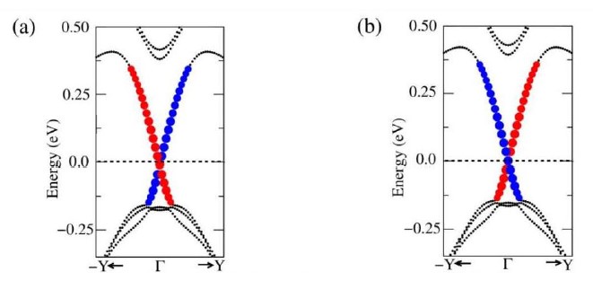
Another class of materials I have been working on concerns the well-known topological insulators. A Topological Insulator (TI) is a material that has no states of energy gap “at the edges” and whose “bulk” is insulating! These states are topologically protected and robust against disturbances. In the case of two-dimensional (2D) materials (2D), they are known as insulators that feature Quantum Spin Hall (QSH). The scattering surface state is protected by time reversal (TR) symmetry, leading to an electronic transport without energy dissipation. In 2011, together with the UFU group, we showed how magnetic impurities in topological insulators have their spin texture modified (PRB 84, 245418 (2011)). Recently, in collaboration with Professor Zhang from the Rensseler Polytecnic Institute, we presented a general model for describing the topological/trivial interface. We showed, for example, the Bi2Se3/GaAs interface. There were replicas of the Dirac cone that emerged from the interface interaction including semiconductor states (Nature Comm. 6, 7630(2015)). Phosphorene is a 2D material that has semiconducting properties. In cooperation with the group of Professot Alez Zunger, of the University of Colorado, we studied this material under the action of an electric field and showed that for three or four layers of phosphorene, under the action of the field, it has a topological transition (NanoLett. 15, 1222 (2015)).
Finally, I would like to mention an activity that I am initiating, which is the use of Machine-Learning techniques for material properties. In particular, I have focused on topological insulators. And as I mentioned earlier, specifying the more relevant studies I have left out many others.
As for other types of contributions, together with José Roque I built a very productive group at IF-USP, known as SAMPA (Simulation Applied to Materials – Atomic Properties) where numerous doctors and masters, and several postdocs were cultivated. I should add that all this was possible mainly due to the support of Fapesp, via thematic projects. I was head of the Department of Materials Physics, Director of IFUSP and pro tempore Director of the Federal University of ABC. From a management point of view, I would like to highlight my participation at the Ministry of Science, Technology and Innovation, where I was the Under-Secretary of Setec (Technology and Innovation Secretariat) and SCUP (Secretariat of Research Units). And I am proud to have coordinated the creation of the Brazilian Nanotechnology Initiative, where the SISNANO system is an important arm – a set of laboratories dedicated to technological research and development.
I also wrote two books that have been adopted: “Introduction to Group Theory: applied in molecules and solids”, together with Kazunori Watari and “Quantum Theory of Molecules and Solids”, together with José David Vianna and Sylvio Canuto.
SBPMat Bulletin: You have just taken on the direction of the Brazilian National Nanotechnology Laboratory (LNNano). Please share with the Materials community your plans for LNNano. How do you see the situation of nanoscience and nanotechnology research in Brazil given the recent budget cuts?
Adalberto Fazzio: Two weeks ago I took on the direction of the National Nanotechnology Laboratory (LNNano), one of the four National Laboratories of the National Center for Research in Energy and Materials (CNPEM). This is a laboratory recognized for its excellence, dedicated to the production of knowledge in nanotechnology, moving from basic science to technological innovation.
I was very happy and I hope to continue the work of the researchers who were at the forefront of LNNano and who preceded me, such as Daniel Ugarte, Fernando Galembeck and Marcelo Knobel. This is the laboratory that holds a management bond with MCTIC fully dedicated to nanotechnology. One of its main missions is to service external users through open equipment. An example is the electron microscopy and probes park, which is certainly the best equipped in Latin America. LNNano is the main executor of government policies in the area. We have intense in-house mission-oriented research activity with impact studies. We are currently undertaking minor restructurings to better serve external users and to strengthen ongoing research.
The nanotechnology platform has raised considerable resources in all developed countries of the world. For example, the US government has annually deposited something in the order of US$ 1.8 Bi. Unfortunately, in Brazil we have had difficulties to provide continuity to even much more modest programs. However, the community has responded with great capability to the development of nanotechnology products. Today, for example, anchored in the SISNANO system, we have about 200 companies seeking innovation in the Nano area; and in particular, the performance of LNNano has been outstanding.
What we cannot however, is face budget cuts in science and technology every year. We are in a very delicate moment in our economy, low growth, but it is imperative to preserve the achievements of the last decades in the area of science and technology. The programs in the area of research and technology development must be preserved. This is because when the crisis is over, the country must be prepared to continue growing. Therefore, it is fundamental to continue generating new knowledge, striving for technological innovation and also training qualified human resources. In other words, the economic slowdown should not be accompanied by investment cuts in technology and development research.
SBPMat Bulletin: Please leave a message for the readers who are starting their scientific careers.
Adalberto Fazzio: The greatest wealth in our country is human capital. Brazil has a large young population, young people who are often in the middle of the path in their scientific and technological careers, because they are not able to envision in the future the acknowledgment and respect for a fundamental activity, which is the search for knowledge. Those who desire to pursue a scientific career must persevere and stand firm in their studies.