Featured paper: Isolating nanoribbons with conducting regions.

[Paper: Topologically Protected Metallic States Induced by a One-Dimensional Extended Defect in the Bulk of a 2D Topological Insulator. Erika N. Lima, Tome M. Schmidt, and Ricardo W. Nunes. Nano Lett., 2016, 16 (7), pp 4025–4031. DOI: 10.1021/acs.nanolett.6b00521]

Isolating nanoribbons with conducting regions

A research carried out in Brazil made an important contribution to the study of topological insulators, a class of materials that was theoretically predicted in 2005 and experimentally confirmed in 2007. The study was reported in an article recently published  in Nano Letters (impact factor: 13.779).

A unique property of Topological insulators is that they behave as insulators on the inside and as conductors on its surface or edge. According to Ricardo Wagner Nunes, professor at the Federal University of Minas Gerais (UFMG) and corresponding author of the article, “non-topological insulators may also have conductive surfaces, but in the case of topological insulators, conduction of charge and spin on the surface is robust, as it is “protected” by time reversal symmetry”.

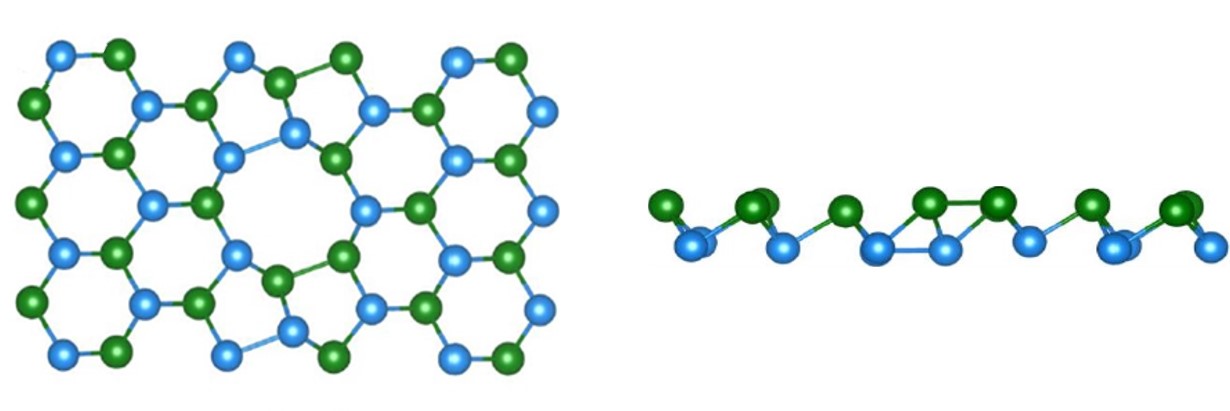
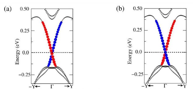
In the article in Nano Letters, Professor Nunes and colleagues, Erika Lima, of the Federal University of Mato Grosso (UFMT) – Rondonópolis campus, and Tome Schmidt, of the Federal University of Uberlândia (UFU), reported their work on a two-dimensional topological insulator, a bismuth nanoribbon of only two layers of bismuth atoms (one-atom thick), superimposed and bonded. Using computational methods, the scientists showed that the interior of the bismuth nanoribbon, instead of being fully insulating, may have conductive states (also called metallic states) generated from a particular type of irregularity in the atomic structure of the material, known as 558 extended defect.

Representation of bismuth bilayer nanoribbon with the defect 558, top view (left) and side view (right). The green balls represent the atoms of the top layer of the material and the blue balls, the atoms of the lower layer. In the center of the left figure, the defect is clearly seen: pentagons and an octagon stop the repetition of the hexagons.


“In our work, we show that a linear defect within a two-dimensional topological insulator can generate one-dimensional electronic quantum states that conduct spin and charge within the material”, say the authors.

This conclusion was supported through calculations performed on supercomputers, simulating what would happen to the electrons in quantum states, in the material, in the presence of defects. “We used first-principles Density Functional Theory calculations”, specify the authors, who relate that the computer simulation of defects in bismuth nanostructures required approximately 400 hours of computer simulations on supercomputers in the Department of Physics – UFMG and at the National Center for High Performance Computing in São Paulo (Cenapad) – UNICAMP.

A figura mostra a curva de dispersão dos estados topológicos metálicos, localizados no defeito 558, marcados em azul e vermelho.
The figure shows, marked in blue and red, the dispersion curve of the metal topological states located in the defect 558.

In the article, the authors also propose the existence of pentaoctite, a new two-dimensional topological insulator. This material, which has not been synthesized yet, is a bismuth bilayer with a crystal lattice formed by atoms arranged in pentagons and octagons. As stated by the authors, “In our calculations we show that this new “phase” of the two-dimensional bismuth has low formation energy, which opens the possibility to be synthesized in the laboratory”.

According to the authors, the work reported in Nano Letters raises several issues in the scope of fundamental research, such as the influence of magnetic and non-magnetic impurities on the spin and charge transport in the proposed topological states, and the connection between the network symmetries and nature of the topological edge states on pentaoctite. “From the point of view of applications, it would be interesting if our work could motivate experimental studies of two-dimensional topological insulators based on bismuth and other materials, enabling theoretical and experimental collaboration on this issue”, comment the authors, leaving an open invitation to experimental research groups.

The origin of this research work

“The work originated by combining my interest in extended topological defects in two-dimensional and three-dimensional materials, with the experience of Professor Tome Mauro Schmidt (UFU) and Erika Lima, his doctoral student in the subject of topological insulators”, states Nunes.

In 2012, Nunes and collaborators published an article in Nano Letters on magnetic states (non topological) generated by linear extended defects in a monolayer of graphene. Later, in a conversation with Schmidt, a collaboration was decided in order to investigate if an extended defect with the same morphology would lead to the formation of topological states in a bidimensional topological insulator made of bismuth.

In her post-doctorate in the group of Professor Nunes, in 2015, Erika Lima performed all computer calculations. The three researchers, who are the authors of the article, interpreted the results and wrote the paper.

The research that led to the article received funding from Brazilian agencies CAPES, CNPq, FAPEMIG and from the National Institute of Science and Technology on Carbon Nanomaterials.

autores
Photos of the authors. From left to right, Erika Lima, currently a professor at UFMT, Tome Schmidt, professor at UFU, and Ricardo Nunes, professor at UFMG.

SBPMat newsletter. English edition. Year 1, issue 9 – special: XIII SBPMat Meeting.


Brazilian Materials Research Society (SBPMat) newsletter

News update from Brazil for the Materials community


English edition. Year 1, issue 9. 

Greetings, .

Final arrangements for our meeting in João Pessoa!

– Read the message of the chairs of the event, which this year accepted 2,141 papers and has nearly 2,000 registrations from 28 countries so far. In the message, professors Ieda Garcia and Severino de Lima show the highlights of the program of this year’s meeting! Here.

– After lunch and before the afternoon plenary lectures, you can attend technical lectures of the meeting´s sponsors in João Pessoa: Shimadzu/Tescan will discourse about SEM with ion beam and TOF SIMS detector, and FEI will address DualBeam TEM. Learn more.

– Why is João Pessoa called “the sun door“? Learn more about the city, one of the oldest in Brazil, and its natural and cultural features. And get ready to dive into green waters at 28 °C! Read about João Pessoa.

– What to pack? Track the weather, whose temperatures should be between 20 °C and 30 °C. But pay attention, the meeting organization warns that, at the Convention Center, the air conditioner will make the room fresh … Link to weather in João Pessoa.

– Registration: here.

Program at a glance: here.

Detailed schedule. Search for times and locations of symposia presentations: here.

–  Some options of accommodation, car rental, transfers from the airports of the region, transportation from hotels to convention center, and tours: see on the home page of the site of the event.

– And what about the conference party? This year, it will be held on Wednesday evening at Espaço Caixa Econômica Federal in Cabo Branco. Tickets may be purchased in the information desk as of Monday 1 p.m..


Interviews with our plenary speakers

We interviewed Robert Chang, professor of the first department of Materials Science in the world at Northwestern University. Besides having a remarkable career as a researcher (his H index is 56), “Bob” has dedicated the past 20 years guiding the development of the Materials World Modules program, which develops educational, interactive and playful material (for example, card games) on Materials and Nanotechnology for pre-college students and their teachers. In his plenary lecture at the XIII SBPMat Meeting, Professor Chang will try to mobilize citizens of the world to solve global problems together. See our interview with the scientist.

We also spoke with Professor Colin Humphreys, a professor at the University of Cambridge.  Among other honors, the scientist was knighted by the Queen of England for his services to science. Besides being the author of over 600 publications, the professor developed materials for the industry that currently fly in aircraft engines and created low cost LEDs based on gallium nitride, material on which he specialized. In João Pessoa, he will show, among other issues, how gallium nitride could reduce electricity consumption by 25% in the world. See our interview with Colin Humphreys.


We interviewed the German physicist Karl Leo, specialist in organic semiconductors. Beyond being the author of more than 550 papers with more than 23,000 citations and 50 families of patents, the scientist has already participated of the creation of 8 spin-off companies. In his lecture at the XIII SBPMat Meeting, Karl Leo will speak on highly efficient organic devices, as OLEDs and solar cells. See our interview with Karl Leo.

We also spoke with the Portuguese physicist Antonio Luis Ferreira Martins Dias Carlos, of the University of Aveiro, who will perform a lecture in our meeting in João Pessoa on luminescence applied to nanomedicine. In the interview, the professor shared with us his most prominent works in the field of Materials. He also told us about some challenges in the area of luminescence for medical applications, both in medical imaging and intra-cellular temperature mapping, and cited examples of applications of luminescent materials that have already been used in the diagnosis and treatment of various diseases. See our interview with Luis Dias Carlos.


We interviewed the French scientist Jean-Marie Dubois (Institut Jean-Lamour), specialist in quasicrystals (ordered, but aperiodic structures on solid materials) and pioneer in patenting applications for them. He told us a little about his main contributions to the field of Materials and gave a teaser on the theme of his plenary lecture in the XIII SBPMat Meeting: he will talk about quasicrystal structures, found in metallic alloys, polymers, oxides and artificial nanostructures, and their unprecedented properties. In the picture, Jean-Marie Dubois (on the left) and Dan Shechtman, who received a Nobel Prize in 2011 for the quasicrystals, using equal ties, both decorated with the Penrose tiling, an example of aperiodicity.  Read our interview with Jean-Marie Dubois here.

We also interviewed the Italian chemist Roberto Dovesi (Universita’ degli Studi di Torino), one of the creators of CRYSTAL, a computational tool for ab initio quantum calculations used in the study of several solid materials properties. The CRYSTAL code is currently used in over 350 laboratories around the world.  In his plenary lecture in the XIII SBPMat Meeting, Dovesi will attempt to demonstrate that today quantum simulations may be very useful tools to complement experiments. See our interview with Roberto Dovesi.


We have interviewed Professor Alberto Salleo, from Stanford University, who is going to give a plenary lecture on organic electronic devices in the XIII SBPMat Meeting. Young, yet holding a career that stands out internationally, Salleo told us about the work conducted by his group, which has been developing a deeper understanding on the role provided by the defects in charge transport in organic semiconductors. He also shared with us his main papers, published in Nature Materials. Finally, Salleo discussed the next challenges and applications on organic electronics, and anticipated what he is going to address in the plenary lecture, which promises to be very informative while mild enough for a wider audience. Read our interview with Alberto Salleo.

To suggest news, opportunities, events or reading recommendations items for inclusion in our newsletter, write to comunicacao@sbpmat.org.br.
Unsubscribe here.