|
|||||||||||||||||||||||||||||||||||||||||||||
|
|||||||||||||||||||||||||||||||||||||||||||||
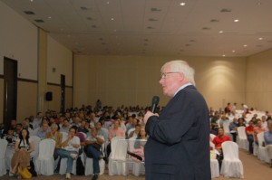
The scene repeated itself daily while the event lasted: around 8.30 a.m. and 2 p.m., under the strong João Pessoa sun, lines of hundreds of participants entered the convention center and settled at the refrigerated plenary room. There, scientists with outstanding careers, attested by their H indexes of values ranging from 40 and 73, coming from England, France, Germany, Italy, Portugal and United States, shared their knowledge about matters on which they are, without a shadow of a doubt, qualified specialists.
In the event’s final plenary lecture, Robert Chang, professor at the first department of materials science in the world, at Northwestern University, resumed two subjects that had been explained by Professor Arana Varela in the memorial lecture, and which permeated almost every plenary. The first one is the essential role that materials field and, in particular, nanotechnology play in meeting, in a sustainable way, the needs and demands of humanity in healthcare, food, transportation, security and communication. The second subject is the need for collaboration to face this challenge of the 21st century.
In this context Chang, who was president of the American Materials Research Society (MRS) and founded in 1991 the International Union of Materials Research Societies (IUMRS), called upon the young Brazilians [see video below] to be part of a global network released in 2012, which promotes the interaction of young researchers in the field around these global challenges through a biennial conference and virtual platforms.
However, Chang said, the scientific collaboration among physicists, chemists, engineers, mathematicians, biologists and other researchers to develop the necessary technologies is insufficient. It is also necessary, he added, to rely on the collective, global effort from governments, companies, communities, families and individuals to deploy these technologies on peoples’ daily lives. “That requires education”, he said. For the last 20 years, the scientist has conducted the Materials World Modules Programme, which developed interactive educational material about Materials and Nanotechnology for middle and high-school students.
Nanomedicine
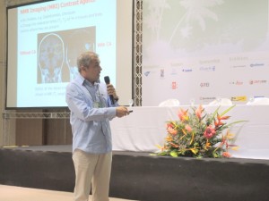
Portuguese professor Luís Carlos, from the University of Aveiro, brought to XIII SBPMat Meeting many examples about the applications of nanotechnology in the healthcare field that are making a difference, or may make a difference in the short-term.
Being an expert in luminescent materials, which emit light not derived from heat, the scientist showed in his plenary lecture that these materials are already of great use in medical diagnosis. Luminescent organic complexes, for example, are marketed as contrast agents for magnetic resonance imaging, and as markers for fluoroimmunoassays (used in pre- and neonatal screening and detection of proteins, viruses, antibodies, drug residues etc.).
Besides, Luís Carlos said, luminescent nanoparticles (quantum dots and nanocrystals with lanthanide ions) emerge in diagnostic techniques and also in treatments, such as the hyperthermia process. This consists in the exposition of biological tissues, usually cancerous cells, at temperatures above 45°C, causing their deaths, with minimum collateral lesions to surrounding normal tissues. With proper temperature monitoring and control, the technique can soon become popular.
For the last few years, there have been efforts to develop nanothermometers that measure intracellular temperature to service this and other applications, not only regarding Nanomedicine, but also in fields such as Microelectronics, Photonics and Microfluidics. A successful example, presented by Luís Carlos at the plenary, is the development of a nanometric platform composed by nanorods, which work as thermometers, with gold nanoparticles on its surface, which function as heaters. This is a platform that, in contrast to its small size, can bring great benefits to the improvement of the technique of hyperthermia and the study of the processes of heat transfer at the nanoscale.
LEDs and other gallium nitride devices: savings of 25% in the global electricity consumption
When the Nobel Prize in Physics was announced for three Japanese scientists whose works were essential for the development of LED white light bulbs, those who had participated in XIII SBPMat Meeting certainly remembered the plenary lecture by Sir Colin Humphreys from University of Cambridge. The material chosen by the laureates when they decided to face the challenge of creating the blue LED that would allow the white light emitting LED was gallium nitride, which was also the object of Sir Colin’s lecture.
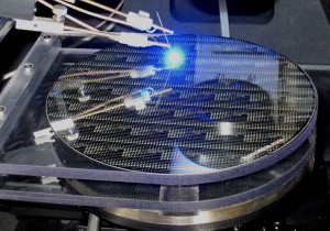
Professor Humphreys is an expert in this material. He created and directs a research center in Cambridge devoted to gallium nitride, and he also founded two spinoff companies to commercially exploit the technology developed by his research group and manufacture LEDs grown on relatively large silicon wafers, of about 15 cm, for low cost lighting. In 2012, the spinoffs were purchased by Plessey, a manufacturer of products based on semiconductor materials with over 50 years in the market. Now these LEDs are produced by Plessey in the United Kingdom.
The gallium nitride LED bulb currently offers one of the longest shelf lives in the market – 100,000 hours of use, equivalent to 69 years without switching the bulb, against 1,000 hours of life of the incandescent light bulb and 10,000 of the fluorescent. These LEDs also provide high energetic efficiency, ranging from 100 to 200 lumens (amount of light emitted in a second) per watt of power consumed.
At the plenary lecture, Sir Colin showed that the widespread use of LEDs in lighting would result in savings of about 15% in the total electricity consumed on the planet, and thus in a substantial decrease in emissions of carbon dioxide. In fact, lighting is one of the few segments where devices with high-energy efficiency are not yet universal.
More energy can be saved, Professor Humphreys said, by replacing silicon by gallium nitride in various electronic devices. In total, Humphreys concluded, up to 25% of all electricity used in the world today could be saved, reason why, added to the other applications of gallium nitride in the healthcare field, it was enough for the British scientist to state that this manmade material is one of the most important in the world.
Organic semiconductors: OLEDs and solar cells in the spotlight
Just like it happens with LEDs, the OLEDs, which are manufactured with organic materials justifying the “O” in the acronym, directly convert electricity into light and are, therefore, devices with high potential efficiency, which has been improved every year. Having each one particular advantages, LEDs and OLEDs already compete in certain markets, such as the one of displays and, in a more incipient manner in the case of organics, in the lighting market.
Along with organic solar cells, OLEDs were the focus of Karl Leo’s plenary lecture. He is a professor at the German TU Dresden and at the Saudi Arabian KAUST universities, and wrote over 550 papers with 23,000 references and 50 patent families. He is also founder of 8 spinoff companies, such as Heliatek and Novaled, which manufacture organic solar cells and OLEDs, respectively.
Professor Leo showed an important quantity of results achieved by his research groups, regarding the improvement of organic semiconductor devices. Along with his collaborators, Karl Leo has developed an extensive work about doping organic semiconductors in the transport layers of OLEDs and solar cells to increase significantly their electrical conductivity. This work resulted, for example, in obtaining white light-emitting OLEDs with energetic efficiency greater than those of fluorescent tubes.
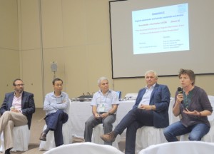
Karl Leo was not the only internationally renowned scientist in João Pessoa in the field of organic semiconductors. On Wednesday afternoon, a roundtable organized by Symposium D gathered four of these specialists: Alberto Salleo (Stanford University), Franky So (University of Florida), Heinz von Seggern (TU Darmstadt) and Jenny Nelson (Imperial College London). Moderated by a prominent Brazilian scientist of the field, Roberto Mendonça Faria, professor at the São Carlos Institute of Physics at University of São Paulo and SBPMat president, the session gathered dozens of participants of the meeting, of various ages, that actively participated at the debate.
The discussion was around the challenges of organic electronics, from basic research to mass production (or individual production, as pointed out by a young man of the public drawing attention to the 3D printing techniques). Various subjects of the scientific, industrial and social fields were addressed bythe panelists based on the audience’s questions. “Fortunately, there are challenges for Materials Science. Unfortunately, there are challenges for mass production,” Professor Faria summed up, resuming, somehow, one of the first lines of the round table, in which Professor Jenny Nelson lamented that the scientific community celebrated a lot more the development of a device that works than the understanding of why a particular device did not work.
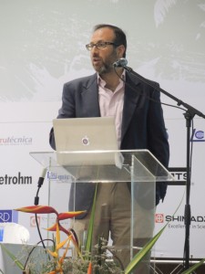
Alberto Salleo, creator of a group in Stanford that studies the relation between structure and properties on polymeric semiconductors to better understand the charge generation and transport, also delivered a plenary lecture at the event. In the lecture, Salleo cast doubt on the universality of a widespread assumption that links a high degree of crystallinity (or order) in the microstructure of these polymers to a higher charge mobility, or better performance of the devices. The scientist showed that the disorder is good for organic solar cells and cited examples of almost amorphous semiconducting polymers having similar performance to others much ordered.
Professor Salleo presented a model developed by his group to show how the charge transport in organic semiconductors works, since they are materials with heterogeneous microstructures, where disordered and ordered aggregates coexist with each other and with long polymer chains. In order to have high charge mobility, Salleo revealed, the important thing is for the aggregates to connect among themselves, which happens through the polymeric “spaghetti”.
Order, but without periodicity
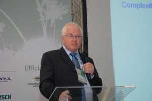
The quasicrystals are far from the disorder, but also outside the traditional crystalline order. These materials were the general theme of the plenary of French researcher Jean-Marie Dubois, from Institut Jean Lamour, whose experience in this field was recognized by the scientific community through the creation of the “Jean-Marie Dubois International Award”, given every three years to research works related to quasicrystals.
First, Dubois presented an introduction to quasicrystals, materials in which the atoms are grouped into unit cells in patterns which are ordered (which may be determined by algorithms) but not periodic (never repeat themselves). Beautiful scientific and artistic images intermixed in Dubois’ presentation allowed the audience to view this aperiodic order.
The lecturer also paid homage to Dan Shechtman, who discovered quasicrystals in 1982 and, after many fights and resistance in the scientific community, eventually won the Nobel Prize in Chemistry in 2011 and generated a big shift in the vision of ordered condensed matter. Today, quasicrystalline materials are synthesized and used in various products, such as auto parts and pans, to improve their thermal conductivity, adhesion, friction, corrosion resistance etc. It is noteworthy that Dubois is among the pioneers in filing patents targeting applications of quasicrystals.
The quasicrystalline order can be observed in various types of materials. In the lecture at the XIII SBPMat Meeting, Dubois addressed, in particular, metal alloys formed by three elements (A, B and C), in which A – B and B – C form chemical bonds, while B and C repel themselves. Named by Dubois “push-pull alloys”, these materials can form very complex intermetallic compounds, with up to hundreds of atoms per unit cell. Among these, only a few can further increase their complexity to form a quasicrystalline order, which results in unique properties and open up possibilities for new applications.
Computer simulation
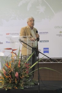
In another plenary lecture of the XIII SBPMat Meeting, supporters of computer simulation as a complement to the experimental work in the investigation of material properties, and those interested in using it, were able to hear from Professor Roberto Dovesi (Università di Torino) that this dual approach is worthwhile.
Dovesi is one of the creators of CRYSTAL, a computational tool that allows the characterization of crystalline solids from the point of view of quantum mechanics, through ab initio calculations. The first version of the program was developed from 1976 onwards and released in 1988, making CRYSTAL the first periodic code distributed publicly to the scientific community. Now in its seventh version, the program allows the study of elastic, piezoelectric, photoelastic and dielectric properties, polarizability and hyperpolarizability tensors, IR and RAMAN spectrum, structure of electronic and phononic bands, among other properties.
The Italian chemist highlighted the affordable price and high working speed of today’s computers that are suitable to run such programs. As an example, he cited a machien recently acquired by his research group for computer simulation, which, costing around 6,500 euros, is able to do long calculations in a few hours with its 64 cores. Supercomputers are not necessary, Dovesi said, and are less robust. As for software, Dovesi remarked that today the field of materials has powerful, robust, easy-to-use programs at affordable prices (a basic license of the latest version of CRYSTAL, for example, costs 600 euros.
|
||||||||||||||||||||||||||||||||
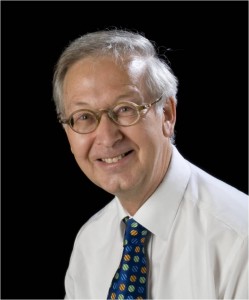
Sir Colin Humphreys, PhD from Cambridge and a BSc from Imperial College, is Professor of Materials Science and Director of Research in the Department of Materials Science and Metallurgy at the University of Cambridge (United Kingdom). His research covers three main areas: gallium nitride (GaN) materials and devices, advanced electron microscopy, and ultra-high temperature aerospace materials. He has published hundreds of papers on electron microscopy and given many plenary and invited lectures throughout the world. He has received national and international medals for his research in electron diffraction and microscopy and on gallium nitride.
He founded a spin-off company (CamGaN) to exploit the research on gallium nitride of his group on low-cost LEDs for home and office lighting. The company was acquired in February 2012 by Plessey, which manufactures LEDs based on this technology. He is the founder and director of the Cambridge Centre for Gallium Nitride, a center with world-class growth and characterization facilities where research is carried out from fundamental studies on GaN to applications in LEDs and lasers. He also founded and directs the Cambridge/Rolls-Royce Centre for Advanced Materials for Aerospace, which developed materials that now fly in Rolls-Royce engines.
He is a fellow of the Royal Society, the self-governing Fellowship of many of the world’s most distinguished scientists drawn from all areas of science, engineering, and medicine, and of the Royal Academy of Engineering. He is also a fellow of Selwyn College, one of the Cambridge University 31 autonomous units in which students live, eat, socialise and receive some teaching sessions. In 2010 he was Knighted (receive a special honor and the title of Sir from the Queen of England) for services to science.
Professor Humphreys has authored over 600 peer reviewed papers with over 9,400 citations and his h-index is 43.
In his limited spare time he writes books on science and religion, such as “The Mystery of the Last Supper: Reconstructing the Final Days of Jesus”, which has recently been translated into Russian, German, Portuguese, Japanese and Greek.
Read our interview with the plenary speaker.
SBPMat newsletter: – Why do you think gallium nitride is one of the most important semiconductor materials? Which are the main challenges in the field of gallium nitride for materials scientists and engineers?
Sir Colin Humphreys: – I think gallium nitride is one of the most important semiconductor materials because of the huge range of potential applications and the benefits to mankind which will result from these applications. The main challenges to realising these applications are reducing the cost of GaN devices and improving the efficiency still further.
SBPMat newsletter: – Which are the principal contributions you have done for the development of Materials Science and Engineering?
Sir Colin Humphreys: – The principal contributions I have made for the development of Materials Science and Engineering are solving some fascinating problems in basic science and also developing materials for industry. For example, I direct a Rolls-Royce Centre in Cambridge on Advanced Materials, and some of the materials we have developed are now flying in Rolls-Royce engines. In addition, I direct the Cambridge Centre for Gallium Nitride, and the low-cost GaN LEDs on silicon that we developed are now being manufactured in the UK by Plessey.
SBPMat newsletter: – Brazil is making efforts to transfer technology to the industry. You have founded a spin-off company and research centers, in both cases having good technology transfer results. Based on these experiences, what would you say to the Brazilian Materials community about making technology transfer real?
Sir Colin Humphreys: – First, scientists and engineers have to have an idea for a new or better product. In order to convince industry, it is important that the scientists and engineers make prototype devices to show to industry. If the scientists and engineers decide to set up their own company, it is usually helpful to bring in a CEO from outside to run the company because most scientists and engineers are not so good at running a company. The choice of the CEO is critical. It is also possible to set up a company for virtually nothing, set up a website for virtually nothing, etc. It is really important to get lots of good advice. I was fortunate in setting up two companies, in that I got a lot of good advice for free because there are a lot of people around Cambridge in the UK that have set up companies and can give good advice. Finally, making technology transfer real is good fun, but also hard work! You may have lots of set-backs, but keep persevering! Also, be enthusiastic about your product, if you are not enthusiastic, no-one else will be! You have really to believe in what you are doing.
SBPMat newsletter: – If possible, tell us a little about the topic of your plenary talk at SBPMat meeting.
Sir Colin Humphreys: – In my plenary talk at João Pessoa I plan to start by showing some striking atomic-resolution electron micrographs showing single silicon impurity atoms in graphene, and showing that they can occupy two different sites. I will also show images of dancing silicon atoms in graphene (I know Brazilians are experts in dancing!). I will then move on to talk about Gallium Nitride (GaN) and how this amazing man-made material is likely to save more energy and CO2 emissions than solar, wind-power and biomass together! I will describe how advanced electron microscopy and atom probe tomography have been used to solve the fascinating problem of why GaN LEDs are so bright when the dislocation density is so high. I will also describe how growing GaN LEDs on large area silicon substrates can substantially reduce the cost of LEDs, and this cost reduction is likely to enable GaN LEDs to be the dominant form of lighting in our homes, offices, streets, etc, in the near future. In addition, I will show how GaN-based power electronic devices are 40% more efficient than silicon power electronic devices, so replacing Si power electronics by GaN would save another 10% of electricity, on top of the 10-15% electricity savings from using GaN LEDs. So GaN could potentially save 25% of the world’s electricity consumption, which is amazing.
In addition to saving energy and carbon emissions, if aluminium is added to GaN, then deep-ultra-violet (UV) light is emitted and this can kill all bacteria and viruses. So such deep-UV LEDs could be used for water purification in the world, saving millions of lives. Finally I will talk about how optimised quality LED lighting can improve the health of all of us and the exam results of school children! My talk will range from basic science through to applications.
O artigo científico de membros da comunidade brasileira de pesquisa em Materiais em destaque neste mês é:
Wan Ki Bae, Young-Shin Park, Jaehoon Lim, Donggu Lee, Lazaro A. Padilha, Hunter McDaniel, Istvan Robel, Changhee Lee, Jeffrey M. Pietryga & Victor I. Klimov. Controlling the influence of Auger recombination on the performance of quantum-dot light-emitting diodes. Nature Communications 4, article number 2661, published 25 October 2013. doi:10.1038/ncomms3661.
Texto de divulgação:
Pontos quânticos desenvolvidos para LEDs mais eficientes
Um trabalho de pesquisa publicado no mês de outubro na Nature Communications, revista científica de conteúdo aberto do grupo Nature, resultou num material que aumenta dezenas de vezes a eficiência de LEDs de pontos quânticos ao diminuir a influência do efeito Auger, um dos principais limitadores da eficiência desses dispositivos que apresentam grande potencial para serem usados em iluminação, entre outras aplicações. O trabalho foi realizado no Grupo de Nanotecnologia e Espectroscopia Avançada do Laboratório Nacional de Los Alamos, localizado no sul dos Estados Unidos, com a participação de um doutor brasileiro, Lázaro Padilha, e com a colaboração de grupos da Coreia.
“O resultado veio depois de mais de um ano de pesquisa sobre como efetivamente minimizar o efeito Auger em pontos quânticos”, relata Padilha, atualmente professor do Instituto de Física da Unicamp, que chegou a Los Alamos em 2010 para fazer um estágio de pós-doutorado. O trabalho que gerou o paper na Nature Communications, além de outros artigos em periódicos de alto fator de impacto como Nano Letters e ACS Nano, começou no final de 2011 e, na sua primeira etapa, visou entender o processo físico para minimizar a influência do chamado “efeito Auger” ou “recombinação Auger” nos pontos quânticos.
Os pontos quânticos, cristais semicondutores de alguns nanometros de tamanho, apresentam propriedades que possibilitam a emissão de luz com brilho intenso e cores puras e podem ser fabricados usando técnicas simples e de baixo custo. Por esses motivos, essas nanopartículas são materiais interessantes para a fabricação de LEDs. Desde a primeira demonstração de LEDs de pontos quânticos, ocorrida em 1994 (Nature 370, 354 – 357, 04 August 1994; doi:10.1038/370354a0), esses dispositivos têm sido objeto de pesquisas visando otimizar sua capacidade de converter eletricidade em luz.
Nos LEDs, a emissão de luz se produz quando, ao se introduzir energia no dispositivo por meio de corrente elétrica, ocorrem recombinações nos átomos do material emissor. Especificamente, elétrons próximos ao núcleo do átomo saem de seu lugar deixando vagas, as quais são preenchidas por elétrons mais distantes, dotados de mais energia. A energia excedente pode sair em forma de fóton, ocorrendo a desejada emissão de luz, ou pode ser transmitida a um terceiro elétron, que será ejetado do átomo. Esta segunda possibilidade constitui o efeito Auger, que pode ser visto como um concorrente da emissão de luz no uso da energia.
Nanoengenharia dos pontos quânticos
Depois de compreender como minimizar a recombinação Auger nos pontos quânticos do ponto de vista físico e constatar que impacta significativamente na eficiência dos LEDs, o grupo de Los Alamos se propôs a desenvolver o material que teria o melhor desempenho frente a esse efeito. “Eu trabalhei nos estudos de espectroscopia para entender os processos físicos que levariam a um melhor desempenho dos materiais como base para LEDs”, diz Lázaro Padilha.
O desenvolvimento do material foi feito a partir de pontos quânticos compostos por um núcleo de seleneto de cádmio (CdSe) e uma casca de sulfeto de cádmio (CdS). Para conseguir a redução da influência do efeito Auger, os cientistas aplicaram duas estratégias de nanoengenharia: a variação da espessura da casca e a introdução de uma camada composta por uma liga de zinco, cádmio e enxofre (ZnCdS) entre o núcleo e a casca.
Após concluir, em Los Alamos, o desenvolvimento do material base, os colaboradores da Coreia do construíram LEDs com uma arquitetura na qual a camada emissora, formada pelos pontos quânticos, ficou inserida entre as camadas de transporte de cargas negativas e positivas, sendo uma inorgânica e a outra orgânica, respectivamente, como mostra a figura a seguir, extraída do artigo da Nature Communications:
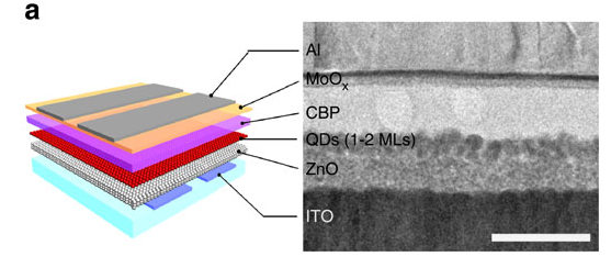
“Uma vez encontrado o material que teria o melhor efeito, foram fabricados os LEDs e pudemos confirmar os resultados esperados”, conta Padilha. A confirmação ocorreu através de uma série de medidas espectroscópicas dos pontos quânticos dentro dos dispositivos.
De acordo com Padilha, com os novos materiais desenvolvidos, os cientistas conseguiram obter LEDs de pontos quânticos até 10 vezes mais eficientes, com uma taxa de conversão de energia elétrica em energia luminosa da ordem de 8%.