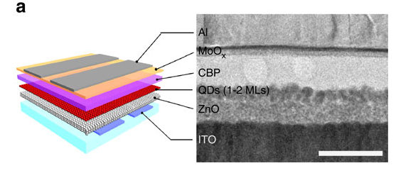
[Paper: Evidence of Band-Edge Hole Levels Inversion in Spherical CuInS2 Quantum Dots. Gabriel Nagamine, Henrique B. Nunciaroni, Hunter McDaniel, Alexander L. Efros, Carlos H. de Brito Cruz, and Lazaro A. Padilha. Nano Lett., 2018, 18 (10), pp 6353–6359. DOI: 10.1021/acs.nanolett.8b02707]
Quantum dots with unique rules
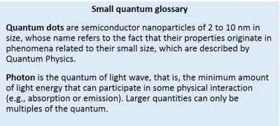 A paper led by Brazilian researchers has revealed surprising news about the rules that determine the energy levels of electrons in quantum dots of copper and indium disulphide (CuInS2,) which stand out in the family of quantum dots for being non-toxic. The work was recently reported in Nano Letters (impact factor of 12.08).
The results of the study, confirmed by experimental and theoretical methods, showed a situation in the structure of energy bands that had never before been observed in other materials.
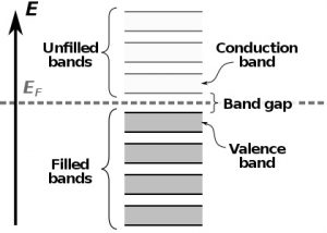
The band structure is a well-established scientific model that shows which energy states or levels the electrons can occupy in a given material. These states of energy are represented as allowed bands (those that the electrons can reach) and forbidden bands (those in which the electrons cannot be found).
In semiconductors, the energy bands that are allowed for an electron and that determine the properties of a material are the valence band and the conduction band. Both are separated by a band gap. For electrons to “jump” from the valence band to the conduction band, transposing the forbidden band in a process called transition, it is necessary they receive extra energy, which can occur when the material absorbs photons. When they lose energy, these electrons can once again occupy their places in the conduction band, and surplus energy can be emitted as photons (light). This light emission from the absorption of photons is known as photoluminescence.
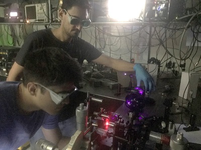
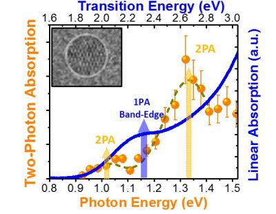
Researchers at the Gleb Wataghin Institute of Physics at UNICAMP (Campinas, SP, Brazil) discovered that the quantum dots they were studying did not follow the same transition rules as other semiconductor materials and nanomaterials. “Generally, in semiconductors, bulk or nanostructured, the states that form the top of the valence band and the bottom of the conduction band are such that a transition between these states by absorption of a photon is allowed,” contextualizes Lázaro Aurélio Padilha Junior, professor at UNICAMP and corresponding author of the article. “What we showed was that in the studied material (CuInS2 quantum dots), this transition is forbidden by absorbing one photon. The interaction with two photons is required for this transition to occur. As far as we know, this is the first semiconductor system that presents this inversion of states,” says Padilha.
The discovery, besides showing that the norms that govern the electron states in semiconductors are not valid for all the materials, can influence the applications of the quantum dots studied. According to Padilha, the conditions discovered favor the simultaneous emission of two photons in the material when the electrons return to the conduction band. “This could be attractive to lasers systems that emit light in two distinct colors at the same time, and with color adjustment over a wide spectral range,” says the professor. In addition, adds Gabriel Nagamine, the first author of the article, understanding the structure of material bands can improve the performance of existing applications such as luminescent solar concentrators – a technology that can be used both to generate electricity from sunlight and to increase the production of food in greenhouses. “All these applications come from the unique characteristics of the electronic bands of these materials,” says Nagamine.
History of a theoretically announced experimental result
The history of this discovery goes back to 2015, when Professor Padilha, who has worked with quantum dots since 2010, his master’s student Gabriel Nagamine and other members of the research group decided to devote their efforts in studying the quantum dots of CuInS2. “This material caught our attention because it did not have heavy metals in its composition, which made it interesting for applications in biology and medicine, such as fluorescent biological markers,” says Padilha. In fact, quantum dots, which were discovered in the 1980s and are now present in products such as TV screens, present very interesting properties to be used in the detection of diseases and other applications in the health area, but almost all of them are toxic due to their chemical composition.
The UNICAMP team then collaborated with the company UbiQD, located in Los Álamos (USA) and specialized in the production of quantum dots, and which provided samples of spherical and pyramidal quantum dots. The characterization of the samples was performed partly in the company and also in the National Nanotechnology Laboratory (LNNano) of CNPEM, in the city of Campinas (SP, Brazil).
Initially, Padilha and his team set out to investigate how strong the absorption of two photons was in the chosen material, since this optical process allows to make three-dimensional images of the material, which can be very useful in its characterization and also in its application in several areas. To do this, in early 2016, the team performed the main experiments of the work at UNICAMP using a spectroscopy technique that allows detecting light emission from the absorption of two photons. “The first measurements revealed an absorption peak of two photons at smaller energies than those of linear absorption – a fact never previously observed experimentally,” Padilha says. “We believed it was a problem in our laser source and we repeated the experiment, achieving the same results,” he adds. These results, which are shown in the figure to the side, have arisen from the experiments performed with spherical quantum dots. In the pyramid-shaped quantum dot samples, the predominance of of two-photon absorption was not observed.
In May of the same year Padilha met with Dr. Alexander Efros (Naval Research Laboratory, USA) at a conference in South Korea. “He, who is one of the most respected theorists working on the electronic structure of semiconductor quantum dots, mentioned that he had made calculations that predicted a reversal in parity of states in these nanomaterials. We immediately noticed that I had proven his theory, “says Prof. Padilha. After that, they began working together and trying to understand other aspects of the problem, until they submitted the article to Nano Letters. The paper was accepted in less than two months.
The research that originated the paper is part of Gabriel Nagamine’s master’s thesis, defended in 2017 at UNICAMP, and received financial support from Brazilian research agencies (FAPESP and federal CNPq), the student support service (SAE) of UNICAMP and the Office of Naval Research (USA).
