Featured article: Probing electrons of actinide compounds.

box englishA team led by researchers from Brazil was able to unveil details of the distribution of electrons in materials based on actinide elements (the 15 chemical radioactive elements, with atomic numbers ranging from 89 to 103).

The group of scientists developed an experimental method that allowed a unique probing of the 5f and 6d orbitals and their hybridization in materials based on uranium (one of the most abundant actinide elements in the earth’s crust). This allowed the team to demonstrate, for example, that 5f-6d hybridization determines the magnetic properties of the studied materials. The work left as a legacy an experimental system for research on various magnetic materials (3d metals, rare earths, actinides and others), available to be used by the international scientific community at the Brazilian Synchrotron Light Laboratory (LNLS).

The study was reported in a paper that was recently published in Nature Communications (Impact Factor 12,124). “In this paper, we demonstrate the use of magnetic circular dichroism (XMCD) on the L-border of uranium to directly probe the 6d and 5f orbitals and also their degree of hybridization, rather than just probing the 5f orbitals as for instance the actinides M absorption edges,” details the corresponding author of the paper, Narcizo Marques de Souza Neto, professor at UNICAMP and researcher at LNLS.

In order to probe the orbitals of the uranium compounds, especially UCu2Si2 and UMn2Si2, the scientists had to overcome the difficulties of manipulating the materials due to their toxicity. They also had to make a series of adjustments in the high-energy XMCD technique to improve its sensitivity (to extend its detection limits).

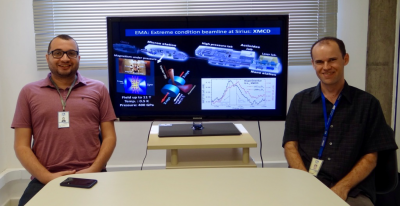
These developments were initially performed at the LNLS DXAS line, dedicated to X-ray absorption techniques. Currently, the XMCD instrumentation is part of the XDS line of LNLS which is dedicated to X-ray diffraction and spectroscopy, where it is being used and improved. In the future the technique will be available in Sirius (the latest generation of synchrotron light source which is being built in Campinas), more precisely in the EMA line, which will be dedicated to X-ray techniques under extreme conditions of pressure and temperature. According to Souza-Neto, who coordinates both the XDS line and the EMA project, the conditions for studying actinides and similar materials by XMCD will be unparalleled in Sirius.

In addition to advancing the knowledge on actinides, the research demonstrated the potential of the XMCD technique improved by the Brazilian team to continue unveiling the characteristics of these still experimentally understudied elements. A deeper understanding of actinides, says Souza-Neto, is necessary to propose new uses for these elements, and also to be able to use them more efficiently in existing applications, such as, for example, power generation, diagnosis and treatment of diseases and the production of special glasses.

Ricardo dos Reis (left) and Narcizo Souza-Neto (right), main authors of the paper. Between them, a screen with the representation of EMA beamline where XMCD experiments will be available in Sirius fourth-generation synchrotron source.

The history behind this work

The origin of this work dates back to 2009, when Souza-Neto was studying rare earth electronic structure and magnetism during his postdoctoral fellowship at the Argonne National Laboratory in the United States. “I had the idea of expanding the study of rare earths to actinide compounds (Souza-Neto et al., Phys. Rev. Lett., 102, 057206 (2009)) using XMCD to probe a charge transfer in the 4f and 5d orbitals”, the researcher reports. Looking for materials with similar characteristics, he came across uranium compounds. “We first tried to start this study in Argonne, but the conditions there to carry this out were not as we had hoped,” he adds. He returned to Brazil in 2010 as a researcher of CNPEM, with the desire to continue this initiative. Thus, in 2011, Souza-Neto began to guide the doctoral research of Ricardo Donizeth dos Reis on this subject together with the co-supervisor Flávio César Guimarães Gandra, a professor at Unicamp, with whom he had previously collaborated.

Samples of uranium compounds were prepared and characterized in the Laboratory of Metals and Alloys of Unicamp, coordinated by Professor Gandra, where there was already research experience on actinide and rare earth materials. The X-ray absorption spectroscopy experiments were performed at Argonne’s Advanced Photon Source and at LNLS. “All experiments on the L edges of uranium, which make up the main innovative contribution of this work, were carried out at LNLS,” Souza-Neto details. “At Argonne the experiments were carried out on the M edge of uranium to probe the contribution of the 5f orbitals separately and corroborate our interpretation of the results,” he adds. Furthermore, the Brazilian group had the participation of a researcher from France in the theoretical simulations performed for interpreting the data.

The research was carried out with financial resources from the São Paulo Research Foundation; from the Brazilian federal agency Capes; from the Ministry of Science, Technology and Innovation of Brazil, and from the Office of Science of the United States Department of Energy.

Scientific paper:

“Unraveling 5f-6dhybridization in uraniumcompounds via spin-resolved L-edge spectroscopy”. R. D. dos Reis, L. S. I. Veiga, C. A. Escanhoela Jr., J. C. Lang, Y. Joly, F. G. Gandra, D. Haskel & N. M. Souza-Neto. Nature Communications 8:1203 (2017). DOI: 10.1038/s41467-017-01524-1. Link: https://www.nature.com/articles/s41467-017-01524-1

Featured paper: Towards two-dimensional diamond.

Two-dimensional materials, those whose thickness goes from an atom to a few nanometers, have unique properties related to their dimensionality and are protagonists in the development of nanotechnology and nanoengineering.

A team of scientists from five Brazilian institutions and one American institution took an important step in the development of the two-dimensional diamond version. This work on 2D diamond was reported in a paper published in Nature Communications (impact factor 12,124) with open access.

“Our work presented spectroscopic evidence of the formation of a two-dimensional diamond, which we named diamondene”, says Luiz Gustavo de Oliveira Lopes Cançado, professor at the Brazilian Federal University of Minas Gerais (UFMG) and corresponding author of the paper. In choosing the name of the new material, the scientists followed the tradition of using the suffix “ene” for two-dimensional materials, as with graphene, 2D version of the graphite.

box_enIn fact, it was from the compression of graphene sheets that the diamondene was obtained by the team led by Professor Cançado. Initially, the team deposited two layers of graphene one on top of the other and transferred the graphene bilayer to a Teflon substrate, chosen for being chemically inert, preventing the formation of bonds with the graphene.

The sample of bi-layered graphene on Teflon was then subjected to high pressures and simultaneously analyzed by Raman spectroscopy at the Laboratory of Vibrational Spectroscopy and High Pressure of the Department of Physics of the Brazilian Federal University of Ceará (UFC). The experimental system used was a diamond anvil cell with a coupled Raman spectrometer. This equipment allows high pressure to be applied to small samples that are immersed in a pressure transmitting medium (in this case, water). The pressure is applied through two pieces of diamond (material chosen for being one of the hardest and resistant to compression), which compress the transmitting medium, which passes the pressure to the sample. At the same time, the spectrometer allows to monitor the changes that occur in the structure of the sample material against the different pressures applied. “In Raman spectroscopy, light behaves like a probe that measures vibrational states of the material,” explains Cançado. As a result of the probing, the spectrometer generates graphs (spectra), through which it is possible to identify the structure of the material being studied.

By analyzing the spectra, the team of scientists observed changes in the two-dimensional material that indicated the transition from a graphene structure to a diamond structure. The researchers were able to conclude that the diamondene was obtained at a pressure of 7 gigapascals (GPa), tens of thousands of times higher than the atmospheric pressure. “The evidence we present in this work is a signature in the vibrational spectrum obtained from a two-dimensional carbon material that indicates the presence of sp3 bonds, typical of the structure of the diamond,” says Professor Cançado.

To explain the formation of diamondene, the team used first principles calculations following the Density Functional Theory and Molecular Dynamics simulations. “These theoretical results guided the experiments and allowed us understanding the experimental results,” says Cançado.

Scheme of the diamondene formation mechanism from two layers of graphene submitted to high pressures (blue arrows) in water as pressure transmitting medium. The gray colored balls represent the carbon atoms; the red ones, the oxygen atoms, and the blue ones, the hydrogen atoms.

According to the theoretical results, when the bilayer graphene system on inert substrate with water as pressure transmitting medium is subjected to high pressures, the distances between the elements of the system decrease and new connections occur among them. “When applying this level of pressure on graphene, connections can change, going from the sp2 configuration to the sp3 configuration,” explains Professor Cançado. The carbon atoms in the upper graphene layer then establish covalent bonds with four neighboring atoms: the atoms of the lower layer and the chemical groups offered by water (OH- and H). The latter are fundamental to stabilize the structure. In the lower layer, in contact with the inert substrate, half of the carbon atoms are bound to only three neighboring atoms. “The pending connections give rise to a gap opening in the electronic structure, as well as polarized spin bands,” adds Cançado.

This feature makes diamondene a promising material for the development of spintronics (the emerging strain of electronics at the nanoscale in spin-bases electronics). According to Cançado, diamondene could also be used in quantum computing, microelectromechanical systems (MEMS), superconductivity, electrodes for electrochemistry-related technologies, DNA engineering substrates and biosensors – applications in which thin diamond films have already proven to have good performance.

However, there is still a long way to go before demonstrating the diamondene applications. Firstly, because the diamondene shown in the article dismantles under normal pressure conditions. To overcome this limitation, the group of Professor Cançado at UFMG is setting up an experimental system that will allow the application of much higher pressures to the samples in the order of 50 GPa and analyze them using Raman spectroscopy. “With this we intend to produce stable diamondene samples, which remain in this form even after having the pressure reduced to the level of ambient pressure,” says Cançado.

In addition, since Raman spectroscopy provides indirect evidence of the structure of the material, it will be necessary to perform direct measurements of the diamondene to know its structure in detail. “The most promising techniques in this case would be X-ray diffraction in synchrotron light sources or electron diffraction,” suggests Cançado. “The complicating factor in this experiment is the need to have the sample subjected to high pressures,” he adds.

The Brazilian history of diamondene

The idea of the 2D diamond formation originated in the doctoral research of Ana Paula Barboza, conducted under the guidance of Professor Bernardo Ruegger Almeida Neves and defended in 2012 in the Department of Physics of UFMG. In this work, Cançado says, atomic force microscopy (AFM) tips were used to apply high pressures on one, two and several layers of graphene. Indirect evidence of the formation of a two-dimensional diamond was obtained by means of electric force microscopy (EFM). The work showed the importance of the presence of two layers of graphene and water for the formation of the sp3 two-dimensional structure. The main results of the research were reported in the article Room-temperature compression induced diamondization of a few-layer graphene [Advanced Materials 23, 3014-3017 (2011)].

Main article authors. On the left, Luiz Gustavo Pimenta Martins (MSc from UFMG and doctoral student at MIT). On the right, Professor Luiz Gustavo Cançado (UFMG).

“The idea of measuring the Raman spectrum of graphene under high pressure conditions (using anvil diamond cells) came after Luiz Gustavo Pimenta Martins, an undergraduate student at the time, developed a very efficient method of transferring graphene to different substrates,” says Professor Cançado. This development was carried out during a visit to the laboratory of Professor Jing Kong at the Massachusetts Institute of Technology (MIT), after having won a grant for international mobility of the Formula Santander Award. During his master’s degree at the Physics Department of UFMG, carried out under the guidance of Professor Cançado and defended in 2015, Pimenta Martins carried out an extensive and systematic work to obtain Raman spectra of graphene samples subjected to high pressures. “There were many visits to UFC and much study until understanding the diamondene formation mechanisms,” explains Cançado.

The research reported in the Nature Communications paper was made possible by the collaborative work of several Brazilian research groups with recognized expertise in various subjects, as well as the participation of the MIT researcher in the sample preparations. Scientists from the physics departments of UFMG and UFC have contributed their recognized expertise in Raman spectroscopy applied to carbon nanomaterials and, in the case of UFC, in experiments under high pressure. Also participating in these experiments were researchers from the Brazilian Federal Institute of Education, Science and Technology of Ceará and the Brazilian Federal University of Piauí (UFPI). In addition, theoretical physicists from the Brazilian Federal University of Ouro Preto (UFOP) and UFMG performed calculations and computational simulations.

The research was funded by Brazilian federal agency CNPq, state agencies FAPEMIG and FUNCAP, Formula Santander Program and UFOP.

[Paper: Raman evidence for pressure-induced formation of diamondene. Luiz Gustavo Pimenta Martins, Matheus J. S. Matos, Alexandre R. Paschoal, Paulo T. C. Freire, Nadia F. Andrade, Acrísio L. Aguiar, Jing Kong, Bernardo R. A. Neves, Alan B. de Oliveira, Mário S.C. Mazzoni, Antonio G. Souza Filho, Luiz Gustavo Cançado. Nature Communications 8, Article number: 96 (2017). DOI:10.1038/s41467-017-00149-8. Disponível em: https://www.nature.com/articles/s41467-017-00149-8]

Artigo em destaque: Pontos quânticos desenvolvidos para LEDs mais eficientes.

O artigo científico de membros da comunidade brasileira de pesquisa em Materiais em destaque neste mês é:

Wan Ki Bae, Young-Shin Park, Jaehoon Lim, Donggu Lee, Lazaro A. Padilha, Hunter McDaniel, Istvan Robel, Changhee Lee, Jeffrey M. Pietryga & Victor I. Klimov. Controlling the influence of Auger recombination on the performance of quantum-dot light-emitting diodes. Nature Communications 4, article number 2661, published 25 October 2013. doi:10.1038/ncomms3661.

Texto de divulgação: 

Pontos quânticos desenvolvidos para LEDs mais eficientes

Um trabalho de pesquisa publicado no mês de outubro na Nature Communications, revista científica de conteúdo aberto do grupo Nature, resultou num material que aumenta dezenas de vezes a eficiência de LEDs de pontos quânticos ao diminuir a influência do efeito Auger, um dos principais limitadores da eficiência desses dispositivos que apresentam grande potencial para serem usados em iluminação, entre outras aplicações. O trabalho foi realizado no Grupo de Nanotecnologia e Espectroscopia Avançada do Laboratório Nacional de Los Alamos, localizado no sul dos Estados Unidos, com a participação de um doutor brasileiro, Lázaro Padilha, e com a colaboração de grupos da Coreia.

“O resultado veio depois de mais de um ano de pesquisa sobre como efetivamente minimizar o efeito Auger em pontos quânticos”, relata Padilha, atualmente professor do Instituto de Física da Unicamp, que chegou a Los Alamos em 2010 para fazer um estágio de pós-doutorado. O trabalho que gerou o paper na Nature Communications, além de outros artigos em periódicos de alto fator de impacto como Nano Letters e ACS Nano, começou no final de 2011 e, na sua primeira etapa, visou entender o processo físico para minimizar a influência do chamado “efeito Auger” ou “recombinação Auger” nos pontos quânticos.

Os pontos quânticos, cristais semicondutores de alguns nanometros de tamanho, apresentam propriedades que possibilitam a emissão de luz com brilho intenso e cores puras e podem ser fabricados usando técnicas simples e de baixo custo. Por esses motivos, essas nanopartículas são materiais interessantes para a fabricação de LEDs. Desde a primeira demonstração de LEDs de pontos quânticos, ocorrida em 1994 (Nature 370, 354 – 357, 04 August 1994; doi:10.1038/370354a0), esses dispositivos têm sido objeto de pesquisas visando otimizar sua capacidade de converter eletricidade em luz.

Nos LEDs, a emissão de luz se produz quando, ao se introduzir energia no dispositivo por meio de corrente elétrica, ocorrem recombinações nos átomos do material emissor. Especificamente, elétrons próximos ao núcleo do átomo saem de seu lugar deixando vagas, as quais são preenchidas por elétrons mais distantes, dotados de mais energia. A energia excedente pode sair em forma de fóton, ocorrendo a desejada emissão de luz, ou pode ser transmitida a um terceiro elétron, que será ejetado do átomo. Esta segunda possibilidade constitui o efeito Auger, que pode ser visto como um concorrente da emissão de luz no uso da energia.

Nanoengenharia dos pontos quânticos

Depois de compreender como minimizar a recombinação Auger nos pontos quânticos do ponto de vista físico e constatar que impacta significativamente na eficiência dos LEDs, o grupo de Los Alamos se propôs a desenvolver o material que teria o melhor desempenho frente a esse efeito. “Eu trabalhei nos estudos de espectroscopia para entender os processos físicos que levariam a um melhor desempenho dos materiais como base para LEDs”, diz Lázaro Padilha.

O desenvolvimento do material foi feito a partir de pontos quânticos compostos por um núcleo de seleneto de cádmio (CdSe) e uma casca de sulfeto de cádmio (CdS). Para conseguir a redução da influência do efeito Auger, os cientistas aplicaram duas estratégias de nanoengenharia: a variação da espessura da casca e a introdução de uma camada composta por uma liga de zinco, cádmio e enxofre (ZnCdS) entre o núcleo e a casca.

Após concluir, em Los Alamos, o desenvolvimento do material base, os colaboradores da Coreia do construíram LEDs com uma arquitetura na qual a camada emissora, formada pelos pontos quânticos, ficou inserida entre as camadas de transporte de cargas negativas e positivas, sendo uma inorgânica e a outra orgânica, respectivamente, como mostra a figura a seguir, extraída do artigo da Nature Communications:


“Uma vez encontrado o material que teria o melhor efeito, foram fabricados os LEDs e pudemos confirmar os resultados esperados”, conta Padilha. A confirmação ocorreu através de uma série de medidas espectroscópicas dos pontos quânticos dentro dos dispositivos.

De acordo com Padilha, com os novos materiais desenvolvidos, os cientistas conseguiram obter LEDs de pontos quânticos até 10 vezes mais eficientes, com uma taxa de conversão de energia elétrica em energia luminosa da ordem de 8%.