Featured paper: Aluminum flakes to produce carbon nanotubes.

[Paper: High-yield synthesis of bundles of double- and triple-walled carbono nanotubes on aluminum flakesThiago H.R. da Cunha, Sergio de Oliveira, Icaro L. Martins, Viviany Geraldo, Douglas Miquita, Sergio L.M. Ramos, Rodrigo G. Lacerda, Luiz O. Ladeira, Andre S. Ferlauto. Carbon 133(2018) 53-61.]

Aluminum flakes to produce carbon nanotubes

Scanning electron microscopy image of carbon nanotube bundles obtained by the method of the CTNano team.

A team of scientists from institutions in Minas Gerais made a promising contribution to the production of carbon nanotubes. These hollow cylinders, whose carbon walls are only 1 atom thick, are already part of some products (batteries, automotive materials, water filters), but their industrial production is still incipient and needs solutions to lower costs and to increase efficiency, among other challenges.

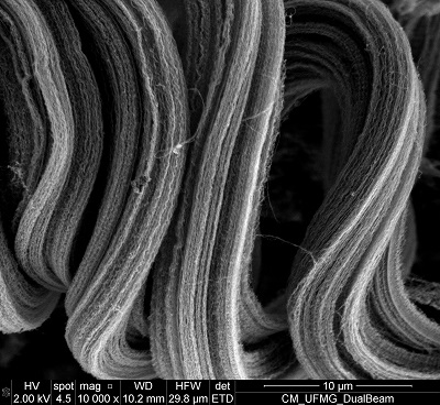
The Brazilian researchers introduced a novelty in a stage of one of the most consolidated techniques for the mass production of nanotubes, chemical vapor deposition (CVD). As a result, the team was able to produce double- and triple-walled nanotube bundles (somewhat similar to two or three hollow cylinders, one inside the other). Thin, long and of high purity, the nanotubes had diameters of 3 to 8 nanometers, lengths up to 50 thousand times the diameter (from 150 to 300 micrometers) and 90% of carbon in their composition.

“The main contribution of this work is the presentation of a scalable and cost effective process for the synthesis of carbon nanotube bundles with large surface area (625 m2/g) and aspect ratio (50000:1),” says Thiago Henrique Rodrigues da Cunha, researcher of the Nanomaterials Technology Center (CTNano) of the Brazilian Federal University of Minas Gerais (UFGM) and corresponding author of this paper, which was recently published in the journal Carbon (impact factor 2017 = 7,082).

The method, in addition to generating good quality nanotubes, allows producing relatively large quantities of this material using relatively low amounts of raw materials. “Even using small systems, it is possible to obtain carbon nanotubes at a kilogram/day scale,” says the researcher. As the nanotubes obtained showed a very large ratio between surface area and mass (more than 625 square meters weighing only one gram), the production of nanotubes by this method could reach a few million square meters per day.

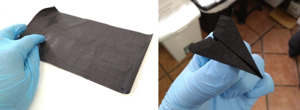
With the nanotubes obtained and a type of alcohol, the scientific team prepared a paste which was distributed over filter paper, forming a film that was separated from the paper when the paste dried. The black film was 40 micrometers thick and was flexible and foldable. Macroscopic aggregates of carbon nanotubes like this are commonly called buckypapers.

On the left, carbon nanotube film (buckypaper) produced by the team. On the right, an airplane made with this buckypaper.

“The buckypaper produced from these nanotubes exhibited great surface area and good electrical conductivity, which makes them particularly interesting in the manufacture of electrodes for batteries and supercapacitors,” says Thiago da Cunha, who adds that the CTNano team is already working to use the buckypapers in these energy storage devices. A patent on the process was deposited at the end of 2017. “Our intention is to introduce this technology to potential partners in order to convert it into a high value-added product,” reveals Cunha.

The secret of the process

Scanning electron microscopy image of carbon nanotube bundles that grew from both sides of an aluminum flake.

The CVD nanotube production processes take place inside a tube furnace into which gas containing carbon and catalytic nanoparticles are inserted. Subjected to high temperatures, the gas decomposes, and the carbon atoms deposit on top and around the nanoparticles, forming tubes (the nanotubes). The nanoparticles can be prepared in the same furnace used for nanotube growth.

The secret of the method developed by the Minas Gerais team lies precisely in the preparation of the catalytic nanoparticles. In broad lines, it is a matter of preparing a powder containing iron (Fe) and cobalt (Co) on aluminum flakes (material that had never before been mentioned in the scientific literature as a support for the growth of nanoparticles). The mixture is then subjected to temperatures of 350 to 650 °C for 4 hours, in an atmosphere similar to the air we breathe. This process, known as calcination, produces nanoparticles of iron and/or cobalt oxides. Then, the catalyst nanoparticles, still on the aluminum flakes, are introduced into the CVD furnace, whose internal temperature is brought to 730 °C. The ethylene gas (C2H4) is then introduced, which supplies the carbon so that the nanotubes grow perpendicular to the aluminum flakes.

Scientists observed an interesting advantage of using this new medium. During the calcination, a thin layer of aluminum oxide is formed on the surface of the aluminum that encapsulates the nanoparticles and prevents them from agglomerating or spreading. In addition, in the next step of the process, the aluminum oxide acts as a matrix of the nanotubes, driving their growth in the form of aligned bundles.

To test whether the calcination temperature of the nanoparticles would influence their performance as catalysts, the CTNano team carried out some experiments. The conclusion was that calcination at temperatures of 500-550 °C produces more mixed oxide nanoparticles (containing both iron and cobalt, of the CoFe2O4 formula) and produces better results in the production of nanotubes, both quantitatively (yield) and qualitative (diameter of the nanotubes).

“Unlike other methods described in the literature, which generally display low yield and are dependent on relatively expensive techniques (evaporation, sputtering) for the preparation of the catalyst, we describe in this paper a simple method to produce a catalyst in powder form, which can be used for continuous production of few-walled nanotubes using the chemical vapor deposition technique (CVD),” summarizes Thiago da Cunha.

CTNnano

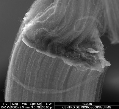
The work was funded by the Brazilian agencies Fapemig (Minas Gerais State Research Foundation) and CNPq, as well as Petrobras. The work was carried out at CTNano, except for the microscopy images, conducted at the UFMG Microscopy Center.

CTNano emerged in 2010 based on the motivation to develop products, processes and services using carbon nanotubes and graphene, in order to meet industrial demands in line with the training of qualified human resources. The research realized in CTNano has already originated 26 patents and contributed to the development of more than 200 researchers in the area. According to Thiago da Cunha, CTNano will inaugurate, in 2018, its own headquarters with an area of approximately 3,000 m², located in the Technology Park of Belo Horizonte (BH-TEC).

Authors of the paper, from UFMG, except for Viviany Geraldo, who is a professor at the Federal University of Itajubá (UNIFEI).


Featured paper: Towards two-dimensional diamond.

Two-dimensional materials, those whose thickness goes from an atom to a few nanometers, have unique properties related to their dimensionality and are protagonists in the development of nanotechnology and nanoengineering.

A team of scientists from five Brazilian institutions and one American institution took an important step in the development of the two-dimensional diamond version. This work on 2D diamond was reported in a paper published in Nature Communications (impact factor 12,124) with open access.

“Our work presented spectroscopic evidence of the formation of a two-dimensional diamond, which we named diamondene”, says Luiz Gustavo de Oliveira Lopes Cançado, professor at the Brazilian Federal University of Minas Gerais (UFMG) and corresponding author of the paper. In choosing the name of the new material, the scientists followed the tradition of using the suffix “ene” for two-dimensional materials, as with graphene, 2D version of the graphite.

box_enIn fact, it was from the compression of graphene sheets that the diamondene was obtained by the team led by Professor Cançado. Initially, the team deposited two layers of graphene one on top of the other and transferred the graphene bilayer to a Teflon substrate, chosen for being chemically inert, preventing the formation of bonds with the graphene.

The sample of bi-layered graphene on Teflon was then subjected to high pressures and simultaneously analyzed by Raman spectroscopy at the Laboratory of Vibrational Spectroscopy and High Pressure of the Department of Physics of the Brazilian Federal University of Ceará (UFC). The experimental system used was a diamond anvil cell with a coupled Raman spectrometer. This equipment allows high pressure to be applied to small samples that are immersed in a pressure transmitting medium (in this case, water). The pressure is applied through two pieces of diamond (material chosen for being one of the hardest and resistant to compression), which compress the transmitting medium, which passes the pressure to the sample. At the same time, the spectrometer allows to monitor the changes that occur in the structure of the sample material against the different pressures applied. “In Raman spectroscopy, light behaves like a probe that measures vibrational states of the material,” explains Cançado. As a result of the probing, the spectrometer generates graphs (spectra), through which it is possible to identify the structure of the material being studied.

By analyzing the spectra, the team of scientists observed changes in the two-dimensional material that indicated the transition from a graphene structure to a diamond structure. The researchers were able to conclude that the diamondene was obtained at a pressure of 7 gigapascals (GPa), tens of thousands of times higher than the atmospheric pressure. “The evidence we present in this work is a signature in the vibrational spectrum obtained from a two-dimensional carbon material that indicates the presence of sp3 bonds, typical of the structure of the diamond,” says Professor Cançado.

To explain the formation of diamondene, the team used first principles calculations following the Density Functional Theory and Molecular Dynamics simulations. “These theoretical results guided the experiments and allowed us understanding the experimental results,” says Cançado.

Scheme of the diamondene formation mechanism from two layers of graphene submitted to high pressures (blue arrows) in water as pressure transmitting medium. The gray colored balls represent the carbon atoms; the red ones, the oxygen atoms, and the blue ones, the hydrogen atoms.

According to the theoretical results, when the bilayer graphene system on inert substrate with water as pressure transmitting medium is subjected to high pressures, the distances between the elements of the system decrease and new connections occur among them. “When applying this level of pressure on graphene, connections can change, going from the sp2 configuration to the sp3 configuration,” explains Professor Cançado. The carbon atoms in the upper graphene layer then establish covalent bonds with four neighboring atoms: the atoms of the lower layer and the chemical groups offered by water (OH- and H). The latter are fundamental to stabilize the structure. In the lower layer, in contact with the inert substrate, half of the carbon atoms are bound to only three neighboring atoms. “The pending connections give rise to a gap opening in the electronic structure, as well as polarized spin bands,” adds Cançado.

This feature makes diamondene a promising material for the development of spintronics (the emerging strain of electronics at the nanoscale in spin-bases electronics). According to Cançado, diamondene could also be used in quantum computing, microelectromechanical systems (MEMS), superconductivity, electrodes for electrochemistry-related technologies, DNA engineering substrates and biosensors – applications in which thin diamond films have already proven to have good performance.

However, there is still a long way to go before demonstrating the diamondene applications. Firstly, because the diamondene shown in the article dismantles under normal pressure conditions. To overcome this limitation, the group of Professor Cançado at UFMG is setting up an experimental system that will allow the application of much higher pressures to the samples in the order of 50 GPa and analyze them using Raman spectroscopy. “With this we intend to produce stable diamondene samples, which remain in this form even after having the pressure reduced to the level of ambient pressure,” says Cançado.

In addition, since Raman spectroscopy provides indirect evidence of the structure of the material, it will be necessary to perform direct measurements of the diamondene to know its structure in detail. “The most promising techniques in this case would be X-ray diffraction in synchrotron light sources or electron diffraction,” suggests Cançado. “The complicating factor in this experiment is the need to have the sample subjected to high pressures,” he adds.

The Brazilian history of diamondene

The idea of the 2D diamond formation originated in the doctoral research of Ana Paula Barboza, conducted under the guidance of Professor Bernardo Ruegger Almeida Neves and defended in 2012 in the Department of Physics of UFMG. In this work, Cançado says, atomic force microscopy (AFM) tips were used to apply high pressures on one, two and several layers of graphene. Indirect evidence of the formation of a two-dimensional diamond was obtained by means of electric force microscopy (EFM). The work showed the importance of the presence of two layers of graphene and water for the formation of the sp3 two-dimensional structure. The main results of the research were reported in the article Room-temperature compression induced diamondization of a few-layer graphene [Advanced Materials 23, 3014-3017 (2011)].

Main article authors. On the left, Luiz Gustavo Pimenta Martins (MSc from UFMG and doctoral student at MIT). On the right, Professor Luiz Gustavo Cançado (UFMG).

“The idea of measuring the Raman spectrum of graphene under high pressure conditions (using anvil diamond cells) came after Luiz Gustavo Pimenta Martins, an undergraduate student at the time, developed a very efficient method of transferring graphene to different substrates,” says Professor Cançado. This development was carried out during a visit to the laboratory of Professor Jing Kong at the Massachusetts Institute of Technology (MIT), after having won a grant for international mobility of the Formula Santander Award. During his master’s degree at the Physics Department of UFMG, carried out under the guidance of Professor Cançado and defended in 2015, Pimenta Martins carried out an extensive and systematic work to obtain Raman spectra of graphene samples subjected to high pressures. “There were many visits to UFC and much study until understanding the diamondene formation mechanisms,” explains Cançado.

The research reported in the Nature Communications paper was made possible by the collaborative work of several Brazilian research groups with recognized expertise in various subjects, as well as the participation of the MIT researcher in the sample preparations. Scientists from the physics departments of UFMG and UFC have contributed their recognized expertise in Raman spectroscopy applied to carbon nanomaterials and, in the case of UFC, in experiments under high pressure. Also participating in these experiments were researchers from the Brazilian Federal Institute of Education, Science and Technology of Ceará and the Brazilian Federal University of Piauí (UFPI). In addition, theoretical physicists from the Brazilian Federal University of Ouro Preto (UFOP) and UFMG performed calculations and computational simulations.

The research was funded by Brazilian federal agency CNPq, state agencies FAPEMIG and FUNCAP, Formula Santander Program and UFOP.

[Paper: Raman evidence for pressure-induced formation of diamondene. Luiz Gustavo Pimenta Martins, Matheus J. S. Matos, Alexandre R. Paschoal, Paulo T. C. Freire, Nadia F. Andrade, Acrísio L. Aguiar, Jing Kong, Bernardo R. A. Neves, Alan B. de Oliveira, Mário S.C. Mazzoni, Antonio G. Souza Filho, Luiz Gustavo Cançado. Nature Communications 8, Article number: 96 (2017). DOI:10.1038/s41467-017-00149-8. Disponível em: https://www.nature.com/articles/s41467-017-00149-8]

B-MRS at the annual meeting of the Brazilian Society for the Advancement of Science (SBPC).

From the left, Marcos Pimenta, Glaura Goulart Silva (scientific director of SBPMat) and Aldo Zarbin in the panel on carbon nanostructures at the 60th Annual SBPC Meeting.

The Brazilian Materials Research Society (B-MRS) was present at the 69th Annual Meeting of the SBPC  (Brazilian Society for the Advancement of Science), represented by one of its board members, Professor Glaura Goulart Silva (UFMG). A free event and open to society, the annual SBPC meeting has been held since 1948 in public universities in different Brazilian states. This year, the meeting was held at the Federal University of Minas Gerais (UFMG), in Belo Horizonte (state of Minas Gerais), from July 16 to 22, with the central theme “Innovation –Diversity – Transformations.”

“The 69th Annual SBPC Meeting was an area of resistance to the dismantling of science and technology in Brazil,” declared B-MRS scientific director, Goulart Silva. “The Brazilian community actively involved in science, of all ages, origins and functions, has united in a clear message: science and education are investments, it is on this basis that we can build a future for our people,” she said.

As part of the event’s program, Professor Goulart Silva participated in the roundtable “Carbon Nanostructures: The Next Technological Revolution?” which took place on July 17 from 3:30 p.m. to 6 p.m. The other members of the roundtable were Professor Aldo Zarbin (UFPR), President of the Brazilian Society of Chemistry (SBQ), and Professor Marcos Pimenta (UFMG), coordinator of the INCT of Carbon Nanomaterials and of the Center for Nanomaterials (CTNano), of which Professor Goulart Silva is vice-coordinator.

Carbon nanomaterials, their structure, properties and applications were presented at the roundtable, which had a large audience and many questions raised, focusing on their potential to contribute to various technological areas. “We discussed how nanotechnology can impact a new technological era that has sustainability as a fundamental requirement,” informed the scientific director of SBPMat. “The members and participants of the roundtable expounded on a joint vision that a wide range of nanomaterials will occupy relevant spaces in future technologies. Not only carbon nanomaterials, but also that carbon nanotubes and graphene are indisputably very important systems in this set,” she says.

According to Goulart Silva, all participants in the session emphasized the need for investments in science and technology in Brazil, so that the advances made in areas such as nanotechnology continue.

Featured paper: Advanced material for ultra-capacity supercapacitors.

[Paper: One-step electrodeposited 3D-ternary composite of zirconia nanoparticles, rGO and polypyrrole with enhanced supercapacitor performance. Alves, Ana Paula P.; Koizumi, Ryota; Samanta, Atanu; Machado, Leonardo D.; Singh, Abhisek K.; Galvao, Douglas S.; Silva, Glaura G.; Tiwary, Chandra S.; Ajayan, Pulickel M. NANO ENERGY, volume 31, January 2017, 225–232. DOI: 10.1016/j.nanoen.2016.11.018.]

Advanced material for ultra-capacity supercapacitors.

Supercapacitors are electrical storage devices with a particular feature of releasing large amounts of energy in a short time interval. They are already used, for example, in electric or hybrid vehicles, camera flashes and elevators, but they can still be improved – largely with the contribution of Materials Science and Technology – for current and potential applications. Putting it simply, a supercapacitor consists of two electrodes, positive and negative, separated by a substance containing positive and negative ions (the electrolyte).

An article recently published in the scientific journal Nano Energy (Impact Factor 11,553) reports on a contribution from an international and interdisciplinary scientific team to develop materials that improve the performance of supercapacitors. Using a simple and easily scalable process, the team of researchers from Brazil, the United States and India produced electrodes made of a composite material composed of polypyrrole (PPi), reduced graphene oxide (rGO) and zirconium oxide (ZrO2) nanoparticles. By combining the three materials, the scientists were able to generate a large surface area and high porosity electrode – basic characteristics to promote the interaction of the electrolyte ions with the surface of the electrodes and therefore enhance the performance of the supercapacitor.

“Our unique contribution was the synthesis, in a single and simple stage of electrodeposition, of a hybrid containing graphene, zirconium oxide and polypyrrole, and the experimental demonstration of considerable gains in electrochemical properties, parallel to the theoretical modeling in order to understand the role of the components of the material”, states Glaura Goulart Silva, professor in the Department of Chemistry at the Federal University of Minas Gerais (UFMG) and a corresponding author of the paper.

In addition to preparing samples of the ternary (i.e., composed of three elements) composite PPi/rGO/ZrO2, using the same method for comparison purposes, the team prepared samples of the PPi/rGO binary composite, and pure polypyrrole samples. The three materials were analyzed using XPS (spectroscopy of X-ray excited photoelectrons), SEM (Scanning Electron Microscopy), Raman spectroscopy and transmission electron microscopy to determine their composition, structure and morphology.

As seen in the SEM images of the figure below, the scientists noted that the addition of graphene oxide and zirconia nanoparticles significantly changed the morphology of the material. While the pure polypyrrole had formed a cracked, wire-like film, the graphene composite had a granular morphology, with no cracks, and the zirconium oxide material had a leaf-like appearance.

At the end of the experimental stage of the study, the scientists performed a series of tests to measure the performance of the three materials as supercapacitors. The results showed that the capacity to store electrical charges (capacitance) had increased up to 100% in the ternary composite with respect to the polypyrrole. Moreover, instead of decreasing this performance due to the use of the electrode, it increased by 5% after 1,000 recharges in the binary and ternary composites.

This was the first paper that presented the introduction of zirconium oxide nanoparticles in polypyrrole and graphene electrodes for supercapacitors. Therefore, the team performed computational modeling to analyze the role of zirconium oxide in the performance of the composite. The simulations confirmed the beneficial effects of the nanoparticles on the stability of the material, directly related to extending the life of the electrodes.

Illustrative diagram of charge storage and interaction of ions near the surface of pure polypyrrole electrodes (PPi), reduced graphene oxide (PPi/rGO) and polypyrrole PPi/rGO/ZrO2 (above), based on the morphology associated with the SEM images of the surface of the electrodes with the respective materials under carbon fiber substrate (below). Image by Ana Paula Pereira Alves for her PhD thesis.
Above, illustrative diagram of charge storage and interaction of ions near the surface of pure PPi electrodes, PPi/rGO electrodes, and PPi/rGO/ZrO2 electrodes, based on the morphology associated with the SEM images of the surface of the electrodes with the respective materials under carbon fiber substrate (below). Image by Ana Paula Pereira Alves for her PhD thesis.

“There is great potential in the application of these new composites in supercapacitors due to the need to increase the energy density provided by the device, in parallel with its miniaturization,”declares Professor Goulart Silva. “The alternative developed in the work in question allows better performance in terms of cycling stability with gains in the safety of the supercapacitor. The use of supercapacitors and batteries in electric and hybrid cars is one of the technological fronts where these materials can be applied,” she adds.

From the reader's left: Professor Glaura Goulart Silva (UFMG), Professor Pulickel Ajayan (Rice University) and Ana Paula Pereira Alves, a recently graduated doctor from UFMG.
From the reader’s left: Professor Glaura Goulart Silva (UFMG), Professor Pulickel Ajayan (Rice University) and Ana Paula Pereira Alves, a recently graduated doctor from UFMG.

The work is part of the doctorate in Chemistry of Ana Paula Pereira Alves, conducted with the guidance of Professor Goulart Silva and defended in February of this year at UFMG with a thesis about synthesis and characterization of advanced materials for supercapacitors. During her doctoral work at the University of Minas Gerais, Pereira Alves carried out intensive training in synthesis techniques and physical-chemical analysis of conjugated polymers and graphene and in the characterization of supercapacitors. In 2015, she went to the United States for a one-year “sandwich” internship, with the support of the National Council for Scientific and Technological Development (CNPq), in the Department of Materials Science and Nanoengineering at Rice University, in the research group of Professor Pulickel Ajayan (researcher with h=139 index according to Google Scholar), who has collaborated with Professor Goulart Silva’s group since 2010. “Professor Ajayan has systematically proposed radical innovations in synthesis and design of batteries and supercapacitors, with significant international impact in the area,” she adds.

The experimental work reported in the paper was carried out at Rice University, with the presence of all authors, including those from Brazil and India, and also Professor Goulart Silva, who was there in February 2016, with the support of Minas Gerais Research Foundation (Fapemig). “The highly interdisciplinary environment of the Department of Materials Science and NanoEngineering at Rice made possible for the engineers, physicists, and chemists to come together to work on a current major problem.”, says Goulart Silva.

The computational modeling was carried out by Brazilian researchers from the State University of Campinas (Unicamp) and the Federal University of Rio Grande do Norte (UFRN) –among them Professor Douglas Galvão (Unicamp), who has maintained a scientific collaboration with Professor Ajayan since before the beginning of this research.

“I consider this work to be an excellent example of success, where the competence of the Brazilian groups joined that of a highly productive and impactful group in the international scenario and complement each other,” declares Goulart Silva. “The stability and increase of investments in research and development in Brazil are essential for endeavors as this to be widespread. Research is an investment that needs to be done over the long term, without setbacks, to enable a high rate of return in terms of materials, technologies and highly qualified people. Ana Paula Alves is now a young doctor in search of the opportunity to put together her research group and hence train new students and hence contribute to face the challenges of our country,” reaffirms Goulart Silva.

Featured paper: Isolating nanoribbons with conducting regions.

[Paper: Topologically Protected Metallic States Induced by a One-Dimensional Extended Defect in the Bulk of a 2D Topological Insulator. Erika N. Lima, Tome M. Schmidt, and Ricardo W. Nunes. Nano Lett., 2016, 16 (7), pp 4025–4031. DOI: 10.1021/acs.nanolett.6b00521]

Isolating nanoribbons with conducting regions

A research carried out in Brazil made an important contribution to the study of topological insulators, a class of materials that was theoretically predicted in 2005 and experimentally confirmed in 2007. The study was reported in an article recently published  in Nano Letters (impact factor: 13.779).

A unique property of Topological insulators is that they behave as insulators on the inside and as conductors on its surface or edge. According to Ricardo Wagner Nunes, professor at the Federal University of Minas Gerais (UFMG) and corresponding author of the article, “non-topological insulators may also have conductive surfaces, but in the case of topological insulators, conduction of charge and spin on the surface is robust, as it is “protected” by time reversal symmetry”.

In the article in Nano Letters, Professor Nunes and colleagues, Erika Lima, of the Federal University of Mato Grosso (UFMT) – Rondonópolis campus, and Tome Schmidt, of the Federal University of Uberlândia (UFU), reported their work on a two-dimensional topological insulator, a bismuth nanoribbon of only two layers of bismuth atoms (one-atom thick), superimposed and bonded. Using computational methods, the scientists showed that the interior of the bismuth nanoribbon, instead of being fully insulating, may have conductive states (also called metallic states) generated from a particular type of irregularity in the atomic structure of the material, known as 558 extended defect.

Representation of bismuth bilayer nanoribbon with the defect 558, top view (left) and side view (right). The green balls represent the atoms of the top layer of the material and the blue balls, the atoms of the lower layer. In the center of the left figure, the defect is clearly seen: pentagons and an octagon stop the repetition of the hexagons.


“In our work, we show that a linear defect within a two-dimensional topological insulator can generate one-dimensional electronic quantum states that conduct spin and charge within the material”, say the authors.

This conclusion was supported through calculations performed on supercomputers, simulating what would happen to the electrons in quantum states, in the material, in the presence of defects. “We used first-principles Density Functional Theory calculations”, specify the authors, who relate that the computer simulation of defects in bismuth nanostructures required approximately 400 hours of computer simulations on supercomputers in the Department of Physics – UFMG and at the National Center for High Performance Computing in São Paulo (Cenapad) – UNICAMP.

A figura mostra a curva de dispersão dos estados topológicos metálicos, localizados no defeito 558, marcados em azul e vermelho.
The figure shows, marked in blue and red, the dispersion curve of the metal topological states located in the defect 558.

In the article, the authors also propose the existence of pentaoctite, a new two-dimensional topological insulator. This material, which has not been synthesized yet, is a bismuth bilayer with a crystal lattice formed by atoms arranged in pentagons and octagons. As stated by the authors, “In our calculations we show that this new “phase” of the two-dimensional bismuth has low formation energy, which opens the possibility to be synthesized in the laboratory”.

According to the authors, the work reported in Nano Letters raises several issues in the scope of fundamental research, such as the influence of magnetic and non-magnetic impurities on the spin and charge transport in the proposed topological states, and the connection between the network symmetries and nature of the topological edge states on pentaoctite. “From the point of view of applications, it would be interesting if our work could motivate experimental studies of two-dimensional topological insulators based on bismuth and other materials, enabling theoretical and experimental collaboration on this issue”, comment the authors, leaving an open invitation to experimental research groups.

The origin of this research work

“The work originated by combining my interest in extended topological defects in two-dimensional and three-dimensional materials, with the experience of Professor Tome Mauro Schmidt (UFU) and Erika Lima, his doctoral student in the subject of topological insulators”, states Nunes.

In 2012, Nunes and collaborators published an article in Nano Letters on magnetic states (non topological) generated by linear extended defects in a monolayer of graphene. Later, in a conversation with Schmidt, a collaboration was decided in order to investigate if an extended defect with the same morphology would lead to the formation of topological states in a bidimensional topological insulator made of bismuth.

In her post-doctorate in the group of Professor Nunes, in 2015, Erika Lima performed all computer calculations. The three researchers, who are the authors of the article, interpreted the results and wrote the paper.

The research that led to the article received funding from Brazilian agencies CAPES, CNPq, FAPEMIG and from the National Institute of Science and Technology on Carbon Nanomaterials.

autores
Photos of the authors. From left to right, Erika Lima, currently a professor at UFMT, Tome Schmidt, professor at UFU, and Ricardo Nunes, professor at UFMG.

Interviews with plenary speakers of the XV B-MRS Meeting: Ado Jorio (UFMG, Brazil).

Sixteen years ago, working as a post-doctoral fellow at the Massachusetts Institute of Technology (MIT) in the group of professor Mildred Dresselhaus, the Brazilian physicist Ado Jorio de Vasconcelos headed a study that would produce the first successful result of the application of Optics, more precisely Raman spectroscopy, in the individual characterization of carbon nanotubes – keeping in mind that nanotube´s walls are just one atom thick, with diameters typically about one nanometer. In the MIT website, the page of Professor Mildred, who has been studying carbon nanostructures at MIT for more than 50 years, reinforces the importance of the work she has carried out with Jorio: 5 of the 6 publications selected by the emeritus professor are co-authored by Jorio.

When Ado Jorio began his postdoc he was 28 years old and had just finished his doctorate in Physics from the Federal University of Minas Gerais (UFMG). His thesis was on phase transitions in incommensurate systems, conducted under the guidance of Professor Marcos Assunção Pimenta. Prior to that, he earned his bachelor’s degree in Physics, also from UFMG, after studying Electrical Engineering for three years.

After the postdoc at MIT, Jorio returned to UFMG and was later accepted as associate professor of the university in 2002 via a public selection procedure. From 2007 to 2009 he held a position at the Brazilian National Institute of Metrology, Quality and Technology (Inmetro) to develop nanometrology-related activities. In 2010, he became full professor of UFMG and that same year took over the direction of the Coordination of Transfer and Innovation of the University until 2012. In 2013 he was at ETH Zurich (Switzerland) as a visiting professor, carrying out teaching and research activities. In August 2016 he became Dean for Research of UFMG.

Since 2002, Jorio has expanded the subject of his post-doctoral work. He has conducted research in optics and the development of scientific instrumentation, namely the study of carbon nanostructures with various applications. An example of this diversity is a study in which Jorio participates, in which nanotechnology field techniques are used to understand details of the composition of the “Indian black earth”, a highly fertile soil with carbon sequestration potential, which is found in places formerly inhabited by Indians in the Brazilian Amazon.

Jorio holds one of the highest H-index among scientists in Brazil: 74, according to Google Scholar. He is also one of the most cited researchers in the world, evidenced by the inclusion of his name in the latest Thomson Reuters international list, which tabulated 1% of the most frequently cited papers in each knowledge area among all the indexed scientific articles between 2003 and 2013. Jorio is the author of over 180 scientific articles and 20 books or book chapters, and 8 patent applications. According to Google Scholar, his publications combine more than 30,000 citations.

His contributions have received numerous acknowledgments from prestigious institutions, such as the Somiya Award from the International Union of Materials Research Societies in 2009; the ICTP Prize of the Abdus Salam International Centre for Theoretical Physics in 2011, and the Georg Forster Research Award by the Humboldt Foundation in 2015, among many other national and international awards.

In the XV Brazil-MRS (SBPMat) Meeting, Ado Jorio will deliver a plenary lecture on a topic in which he is one of the world’s leading experts, the use of Raman spectroscopy to study carbon nanostructures. The Brazilian scientist will talk about how the technique evolved until reaching the nanoscale. He also promises to reveal some tactics that allow using light, whose wavelength is at least hundreds of nanometers, as a probe to investigate structures of only few nanometers.

See our interview with this member of the Brazilian research community in Materials and plenary speaker at our annual event.

SBPMat Newsletter: – Tell us what led you to become a scientist and work in the Materials area.

Ado Jorio: – It was a winding path! I entered university to study electrical engineering. Back then I played in a progressive rock band, so I looked for scientific research in the area of music. I was told to talk to a teacher at the physics department who enjoyed music, studied acoustics and materials. That’s how my career began and which ended up in materials science.

SBPMat Newsletter: – In your own words, what are your main contributions to the Materials area.

Ado Jorio: – I would say there are two main contributions. The first is in the area of carbon nanotubes, I have shown that optics could be brought to the level of individual nanotubes. This gave way to a very broad research field because there are various types of nanotubes, depending on their diameter and chirality. Before this work, people were studying nanotubes. After this work, people began to study specific types of nanotubes. It would be equivalent to saying that researchers studying the atom then realized that there are different types of atoms. The article that was the linchpin of this discovery was the [PRL86, 1118 (2001)]. The second contribution was the advancement of optics to study carbon nanostructures more broadly. I worked on several fronts, from scientific instrumentation for optical measurements below the diffraction limit, to the study and characterization of defects, approaching materials of interest in soil science, biotechnology and biomedicine. Some key references are the books “Raman Spectroscopy in Graphene Related Systems” and “Bioengineering Applications of Carbon Nanostructures”.

SBPMat Newsletter: – We always invite the interviewee to leave a message for the readers who are beginning their scientific careers. Many of these readers would like to one day achieve an H index like yours. What do you say to them?

Ado Jorio: – Make a big effort to attend conferences and make great presentations, always! Science is a debate and you have to be heard. Never repeat the same presentation. Each public requires a specific focus. Of course this advice depends on funding, but since the beginning of my career I have always spent my own money to fund my travels, and I still do this.

SBPMat Newsletter: – Leave a message or invitation to your plenary lecture for the readers who will participate in the XV Brazil-MRS (SBPMat) Meeting.

Ado Jorio: – After all of the above, and since the title and abstract are available, I can only offer my thanks to those who will honor me with their presence. It will be an honor to have these colleagues in the auditorium.

————————

Link to the summary of the plenary lecture of Ado Jorio: http://sbpmat.org.br/15encontro/speakers/abstracts/7.pdf

Featured paper: Designing structures to manipulate light.

[Paper: Oxide-cladding aluminum nitride photonic crystal slab: Design and investigation of material dispersion and fabrication induced disorder. Melo, EG; Carvalho, DO; Ferlauto, AS; Alvarado, MA; Carreno, MNP; Alayo, MI. Journal of Applied Physics 119, 023107 (2016). DOI: 10.1063/1.4939773.]

Designing structures to manipulate light

Photonic crystals are nanostructures capable of manipulating visible light and other forms of electromagnetic radiation by organizing its structure in periodic patterns.

In addition to the natural materials with these characteristics, such as opal, photonic crystals are man-made and are generally classified as metamaterials. Its characteristics (shape, size and composition) are designed to control light waves. Through nanofabrication processes these become tangible structures and are used in many “nanophotonic” devices. Nevertheless, producing these structures is by no means a simple task.

The authors of the article. From left to right, at the laboratory: Prof. Marcelo Nélson Paez Carreño, Emerson Gonçalves de Melo, Maria Elisia Armas Alvarado and Prof. Marco Isaías Alayo Chávez. At the insets: Daniel Orquiza de Carvalho (left), André Santarosa Ferlauto (right).

With a study based on computer simulations, a team of Brazilian scientists headed by researchers from the Polytechnic School of the University of São Paulo (EPUSP) presented scientific contributions that can be used to improve the production of photonic crystals to enhance their performance of manipulating light. According to Emerson Melo, the first author of a paper on the study that was recently published in the prestigious Journal of Applied Physics (JAP) “the work presents a detailed analysis of the effects caused by nanofabrication processes on the optical properties of planar photonic crystals produced on silicon dioxide-cladding aluminum nitride”.

“The idea emerged from the opportunity of combining the excellent optical and physical characteristics of aluminum nitride (AlN), such as transparency over a wide wavelength range (from the near infrared to the ultraviolet range), its non-linear effects, great stability and temperature variations, with the advantages provided by photonic crystals, such as the construction of high-efficiency waveguides, curves and resonant cavities in nanoscale dimensions, in addition to the various optical effects of photonic crystals, such as very low group velocity and low-intensity nonlinear effects of the materials”, adds Emerson,  who is a doctoral student in Microelectronics – Photonics in EPUSP, within the Group of New materials and Devices of the Microelectronics Laboratory of the Department of Electronic Systems Engineering. Emerson`s doctoral research, whose advisor is Professor Marco Isaías Alayo Chávez, enquires into the study, production and characterization of nanophotonic devices such as waveguides, resonant cavities, optical modulators and switches in aluminum nitride photonic crystals.

The study that resulted in the paper published in the JAP began with an experimental stage. Thin films of aluminum nitride and silicon dioxide (SiO2) were manufactured by the EPUSP group, and with the research collaboration from UFMG and UNESP they were analyzed by the Variable Angle Spectroscopic Ellipsometry (VASE) technique to determine the dielectric functions, which was later used as the theoretical research data.

On the left, a diagram of a photonic crystal structure with some of the manufacturing defects studied. On the right, a diagram of the unit cell of the ideal photonic crystal designed by the scientists.

Then, the EPUSP group designed a photonic crystal, ideal in terms of performance and manufacturing possibilities, consisting of a layer of aluminum nitride between two silicon dioxide layers, with round holes arranged in a repeating pattern along the “sandwich” material. Using analytical and numerical methods, the USP researchers simulated some of the “side effects” of the photonic crystal manufacturing processes of this type (e.g., variations of size and location of holes) and theoretically analyzed how these imperfections affect the performance of the photonic crystal.

The theoretical research of Emerson and the other researchers of EPUSP focused on the imperfections generated in the two main stages of the nanofabrication process normally used in photonic crystals such as the one studied: electron-beam lithography and plasma-assisted dry etching. “The results presented allow to assess that the electron-beam lithography process has greater effect on the performance of devices that explore the dispersion of electromagnetic radiation through the photonic crystal, such as prisms, optical switches and modulators”, says Emerson. “However, the quality of the dry etching process has a more profound impact on the characteristics of devices into which linear or exact defects are introduced in the periodic network of the photonic crystal to insert harmonic modes within the photonic band gap. In this case, the dry etching has to be extremely well controlled for manufacturing the devices where waveguides and resonant cavities are among its main elements”.

In addition to making headway in understanding the role of nanofabrication processes of photonic crystals in the performance of nanophotonic devices, the authors of the paper were able to define a method to design planar photonic crystals with core and cover in thin film dielectric materials. “The methodology includes determining the dielectric function of the material by the spectroscopic ellipsometry technique to analyze the dispersion effects of the materials,  determining the geometrical parameters that maximize the photonic band gap and the analysis of the impacts caused by deviations introduced in the manufacturing process”, explains Emerson.

The research received financial support from the National Council for Scientific and Technological Development (CNPq) and from the Financier of Studies and Projects (Finep).

The authors of the article. From left to right, at the laboratory:.

Featured paper: Vibrations of manipulated nanotubes.

[Paper: Strain Discontinuity, Avalanche, and Memory in Carbon Nanotube Serpentine Systems. Muessnich, Lucas C. P. A. M.; Chacham, Helio; Soares, Jaqueline S.; Neto, Newton M.; Shadmi, Nitzan; Joselevich, Ernesto; Cancado, Luiz Gustavo; Jorio, Ado. Nano Lett. 2015, 15 (9), pp 5899–5904. DOI: 10.1021/acs.nanolett.5b01982]

Vibrations of manipulated nanotubes.

Scientists from Brazilian institutions, in collaboration with researchers from Israel, “manipulated” carbon nanotubes of 1 nm diameter deposited on quartz surfaces and analyzed strain and displacements produced by this nanointervention. The team identified some behavior patterns in the nanotubes – quartz system and formulated a mathematical model applicable to systems formed by one- and two-dimensional materials over various substrates. The results of the study were recently published in Nano Letters.

To perform the experiments, the Brazilian investigators used samples idealized and produced in the Weizmann Institute of Science (Israel), in which the nanotubes are serpentine-shaped (composed of parallel segments connected together by U-shaped curves).These samples offered a desirable complexity, fostered by both the nanotubes format and the anisotropic character of quartz, which makes adhesion of nanotubes to the substrate not the same at all points.

In order to “manipulate” the system, the researchers used the tip of an atomic force microscope (AFM) built in the laboratory, which allows to change the position of nanometric particles and even of atoms, and to measure in situ the optical spectrum of nanostructures. In each sample, the tip touched a point of the quartz substrate and pushed toward the nanotube, and then proceeded to the optical analysis.

Before and after nanomanipulation, the scientists analyzed a number of points in the nanotube using the technique of Raman spectroscopy, which provides information about the frequency in which the atoms vibrate in the area being studied. More specifically, researchers focused on the frequency of the “G band”, which is used to infer the strain measurements of a considered point, since changes in the frequency of the “G band” are proportional to changes in strain.

Thus, scientists were able to identify and analyze different behavior of the nanotubes after nanomanipulation; for example, the detachment of the substrate and the intense displacement of a full stretch of the nanotube that had received two manipulations at the same point.

In addition to performing the experimental work, the authors of the article in Nano Letters managed to condense the complexity of behaviors they observed in a mathematical model (an equation) capable of explaining them theoretically and predicting these phenomena in similar systems. “The paper proposes a relatively simple model to describe complex effects of nanostructures adhesion in support media,” says Ado Jório, professor in the Department of Physics of the Federal University of Minas Gerais (UFMG) signing the letter as corresponding author.

The research that led to the Nano Letters article was developed within the master’s, doctoral and postdoctoral work of three authors of the letter, in the context of the Brazilian Network for Research and Instrumentation in Optical Nano-Spectroscopy, a project funded by the National Council for Scientific and Technological Development (CNPq) and coordinated by Ado Jório. “This is the result of a broad scientific instrumentation project, which aims at reaching the level of manipulating nanostructures and measuring, accurately, the effect of this process at the nanoscale,” says Jório.

The figure shows one of the 34 serpentine-shaped nanotubes on crystalline quartz substrate studied by the authors of the article. To the left of the reader is the nanotube before manipulation. To the right, following the sequence, the same nanotube after the intervention, with the consequent evident strain. The central segment of the nanotube, where the nanomanipulation occurred, was colorized, the gray scale indicating the frequency of the G band in that place. Finally, farther to the right, the chart displays the frequency of G band measured by Raman spectroscopy in successive points of this nanotube (graphical representation of gray hues): the black circles refer to non-manipulated nanotube and the gray colored circles, to the manipulated ones.

Featured paper. Nanometric Origami: organized strain of two-dimensional materials

Paper: Crystal-oriented wrinkles with origami-type junctions in few-layer hexagonal boron nitride. Oliveira, Camilla K.; Gomes, Egleidson F. A.; Prado, Mariana C.; Alencar, Thonimar V.; Nascimento, Regiane; Malard, Leandro M.; Batista, Ronaldo J. C.; de Oliveira, Alan B.; Chacham, Helio; de Paula, Ana M.; Neves, Bernardo R. A. Nano Research. 2015, 8(5): 1680–1688. DOI: 10.1007/s12274-014-0665-y.

Camilla Oliveira at the atomic force microscope.

Camilla Oliveira was at the Federal University of Minas Gerais (UFMG), in Brazil, studying samples of hexagonal boron nitrite (hBN) with an atomic force microscope (AFM) within the framework of her doctoral studies in Physics, when one particular aspect of the control samples caught her attention and that of her advisor, Professor Bernardo Neves. After undergoing a heat treatment (annealing), the hBN had gained nanometric wrinkles, arranged in a geometric pattern that seemed to follow some sort of organization.

The researchers decided to study these wrinkles in more detail. They had an important question to answer: was there any relation between the arrangement of the wrinkles and the hBN crystal structure? In other words, did these wrinkles have a crystallographic orientation?  Until that moment, there were no records in scientific literature of crystallographically-oriented wrinkles in two-dimensional materials, but this property could be useful.

The two-dimensional hBN crystal lattice (1 atom high).

Camilla and her advisor joined other scientists from UFMG and the neighbor Federal University of Ouro Preto (UFOP) in order to carry out that research. The team produced samples composed of a few layers of hBN anchored on a silicon substrate, they heated them at 1,000 degrees Celsius and then cooled them. During this process, the silicon and the boron nitride displayed opposite strain behaviors. Due to the heating, the hBN contracts itself, while the silicon expands, shrinking the hBN. On the other hand, the cooling expands the hBN and shrinks the silicon, folding the boron nitride as origami paper.

After much experimental work using several techniques and approaches, and various simulations, the scientists were able to confirm that the wrinkles were forming in well-defined directions inside the crystal lattice. Analyzing the folding pattern in details, the scientists noticed the triangular-shaped joints by which the wrinkles (usually three of them) met.

AFM images of a 10nm thick hBN flake after the heat treatment, displaying a crystallographically-oriented pattern of wrinkles (left); details of a typical joint (right). The average height of the wrinkles is 10nm.

Detail: as proven by the Brazilian scientists, for the crystallographically-oriented folding patterns to be formed, the heat treatment must consist of rapid heating, followed by slow cooling (for example, citing the rates used in the research, 50 °C per minute to heat, and 8 °C per minute to cool). The wrinkles produced with faster cooling rates are arranged in a disorderly manner, with no crystallographic orientation.

The researchers have also concluded that this type of organized strain could happen, not only to hBN, but to other two-dimensional materials as well, such as graphene, and that it could lead to interesting applications in straintronics – the field of knowledge that studies and explores the capacity of some materials to have their properties deeply changed due to strain processes.

The results of the research were recently published on the scientific journal Nano Research.

“In my opinion, the main contribution of the paper is to present a property that may be shared by many two-dimensional materials: the organized strain, i.e., strain in well-defined crystallographic directions, of a material at the nanoscale”, says Professor Neves, who is the corresponding author of the paper.

The research was funded by the Brazilian agencies Capes, CNPq and Fapemig, and by INCT-Nanocarbono.