|
||||||||||||||||||||||||||||||||||
To unsubscribe, click here
|
||||||||||||||||||||||||||||||||||

In the 2016 edition, the Kavli Prize – nanoscience was awarded to the three scientists who invented the atomic force microscope (AFM): Gerd Binnig (IBM Zurich Research Laboratory, Switzerland), Christoph Gerber (University of Basel, Switzerland) and Calvin Quate (Stanford University, USA). The Kavli Prize has been awarded since 2008 in the fields of Astrophysics, Nanoscience and Neuroscience by the Kavli Foundation, the Norwegian Academy of Science and Letters and the Norwegian Ministry of Education and Research.
The atomic force microscope (AFM), created in the mid-1980s, was the first instrument that made possible viewing details of different kinds of materials with a resolution of less than a nanometer (on the order of angstroms). More recently, this instrument has also been used to manipulate surfaces with atomic precision, in which atoms can be pushed, pulled or slid on a surface, one by one, with the tip of the microscope.

According to the Kavli Prize website, the history of the atomic force microscope goes back to 1981 when the German physicist Gerd Binnig, along with Heinrich Rohrer and collaborators invented the scanning tunneling microscope (STM) in the IBM labs in Zürich (Switzerland). That was the first instrument that showed the composition of materials on the nanoscale, with a resolution of a few nanometers. The STM, however, had a serious limitation: it could only be used to image conductive materials. So Binnig thought about the changes he could make on the microscope that would overcome this obstacle.
In 1985 he filed the patent application of the AFM, which could produce images of samples of all kinds. He then summoned two scientists he had worked with in the development of the STM (Gerber and Quate). Together they set up the first AFM and conducted the first experiments, whose results were published in the journal Physical Review Letters in March 1986.

After three decades developing the technique and the instrument, the atomic force microscopy has now several new modes to use it, new spin-off instruments and new fields of application (including the Life Sciences).
More information on the AFM and its inventors is available in the Kavli Prize website: http://www.kavliprize.org/prizes-and-laureates/prizes/2016-kavli-prize-nanoscience
Paper: Crystal-oriented wrinkles with origami-type junctions in few-layer hexagonal boron nitride. Oliveira, Camilla K.; Gomes, Egleidson F. A.; Prado, Mariana C.; Alencar, Thonimar V.; Nascimento, Regiane; Malard, Leandro M.; Batista, Ronaldo J. C.; de Oliveira, Alan B.; Chacham, Helio; de Paula, Ana M.; Neves, Bernardo R. A. Nano Research. 2015, 8(5): 1680–1688. DOI: 10.1007/s12274-014-0665-y.
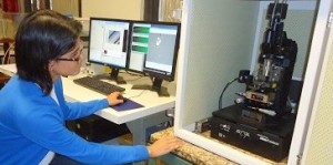
Camilla Oliveira was at the Federal University of Minas Gerais (UFMG), in Brazil, studying samples of hexagonal boron nitrite (hBN) with an atomic force microscope (AFM) within the framework of her doctoral studies in Physics, when one particular aspect of the control samples caught her attention and that of her advisor, Professor Bernardo Neves. After undergoing a heat treatment (annealing), the hBN had gained nanometric wrinkles, arranged in a geometric pattern that seemed to follow some sort of organization.
The researchers decided to study these wrinkles in more detail. They had an important question to answer: was there any relation between the arrangement of the wrinkles and the hBN crystal structure? In other words, did these wrinkles have a crystallographic orientation? Until that moment, there were no records in scientific literature of crystallographically-oriented wrinkles in two-dimensional materials, but this property could be useful.
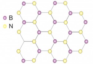
Camilla and her advisor joined other scientists from UFMG and the neighbor Federal University of Ouro Preto (UFOP) in order to carry out that research. The team produced samples composed of a few layers of hBN anchored on a silicon substrate, they heated them at 1,000 degrees Celsius and then cooled them. During this process, the silicon and the boron nitride displayed opposite strain behaviors. Due to the heating, the hBN contracts itself, while the silicon expands, shrinking the hBN. On the other hand, the cooling expands the hBN and shrinks the silicon, folding the boron nitride as origami paper.
After much experimental work using several techniques and approaches, and various simulations, the scientists were able to confirm that the wrinkles were forming in well-defined directions inside the crystal lattice. Analyzing the folding pattern in details, the scientists noticed the triangular-shaped joints by which the wrinkles (usually three of them) met.
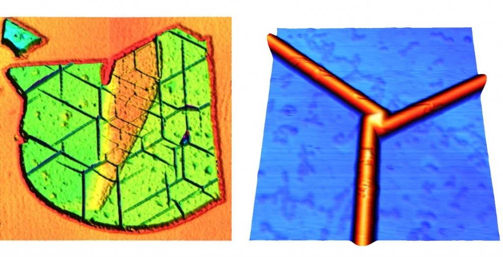
Detail: as proven by the Brazilian scientists, for the crystallographically-oriented folding patterns to be formed, the heat treatment must consist of rapid heating, followed by slow cooling (for example, citing the rates used in the research, 50 °C per minute to heat, and 8 °C per minute to cool). The wrinkles produced with faster cooling rates are arranged in a disorderly manner, with no crystallographic orientation.
The researchers have also concluded that this type of organized strain could happen, not only to hBN, but to other two-dimensional materials as well, such as graphene, and that it could lead to interesting applications in straintronics – the field of knowledge that studies and explores the capacity of some materials to have their properties deeply changed due to strain processes.
The results of the research were recently published on the scientific journal Nano Research.
“In my opinion, the main contribution of the paper is to present a property that may be shared by many two-dimensional materials: the organized strain, i.e., strain in well-defined crystallographic directions, of a material at the nanoscale”, says Professor Neves, who is the corresponding author of the paper.
The research was funded by the Brazilian agencies Capes, CNPq and Fapemig, and by INCT-Nanocarbono.