Paper: Crystal-oriented wrinkles with origami-type junctions in few-layer hexagonal boron nitride. Oliveira, Camilla K.; Gomes, Egleidson F. A.; Prado, Mariana C.; Alencar, Thonimar V.; Nascimento, Regiane; Malard, Leandro M.; Batista, Ronaldo J. C.; de Oliveira, Alan B.; Chacham, Helio; de Paula, Ana M.; Neves, Bernardo R. A. Nano Research. 2015, 8(5): 1680–1688. DOI: 10.1007/s12274-014-0665-y.

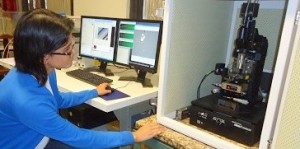
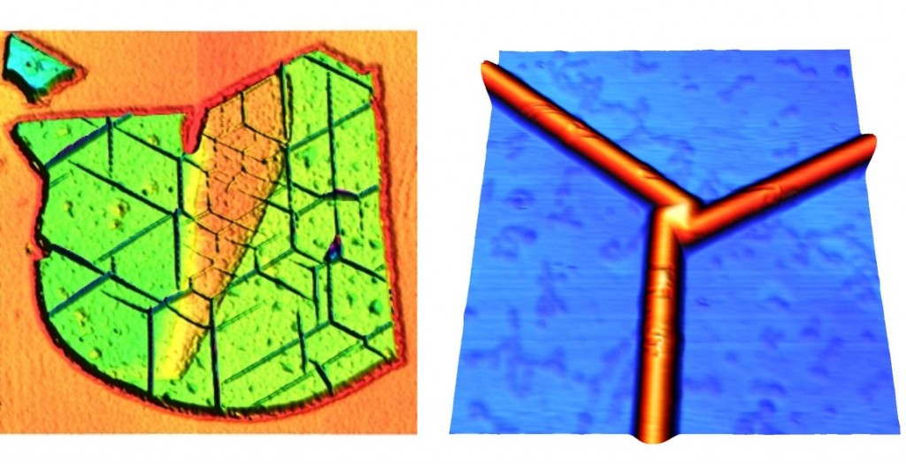
Camilla Oliveira was at the Federal University of Minas Gerais (UFMG), in Brazil, studying samples of hexagonal boron nitrite (hBN) with an atomic force microscope (AFM) within the framework of her doctoral studies in Physics, when one particular aspect of the control samples caught her attention and that of her advisor, Professor Bernardo Neves. After undergoing a heat treatment (annealing), the hBN had gained nanometric wrinkles, arranged in a geometric pattern that seemed to follow some sort of organization.
The researchers decided to study these wrinkles in more detail. They had an important question to answer: was there any relation between the arrangement of the wrinkles and the hBN crystal structure? In other words, did these wrinkles have a crystallographic orientation? Until that moment, there were no records in scientific literature of crystallographically-oriented wrinkles in two-dimensional materials, but this property could be useful.

Camilla and her advisor joined other scientists from UFMG and the neighbor Federal University of Ouro Preto (UFOP) in order to carry out that research. The team produced samples composed of a few layers of hBN anchored on a silicon substrate, they heated them at 1,000 degrees Celsius and then cooled them. During this process, the silicon and the boron nitride displayed opposite strain behaviors. Due to the heating, the hBN contracts itself, while the silicon expands, shrinking the hBN. On the other hand, the cooling expands the hBN and shrinks the silicon, folding the boron nitride as origami paper.
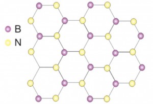
After much experimental work using several techniques and approaches, and various simulations, the scientists were able to confirm that the wrinkles were forming in well-defined directions inside the crystal lattice. Analyzing the folding pattern in details, the scientists noticed the triangular-shaped joints by which the wrinkles (usually three of them) met.

Detail: as proven by the Brazilian scientists, for the crystallographically-oriented folding patterns to be formed, the heat treatment must consist of rapid heating, followed by slow cooling (for example, citing the rates used in the research, 50 °C per minute to heat, and 8 °C per minute to cool). The wrinkles produced with faster cooling rates are arranged in a disorderly manner, with no crystallographic orientation.
The researchers have also concluded that this type of organized strain could happen, not only to hBN, but to other two-dimensional materials as well, such as graphene, and that it could lead to interesting applications in straintronics – the field of knowledge that studies and explores the capacity of some materials to have their properties deeply changed due to strain processes.
The results of the research were recently published on the scientific journal Nano Research.
“In my opinion, the main contribution of the paper is to present a property that may be shared by many two-dimensional materials: the organized strain, i.e., strain in well-defined crystallographic directions, of a material at the nanoscale”, says Professor Neves, who is the corresponding author of the paper.
The research was funded by the Brazilian agencies Capes, CNPq and Fapemig, and by INCT-Nanocarbono.
