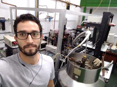
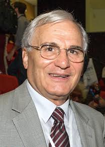
Bruno da Silva in a research laboratory in 2019, during his doctorate.
At the beginning of 2020, Bruno César da Silva was very excited. After six months of participating in an international selection process, he had obtained a position as a temporary researcher at a research institute in the city of Grenoble (France). Paid by the French government, he would commit to studying in detail the properties of semiconductor nanowires and some of their possible applications. In fact, these tiny wires may be used in future electronic and optoelectronic devices, but, for that, they need to be better understood and controlled.
In his master’s and doctorate in Physics, carried out at UNICAMP, Bruno had studied semiconductor nanowires, always under the guidance of excellent professors, and he had acquired solid knowledge in the set of techniques required by the post. “Finding someone who has a background in all the topics the job asked for is difficult, but I was lucky, was willing and had the opportunity to gain experience in all these areas,” says Bruno. In addition, Bruno is the main author of two articles published in renowned scientific journals (Nano Letters and Scientific Reports). Despite not having an expressive number of articles, Bruno’s production, generated during his doctorate, drew attention for its quality.
But Bruno’s training in scientific research started in high school, within the Junior Scientific Initiation Program of CNPq (the main federal research agency in Brazil). He then continued his undergraduate studies in Physics at the University of Lavras, where he undertook undergraduate research as a fellow of FAPEMIG (the research foundation in Minas Gerais State). While still an undergraduate student, Bruno had his first international research experience, at a Spanish university, as a fellow of the Science without Borders Program, from the Brazilian government. “My training is the result of public policies and investments,” says Bruno. In fact, at all stages, Bruno had scholarships financed with public resources. He started with less than 100 reais in high school and reached about 3,600 reais at the end of his doctorate with a scholarship from FAPESP, the São Paulo State research foundation.
Sudden change of plans
Bruno had a flight ticket and accommodations booked to begin his life in Grenoble when in mid-March the WHO declared the Covid-19 pandemic. As a result, hiring at the research institute was suspended, and Bruno started looking for other opportunities.
He searched in Brazil and abroad. He sought postdoctoral fellowships and jobs as a researcher or data scientist – a professional area linked to mathematics and computing.
Without opportunities and no income, Bruno, aged 32, returned to his parents’ home in Jacareí (SP). He requested emergency government assistance and pledged to finalize scientific articles based on the doctoral results, while taking online courses to redirect his career.
Finally, six months after the scheduled date, Bruno took on his temporary position at the French research institute. And he has been working with nanowires for over a month, very happy. “Here, we, the newly graduated doctors, are treated like professionals, and we pay taxes like any worker,” he jokes, making an implicit comparison with the situation that young PhD grant holders experience in Brazil.
After his experience in Grenoble, he plans to participate in a selection process to become a research professor at a Brazilian university. However, Bruno says that if the situation of scarce resources for science continues in Brazil, he will continue to build a career abroad. “I think it is important to return the investment in my education to the Brazilian society through teaching and conducting research that can contribute to the development of my country. We are able to do quality science in Brazil, but we need the necessary conditions,” he concludes.
[Paper: Effect of the incorporation of poly(ethylene oxide) copolymer on the stability of perovskite solar cells. Jeann Carlos da Silva, Francineide Lopes de Araújo, Rodrigo Szostak, Paulo Ernesto Marchezi, Raphael Fernando Moral, Jilian Nei de Freitas and Ana Flávia Nogueira. J. Mater. Chem. C, 2020,8, 9697-9706].
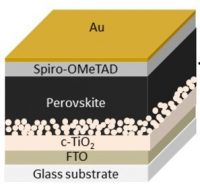
“Sandwich” of materials that form the perovskite solar cell developed by the Brazilian team.
Thanks to the contributions of research groups from different countries, perovskite-based solar cells have quickly become competitive in terms of energy conversion efficiency – the percentage of solar energy that is converted into electrical energy – reaching values above 25%. Unfortunately, the good efficiency achieved for these solar cells does not remain throughout their use, mainly because of the instability of their active layer. Composed of materials from the perovskite family, this layer of the sandwich-like solar cell is responsible for absorbing light. Due to moisture, as well as light itself, perovskite degrades and threatens the life cycle of a solar cell.
The problem has been the focus of many researchers in the area, among them, those from the Laboratory of Nanotechnology and Solar Energy (LNES) at Unicamp (Brazil), led by Professor Ana Flávia Nogueira. In recently reported research in the Journal of Materials Chemistry C (impact factor 7.059), LNES members were able to produce more stable perovskite films which allowed manufacturing solar cells with lower efficiency losses over time.
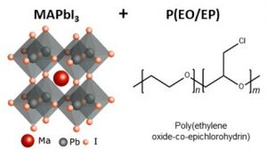
The addition of copolymer P(EO/EP) improved the stability of MAPbI3 perovskite.
The strategy adopted was to add to the perovskite a compound that gives it stability without affecting its crystalline structure, from which important properties emerge for solar cell performance. The chosen additive, a copolymer (polymer formed by two different monomers), was added in different concentrations to a solution of lead iodide and methylammonium iodide, which, when crystallized, formed a modified and more stable perovskite film.
The researchers used the spin coating technique to prepare filmes of pure perovskite and “additivated” perovskite. In a material degradation test, the authors exposed the samples to ambient light and humidity for nine days and observed their degradation, which was visible to the naked eye by the yellowing of the films, whose original color is almost black. In the samples with additive, the degradation was delayed by a few days when compared to the pure perovskite samples.
Another test carried out by the team showed the films’ ability to regenerate after an initial degradation caused by exposure to a humidifier. The samples with the additive not only degraded less, but also spontaneously regenerated, almost entirely, thirty seconds after removing the moisture source – a phenomenon known as healing – as can be seen in this video.
“This work demonstrated that incorporating a copolymer based on poly(ethylene oxide) to the perovskite layer can delay and, in some cases, even reverse the degradation process of the film with relation to moisture and lighting,” summarizes Jeann Carlos da Silva, co-author of the article.
To study in detail the structure and composition of the films, the authors used a series of characterization techniques, including an X-ray diffraction technique (in situ GWAXS), available at the Brazilian National Synchrotron Light Laboratory (LNLS), which allowed to monitor the manufacturing process of the films. Based on the set of characterization results, the authors were able to explain the mechanism that generates the protective effect in perovskite films with additives. According to them, the effect occurs mainly due to the interaction performed by the copolymer, through hydrogen bonds, with the methylammonium cation of the perovskite. In films without the additive, light and moisture cause part of the methylammonium to shift into the gas state and then leave the perovskite structure, generating the degradation, which is partially irreversible. In the films with the additive, the copolymer retains the methylammonium, which generates films that are more stable and have greater regenerative capacity.
“This study also allowed to investigate the crystallization dynamics of the perovskite containing the copolymer, as well as to understand the formation mechanisms of perovskite/copolymer in humidity and lighting conditions,” highlights Francineide Lopes de Araújo, co-author of the article. “In addition, through characterization techniques such as in situ X-ray diffraction, the study explores an important area in order to understand the material, offering an important contribution to the scientific community and opening new investigation perspectives for the application of polymers in the process of forming and manufacturing perovskite solar cells,” she adds.
Finally, the scientific team manufactured solar cells using perovskite films with and without additives as active layer, and compared their energy conversion efficiency. Initially, the presence of the copolymer decreased the efficiency of the devices, since, as it is an insulating material, it impairs the transfer of electrical charges. However, in the stability tests, when the devices were exposed to humidity and light for twenty days, the perovskite cells with additives performed better.
In numbers: while pure perovskite solar cells started at 17% efficiency and maintained 47% of that value at the end of the test, perovskite devices containing 1.5 mg mL-1% copolymer had an initial efficiency of around 15 %, but retained 68% of efficiency after the 20 days of testing.
“Unfortunately, the problem of stability of perovskite solar cells could not be definitively solved through this research, however, an important way to protect the material was explored, mainly against aggressive exposure to moisture and light, which in the future can be combined with other protection mechanisms,” summarizes Jeann Carlos da Silva. “The research also reinforces the feasibility of incorporating extrinsic compounds to perovskite as protective agents,” he adds.
This study began at LNES in 2016, in the master’s research of Jeann Carlos da Silva, shortly after the development, in that same laboratory, of the first perovskite solar cell prototype in Brazil. The research was completed with the collaboration of the postdoctoral fellow Francineide Lopes de Araújo and other members and former members of the group, always under the guidance of Professor Ana Flávia.
The study was funded by Brazilian agencies FAPESP, CNPq and CAPES, and is the subject of the project “Perovskite Solar Cells for Artificial Photosynthesis” of the Center for Innovation on New Energies (CINE) with support from Shell and Fapesp.
Authors of the paper. From the left: Jeann Carlos da Silva, Francineide Lopes de Araújo, Rodrigo Szostak, Paulo Ernesto Marchezi, Raphael Fernando Moral, Jilian Nei de Freitas and Ana Flávia Nogueira.
Professor Ana Flávia Nogueira (UNICAMP), B-MRS member, joined this year the advisory boards of two renowned journals in the field of Materials, both from the Royal Society of Chemistry (RSC). These are the Journal of Materials Chemistry A(impact factor = 11.301), where the Brazilian scientist is the only representative from Latin America, and Journal of Materials Chemistry C (impact factor = 7.059), where Professor Ana Flávia and Professor Carlos Graeff, also a B-MRS member, are the only scientists from Latin American institutions.
Bacterial biofilms are formed by communities embedded in a self-produced polymeric matrix forming a three-dimensional structure. Biofilms grow attached to the most diverse surfaces, natural or artificial, and can include a variety of bacteria and fungi. When found on our teeth, these microbial communities can cause well-known health damage, such as dental caries. Even inside the mouth, where biofilms tend to form, dental implants can also be harmed by the action of biofilms. In fact, the main cause of failure in dental implants is related to infections in the tissues surrounding the implant, due to bacterial accumulation on the titanium screws implanted by a surgeon dentist in the jaw bone or maxilla to support the dental prosthesis.
In light of this problem, a team of researchers from areas related to dentistry and materials developed a coating capable of reducing the adhesion of bacteria and fungi to the titanium surface, thus attacking the formation of biofilms in its initial stage. In the new coating, the bacterial adhesion was eight times less than in uncoated titanium. In addition, the coating changed the composition of the microbial population in the biofilms that appeared on the surface. Thus, the presence of bacteria directly responsible for generating infections around the implants was seven times less in the coating than in the uncoated titanium. “Our coating not only reduced the adhesion of microorganisms, but also modified its composition to a less aggressive host profile,” summarizes professor Valentim Adelino Ricardo Barão (UNICAMP), corresponding author of the paper related to the study, recently published in ACS Applied Materials and Interfaces. Finally, in addition to generating antibiofilm properties on titanium, the coating maintained this material’s biocompatibility, allowing the growth of human cells on its surface, and increased its resistance to corrosion.
According to the authors of the work, this new coating may be a promising strategy to control the formation of biofilms in titanium implants and thus reduce the development of microbial infections. “Countless coatings have been developed in this area,” contextualizes Professor Barão. “However, the ones available on the market aim, mainly, to improve biomechanical properties and biocompatibility, but not effective in reducing the accumulation of microorganisms.” According to the authors of the article, in order to apply coated titanium to patients and make it available on the market, it would be necessary to test its insertion as a dental implant in animal models and, finally, to conduct a controlled clinical trial that contemplates the insertion of the material in humans.
From developing the material to in vitro and in situ studies
The authors of the paper. From the left: Joao Gabriel Silva Souza, Martinna M. Bertolini, Raphael Cavalcante Costa, Jairo Matozinho Cordeiro, Bruna Egumi Nagay, Amanda B Almeida, Belén Retamal-Valdes, Francisco Nociti, Magda Feres, Elidiane Cipriano Rangel, and Valentim Adelino Ricardo Barao.
The research was carried out within the doctorate of João Gabriel Silva Souza, with guidance from Professor Barão and funding from Brazilian agencies Fapesp and Capes. The thesis was defended in 2019 in the Graduate Program on Dental Clinic of the School of Dentistry at UNICAMP Piracicaba.
The main objective of the thesis, says Souza, was to develop a coating for titanium, a widely used material in dentistry, that has the ability to reduce microbial accumulation by using low-pressure plasma technology. Bibliographic searches have shown that a superhydrophobic surface would be a promising alternative to reduce the adhesion of bacteria to titanium and its alloys. A surface is considered to be superhydrophobic (that is, very difficult to wet) when the angle formed between it and a drop of water is greater than 150º. Superhydrophobicity, in turn, is based on high surface roughness and chemical composition.
“Based on this idea and previous studies already developed by Professor Barão’s research group, we aimed to develop a superhydrophobic coating with plasma technology, changing various parameters, such as pressure, gases, etc.” says Souza.
The coating was developed and characterized at the Laboratory of Technological Plasmas – UNESP – Sorocaba, which includes the Multi-User Laboratory for Characterization of Materials, under the guidance of Professor Elidiane Rangel. “Professor Elidiane has broad experience in the area and has been contributing extensively to our research group in the development of coatings for dental applicability,” explains Professor Barão.
While the scientific literature recorded superhydrophobic coatings manufactured mainly in two stages (one to obtain roughness and the second to achieve hydrophobicity), Professor Rangel manufactured the coating in just one step, using the technique of PECVD (plasma-enhanced chemical vapor deposition). In this technique, an atmosphere of carefully selected gases is formed inside a reactor (in this case, oxygen, argon and hexamethyldisiloxane, of the formula C6H18OSi2). This atmosphere is highly energized (in a plasma state) after applying an electrical voltage, when the gases decompose and generate species (atoms, molecules, ions) with great propensity to react chemically. These species form new compounds that are deposited in a solid state on the surface of the material to be coated (in this case, titanium).
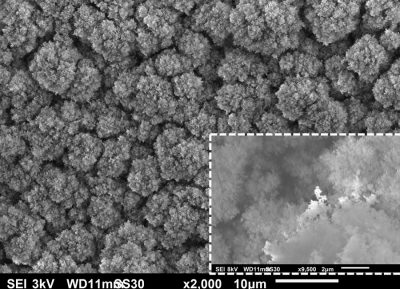
To manufacture the superhydrophobic coating using this technique, Professor Elidiane carried out a unique 60-minute process. The result was a surface based on silicon and oxygen, similar in appearance to cauliflower, with a different roughness. Making an analogy with the relief of our planet, the coating presented, on the micrometric scale, mountains of different heights and shapes, separated by valleys and canyons.
After obtaining the coating, in order to test its effectiveness as an antibiofilm, the study involved research groups from the University of Guarulhos and the University of Connecticut Health Center (USA), where the then doctoral student Souza carried out a doctoral internship.” In addition, the Brazilian National Nanotechnology Laboratory (LNNano) and the Brazilian Biosciences National Laboratory (LNBio) were used to characterize the coating and analyze the composition of adhered proteins, respectively.
The team of scientists then carried out a series of microbiological tests and analyses, both in the laboratory (in vitro) and in the mouth of volunteers (in situ), always comparing uncoated titanium and the titanium with the superhydrophobic coating. In one of the in vitro experiments, they used natural saliva as a culture medium for several microorganisms usually found in biofilms that grow on the implants. In contact with this medium, the coated titanium samples showed a very good antibiofilm performance with respect to the uncoated titanium: the adhesion of the set of microbes was eight times lower, and, in particular, the adhesion of a bacteria directly responsible for the formation of the biofilm matrix was 17 times smaller. Consequently, in a later stage of the experiment, biofilm formation in the coating was scarce and sparse.
In another interesting test, carried out in situ, four volunteers used a device on the palate during 3 days. This device was made with some untreated titanium discs and others with a superhydrophobic coating. When analyzing the composition of biofilms formed on the two surfaces, with the collaboration of professor Magda Feres of the University of Guarulhos, the researchers were once again surprised by the positive performance of the developed coating, which reduced by seven times the presence of pathogens directly associated with infections that lead to dental implant failures.
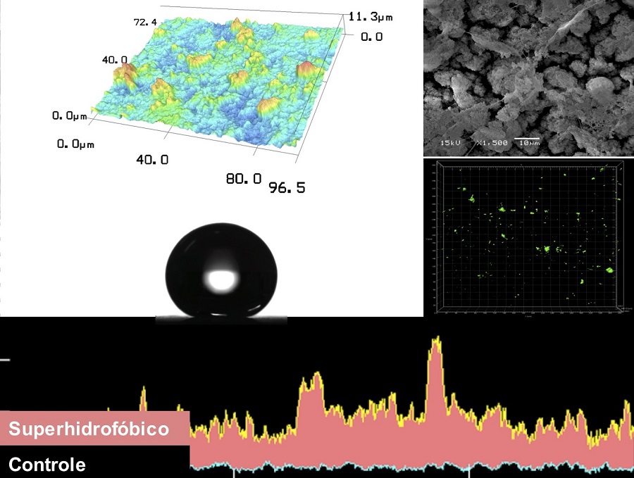
Above and to the left, 3D reconstruction based on confocal laser microscopy shows the dense formation of peaks in the new coating. High roughness with respect to uncoated titanium (control) can also be seen below. In the center, the obtained superhydrophobicity: the drop of water does not spread on the surface. On the right, images show the coating with proliferation of human cells, showing biocompatibility (above) and with reduced bacterial accumulation (green spots), below.
Cover of ACS Applied Nano Materials features the paper.
In research carried out in a number of Brazilian laboratories, a multidisciplinary scientific team developed a magnetic, luminescent nanomaterial capable of chemically binding to molecules of interest, such as drugs or proteins. This nanomaterial also showed low toxicity in tests with living organisms. With this set of characteristics, the new material can be seen as a multifunctional nanoplatform that is promising for the development of various applications, especially in the areas of biotechnology, health and environment. The study was reported in an article published in ACS Applied Nano Materials (American Chemical Society journal released in 2018), and featured on the cover of the June issue of the journal.
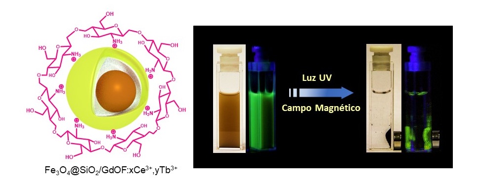
The properties of this nanoplatform derive from the presence of several compounds and elements with distinct properties: iron oxide (Fe3O4, known as magnetite) nanoparticles responsible for magnetism; lanthanide element ions (Gd3 +, Ce3 + and Tb3 +, known as rare earths) responsible for luminescence or light emission, and chitosan (biopolymer obtained from the crustacean exoskeleton), essential for providing chemical bonds of the nanoplatform surface to the external molecules of interest.
The nanoplatform was developed at the Brazilian National Nanotechnology Laboratory of the National Center for Energy and Materials Research (LNNano – CNPEM). The process used for its synthesis comprises a series of steps. Initially, the iron oxide nanoparticles that form the core of the nanoplatforms are synthesized and coated with silicon dioxide (SiO2). Then the luminescent elements and chitosan are incorporated into the nanoparticles forming an outer layer. The result is nanoplatforms of approximately 170 nm in diameter (on average), called Fe3O4@SiO2/GdOF:xCe3+,yTb3+.
On the left, a schematic illustration of one of the nanoplatforms, showing its core. On the right, a solution with nanoplatforms under the effect of a magnetic field (concentrated near the magnets) and irradiated with UV light (generating the emission of green light).
To study the magnetic and luminescent properties of the nanoplatform and to characterize its structure and morphology, research groups from the State University of Campinas (Unicamp) and the University of São Paulo (USP) participated in the study.
In addition, the main authors of the paper decided to evaluate the toxicity of nanoplatforms with relation to living organisms – a key step when thinking about health or environmental applications, and they decided to conduct a well-established in vivo test, in which zebrafish embryos (scientific name Danio rerio) are exposed to the material whose toxicity is to be evaluated. These freshwater fish, in fact, has a high genetic similarity to humans (about 70%) and at the same time is cheaper and easier to study than mice or rats, among other advantages.
In the toxicity test, a few dozen freshly fertilized zebrafish eggs were placed in aqueous medium containing the nanoplatforms at various concentrations. The embryos were examined at different development stages using an optical microscope to check for mortality, malformation, edema or changes in size. Tests included embryos with and without chorion (membrane that protects the embryo in the early stages of development). The test results carried out at LNNano showed that nanoplatforms, even at high concentrations (100 mg/L), have low toxicity for all embryo groups.
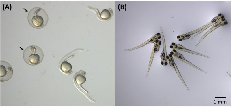
Zebrafish embryos used in nanotoxicity tests. (A) 24-hour embryos in the presence and absence of the chorion, where arrows indicate the chorion (membrane that protects embryos in the early stages of development). (B) Embryos after 96 hours of development.
“This work brings an unprecedented contribution that involves evaluating the toxicity of hybrid nanomaterials using the zebrafish model, a promising alternative method in nanotoxicology, and the influence of the chorion,” says Diego Stéfani Teodoro Martinez, CNPEM researcher at LNNano and one of the corresponding authors of the article.
The embryos were also analyzed at the Brazilian National Synchrotron Light Laboratory (LNLS – CNPEM) to verify the distribution and concentration of nanoplatforms in the organism of the embryos. To do this, the scientists used the synchrotron light X-ray fluorescence microscopy (SXRF) technique, which can accurately map certain chemical elements in biological systems. This technique is available at one of the LNLS experimental stations, coordinated by the researcher Carlos Alberto Pérez, who is one of the corresponding authors of the article.
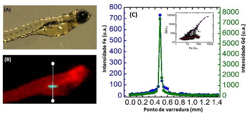
X-ray fluorescence microscopy analysis with synchrotron light (SXRF) of two zebrafish embryos after exposure to the nanoplatform for 72 hours. (A) Optical microscopy image of the embryos; (B) SXRF image of embryos demonstrating nanoplatform accumulation in the intestinal tract; and (C) X-ray fluorescence intensity along the white line indicated in (B), demonstrating the spatial co-location of Fe and Gd elements in the intestinal tract of zebrafish embryos.
SXRF analysis showed that nanoplatforms had accumulated in the embryos as a function of exposure time, with higher concentrations in the gastrointestinal tract in the case of already developed mouth embryos – a result that may be significant, for example in the context of healthcare applications involving oral nanoplatform ingestion.
The study was carried out in the context of a postdoctoral project by fellow Latif Ullah Khan, also corresponding author of the article. The completion of the project, says Martinez, was made possible by the availability of skills and facilities at CNPEM’s multi-user laboratories. However, partnerships with other laboratories were also crucial, adds the CNPEM researcher. Professor Marcelo Knobel’s group performed the magnetometry studies at Unicamp. The groups of professors Hermi Felinto Brito and Magnus Gidlund carried out the luminescence and functionalization studies at USP. Finally, Professor Diego Muraca (Unicamp) and researcher Jefferson Bettini (CNPEM) contributed to the structural and morphological characterization using transmission electron microscopy techniques.
“This article was the result of integrating the experience of different Brazilian groups; an interdisciplinary study on the frontier of knowledge in nanobiotechnology and nanotoxicology,” says Martinez, adding that one of the main challenges of the work was integrating knowledge and techniques from different areas, such as Materials, Biology and Toxicology, a task that was coordinated by Martinez and Pérez.
The main authors of the paper. From the left: Latif Khan, Carlos Pérez and Diego Stéfani Martinez.
The study received financial support from Brazilian agencies CAPES (including through the CAPES-CNPEM agreement), FAPESP and CNPq (including through INCT-Inomat); from the Brazilian Ministry of Science, Technology, Innovations and Communications (MCTIC) through SisNANO, and The World Academy of Sciences for advancement of science in developing countries (TWAS). The study also received financial support from the Brazil-China Nanotechnology Research and Innovation Center (CBC-Nano).
Applications: biotechnology, health and the environment
According to Martínez, the nanoplatform developed opens perspectives for applications in biotechnology, health and the environment, such as biological tissue and cell imaging systems, medical diagnostic kits, and environmental systems for pollutant detection and remediation
The applications would take advantage of the interesting set of nanoplatform properties. Because they are magnetic, using an external magnet, nanoplatforms could be directed and retained in a particular biological tissue or isolated from, for example, contaminated blood or water. In addition, the luminescence of the nanomaterial would allow visualizing the nanoplatforms within the biological tissues and cells of interest. Finally, the presence of chitosan would enable the chemical binding of drugs and other molecules that would serve for the diagnosis and/or treatment of diseases. “However, much study is still needed for real applications and commercialization of this nanoplatform, as it is a new material and needs to be tested on different models in the future,” says Martinez Martinez.
[Paper: Fe3O4@SiO2 Nanoparticles Concurrently Coated with Chitosan and GdOF:Ce3+,Tb3+ Luminophore for Bioimaging: Toxicity Evaluation in the Zebrafish Model. Latif U. Khan, Gabriela H. da Silva, Aline M. Z. de Medeiros, Zahid U. Khan, Magnus Gidlund, Hermi F. Brito, Oscar Moscoso-Londoño, Diego Muraca, Marcelo Knobel, Carlos A. Pérez, Diego Stéfani T. Martinez. ACS Appl. Nano Mater. 2019, 2,6, 3414-3425. https://doi.org/10.1021/acsanm.9b00339.]
Professor Oswaldo Luiz Alves (IQ – UNICAMP), a member of B-MRS, was awarded the title of Professor Honoris Causa of the Federal University of Ceará (UFC). The title was granted by the University Council of the institution on December 17, 2018. In addition to being a full professor of UNICAMP, Alves has been a collaborating professor of the Graduate Program in Physics of UFC for more than 30 years.
In October 2018, Professor Alves received another important distinction, the admission to the Brazilian National Order of Scientific Merit in the Grand Cross class.
[Paper: Evidence of Band-Edge Hole Levels Inversion in Spherical CuInS2 Quantum Dots. Gabriel Nagamine, Henrique B. Nunciaroni, Hunter McDaniel, Alexander L. Efros, Carlos H. de Brito Cruz, and Lazaro A. Padilha. Nano Lett., 2018, 18 (10), pp 6353–6359. DOI: 10.1021/acs.nanolett.8b02707]
Quantum dots with unique rules
A paper led by Brazilian researchers has revealed surprising news about the rules that determine the energy levels of electrons in quantum dots of copper and indium disulphide (CuInS2,) which stand out in the family of quantum dots for being non-toxic. The work was recently reported in Nano Letters (impact factor of 12.08).
The results of the study, confirmed by experimental and theoretical methods, showed a situation in the structure of energy bands that had never before been observed in other materials.
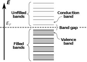
Simple diagram of semiconductor band structure. Credits
The band structure is a well-established scientific model that shows which energy states or levels the electrons can occupy in a given material. These states of energy are represented as allowed bands (those that the electrons can reach) and forbidden bands (those in which the electrons cannot be found).
In semiconductors, the energy bands that are allowed for an electron and that determine the properties of a material are the valence band and the conduction band. Both are separated by a band gap. For electrons to “jump” from the valence band to the conduction band, transposing the forbidden band in a process called transition, it is necessary they receive extra energy, which can occur when the material absorbs photons. When they lose energy, these electrons can once again occupy their places in the conduction band, and surplus energy can be emitted as photons (light). This light emission from the absorption of photons is known as photoluminescence.
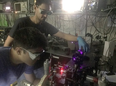
Photo of the students Gabriel Nagamine (front) and Henrique Nunciaroni, the first authors of the paper, working in the laboratory.
Researchers at the Gleb Wataghin Institute of Physics at UNICAMP (Campinas, SP, Brazil) discovered that the quantum dots they were studying did not follow the same transition rules as other semiconductor materials and nanomaterials. “Generally, in semiconductors, bulk or nanostructured, the states that form the top of the valence band and the bottom of the conduction band are such that a transition between these states by absorption of a photon is allowed,” contextualizes Lázaro Aurélio Padilha Junior, professor at UNICAMP and corresponding author of the article. “What we showed was that in the studied material (CuInS2 quantum dots), this transition is forbidden by absorbing one photon. The interaction with two photons is required for this transition to occur. As far as we know, this is the first semiconductor system that presents this inversion of states,” says Padilha.
The discovery, besides showing that the norms that govern the electron states in semiconductors are not valid for all the materials, can influence the applications of the quantum dots studied. According to Padilha, the conditions discovered favor the simultaneous emission of two photons in the material when the electrons return to the conduction band. “This could be attractive to lasers systems that emit light in two distinct colors at the same time, and with color adjustment over a wide spectral range,” says the professor. In addition, adds Gabriel Nagamine, the first author of the article, understanding the structure of material bands can improve the performance of existing applications such as luminescent solar concentrators – a technology that can be used both to generate electricity from sunlight and to increase the production of food in greenhouses. “All these applications come from the unique characteristics of the electronic bands of these materials,” says Nagamine.
History of a theoretically announced experimental result
The history of this discovery goes back to 2015, when Professor Padilha, who has worked with quantum dots since 2010, his master’s student Gabriel Nagamine and other members of the research group decided to devote their efforts in studying the quantum dots of CuInS2. “This material caught our attention because it did not have heavy metals in its composition, which made it interesting for applications in biology and medicine, such as fluorescent biological markers,” says Padilha. In fact, quantum dots, which were discovered in the 1980s and are now present in products such as TV screens, present very interesting properties to be used in the detection of diseases and other applications in the health area, but almost all of them are toxic due to their chemical composition.
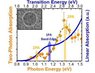
Two-photon (yellow dots) and one-photon (blue line) absortion spectra in spherical CuInS2 quantum dots. Arrows: absortion peaks of two photons (yellow) and one photon (blue). In the upper left corner, TEM image showing one of the quantum dots.
The UNICAMP team then collaborated with the company UbiQD, located in Los Álamos (USA) and specialized in the production of quantum dots, and which provided samples of spherical and pyramidal quantum dots. The characterization of the samples was performed partly in the company and also in the National Nanotechnology Laboratory (LNNano) of CNPEM, in the city of Campinas (SP, Brazil).
Initially, Padilha and his team set out to investigate how strong the absorption of two photons was in the chosen material, since this optical process allows to make three-dimensional images of the material, which can be very useful in its characterization and also in its application in several areas. To do this, in early 2016, the team performed the main experiments of the work at UNICAMP using a spectroscopy technique that allows detecting light emission from the absorption of two photons. “The first measurements revealed an absorption peak of two photons at smaller energies than those of linear absorption – a fact never previously observed experimentally,” Padilha says. “We believed it was a problem in our laser source and we repeated the experiment, achieving the same results,” he adds. These results, which are shown in the figure to the side, have arisen from the experiments performed with spherical quantum dots. In the pyramid-shaped quantum dot samples, the predominance of of two-photon absorption was not observed.
In May of the same year Padilha met with Dr. Alexander Efros (Naval Research Laboratory, USA) at a conference in South Korea. “He, who is one of the most respected theorists working on the electronic structure of semiconductor quantum dots, mentioned that he had made calculations that predicted a reversal in parity of states in these nanomaterials. We immediately noticed that I had proven his theory, “says Prof. Padilha. After that, they began working together and trying to understand other aspects of the problem, until they submitted the article to Nano Letters. The paper was accepted in less than two months.
The research that originated the paper is part of Gabriel Nagamine’s master’s thesis, defended in 2017 at UNICAMP, and received financial support from Brazilian research agencies (FAPESP and federal CNPq), the student support service (SAE) of UNICAMP and the Office of Naval Research (USA).
Fernando Galembeck’s interest in research began in adolescence, when he realized the economic value of scientific knowledge while working in his father’s company in the pharmaceutical segment. Today, at age 75, Fernando Galembeck can look back at his own scientific trajectory and tell many stories about the generation and application of knowledge.
A founding member of B-MRS, Galembeck was chosen this year to deliver the Memorial Lecture “Joaquim da Costa Ribeiro” – a distinction awarded annually by B-MRS to the trajectory of a distinguished researcher in the Materials area. The honor is also a tribute to Joaquim da Costa Ribeiro, pioneer of experimental research in Materials in Brazil. The lecture, titled “Materials for a better future,” will take place at the opening of the XVII B-MRS Meeting on September 16 of this year, and will address issues such as needs, shortages and promises in the Materials area.
Galembeck graduated in Chemistry in 1964 from the University of São Paulo (USP). After getting his degree, he remained at USP working as an instructor (1965-1980) while doing his Ph.D. in Chemistry (1965-1970), in which he developed research on dissociation of a metal-metal bond. After his Ph.D., he completed post-doctoral internships in the United States, at the universities of Colorado, in the city of Denver (1972-1973) and California, in the city of Davis (1974), working in the field of Physical-Chemistry of biological systems. In 1976, back at USP, he had the opportunity to create a laboratory of colloids and surfaces at the Institute of Chemistry, in an agreement that involved the Institute, Unilever, the Brazilian Academy of Sciences and the Royal Society. From that moment on, Galembeck became more and more involved with the development of new materials, especially polymeric materials, and their manufacturing processes.
In 1980, he joined the State University of Campinas (Unicamp), after which he became a full professor in 1988, where he remained until his retirement in 2011. Since then, he has been a contributing professor at the institution. At Unicamp, he held management positions, notably vice-rector of the university, as well as director of the Institute of Chemistry and coordinator of its post-graduate program. In July 2011, he took over the newly created Brazilian National Nanotechnology Laboratory (LNNano), at the National Center for Energy and Materials Research (CNPEM), remaining in this post until 2015.
Throughout his career, he has held direction or coordination positions at the Brazilian Academy of Sciences (ABC), the Ministry of Science, Technology and Innovation (MCT), the National Council for Scientific and Technological Development (CNPq), Sao Paulo Research Foundation (FAPESP), Brazilian Chemical Society, (SBQ), Brazilian Society for the Advancement of Science (SBPC) and the Brazilian Society of Microscopy and Microanalysis (SBMM), among other entities.
Prof. Galembeck is the author of roughly 279 scientific papers published in peer-reviewed journals, with over 3,700 citations, 35 patents and more than 20 books and book chapters. He has supervised nearly 80 master’s and doctoral degrees.
Fernando Galembeck received numerous awards and distinctions, among them the Anísio Teixeira Award, from CAPES, in 2011; the Telesio-Galilei Gold Metal 2011, from the Telesio-Galilei Academy of Science (TGAS), the Almirante Álvaro Alberto Award for Science and Technology 2006, from CNPq and the Conrado Wessel Foundation; the José Pelúcio Ferreira Trophy, from Finep, in 2006; the Grand Cross of the National Order of Scientific Merit, in 2000, and the National Commendation of Scientific Merit, in 1995, both from the Presidency of the Republic of Brazil. He also received a series of acknowledgments from companies and associations, such as CPFL, Petrobrás, Union Carbide do Brasil, the Brazilian Association of Paint Manufacturers, the Brazilian Chemical Industry Association, the Union of Chemical Industry for Industrial Purposes of the State of Rio de Janeiro, Brazilian Polymer Association, Brazilian Chemical Society (which created the Fernando Galembeck Technological Innovation Award), the Union of Engineers in the State of São Paulo and the Electrostatic Society of America.
This scientist has been a fellow of TWAS (The World Academy of Sciences) since 2010 and from the Royal Society of Chemistry since 2014.
In this interview, you will be able to know a little more about this Brazilian researcher and his work.
SBPMat Newsletter: – Tell us what led you to become a scientist and work on issues in the field of Materials.
Fernando Galembeck: – My interest in research work started during my adolescence, when I comprehended the importance of new knowledge, of discovery. I found this when I was working, after school, at my father’s pharmaceutical laboratory, as I could see how the newest, latest products, were important. I also saw how costly it was, for the lab, to depend on imported raw materials, which were not produced in Brazil, and that in the country there was no competence to manufacture them. Then I realized the value of new knowledge, as well as the importance and the economic and strategic significance of such breakthroughs.
This feeling was increased when I took my major in Chemistry. I enrolled into the Chemistry course because one of my school teachers had suggested that I should seek a career related to research. He must have seen some inclination, some tendency of mine. So I attended the Chemistry course provided by the Philosophy School, in an environment where the research activity was very vivid. Because of that, I decided to conduct my Doctoral studies at USP. At that time, there were no regular graduate studies in Brazil yet. The advisor with whom I defended my dissertation, Professor Pawel Krumholz, was a great researcher, who also had built a very important career working on a company. He was the industrial director of Orquima, a major company by that time. That boosted my interest in research.
I worked with Chemistry for some years and my interest in materials came from a curious occurring. I was almost graduating, in my last vacations during the undergraduate studies. I was at an apartment, resting after lunch. I remember looking at the walls of this apartment and noticing that, with all I had learned in the Chemistry course, I did not have much to say about the things I could see: the paint, the coverings etc. That was Chemistry, but also Materials, and there was not much interest in Materials in the Chemistry course. Actually, Materials became very important in Chemistry mainly because of plastic and rubber, which, at the time, did not have the importance they have today. I’m talking about 1964, when petrochemicals were practically non-existent, in Brazil.
Well, then I started to work with Physical Chemistry, to later work a little in a field that is more oriented to Biochemistry, that is Biological Physical Chemistry and, in 1976, I received a task from the USP Department, which was to build a colloids and surfaces laboratory. One of our first projects was to modify plastic surfaces, in that case, Teflon. Then I realized that a major part of the colloids and surfaces Chemistry existed due to Materials, because the subject lends itself to create and develop new materials. From that moment on, I was getting increasingly involved with Materials, mainly polymers, a little less with ceramics, and even less with metals.
SBPMat Newsletter: – What are, in your own opinion, your main contributions to the field of Materials? Consider, in your answer, all aspects of your professional activity, including cases of knowledge transfer to the industry.
Fernando Galembeck: – I will tell the story in order, more or less. I think that the first important result in the field of Materials was exactly a technique intended to modify the surface of Teflon, that material in which it is very difficult to stick something. There is even that expression, “Teflon politicians”, the ones for which does not matter what you throw at them, they do not stick to anything. But, in certain situations, we want the Teflon to have adhesion. So, by a somewhat complicated path, I managed to see that I already knew how to modify Teflon, but I had never realized that is was important. I knew the phenomenon; I had observed it during my PhD defense. I knew that there was a change happening in Teflon. But it was during a visit to a Unilever laboratory in 1976, when I was talking to a researcher, that I saw that there were people striving to modify the surface of Teflon and achieve adhesion. Then, bringing the problem and the solution together, as soon as I returned to Brazil, I tried to see if I what I had previously observed was really useful, and it worked. That led to the first paper I wrote by myself and my first patent application, at a time when almost nobody talked about patents in Brazil, especially in the university environment. I was very enthusiastic about this: I was approached by companies that were interested in applying what I had done; one the modification in Teflon itself, the other in a different polymer. So I felt great, because I had made a discovery, I had a patent, and there were companies which, at least, would like to know what it was to see if there was a way to use it. One more thing: soon after the paper I wrote was published, I was invited to attend a conference in the United States, which addressed exactly the issue of modifying surfaces. Polymers, plastic and rubber surfaces, a subject with which I was involved for pretty much the rest of my life, up until now.
I will mention a second fact that did not have the same effects, so far. I discovered a method that enables the characterization and separation of very small particles. That was a very interesting paper. It was released, also produced a patent, but had no practical consequences. Recently, there have been some issues related to nanoparticles, which is a very important subject in Materials now, offering a chance to apply what I did over 30 years ago. The name of the technique is osmosedimentation.
Next there was some work that I did by collaborating in projects with Pirelli Cabos. With all this story of surfaces and polymers, I think I had become more or less known and was approached by Pirelli, which contracted me as a consultant and commissioned projects I had at Unicamp. An outcome of these projects, that I think is the most important, was the development of an insulator for very high voltages. This work was not only mine, but rather of a very large team, in which I took part. There were several people from Pirelli, and several from Unicamp. The result of this project was that the Brazilian Pirelli managed to be hired to provide high voltage cables for the Eurotunnel, back in the ‘80s. I think this was a very important case, as it led to a product and brought substantial economic results. I would like to stress that this was done in Brazil, by a Brazilian team. They were not a Brazilian company, but the team was based here.
Then I worked on several studies with nanoparticles, at a time when we did not even call them nanoparticles; we called them fine particles or simply small colloidal particles. The first work I published on nanoparticles was in 1978. There were other things I did next, which ultimately turned into a work on aluminum phosphate, which gave rise to several theses carried out in the laboratory and publications, and was also licensed by a company of the Bunge group, which basically exploits phosphates. The subject started in my laboratory, stayed in the laboratory for several years, then a company from the Bunge group here in Brazil became interested, started to participate, we collaborated. This became a rather large development project. Bunge later found the project unfeasible in Brazil and today it is the United States. I think it’s a pity that it is there, but there were other issues involved, including disagreements with Unicamp, which owns the patents. Recently, the company of the group that worked with these phosphates was Amorphic Solutions, which offered the product on the Internet, for various applications. From what I understand, they are currently emphasizing its use as an anticorrosive material for steel protection. I have recent information that Bunge has negotiated the rights to these products with a large chemical company, but I do not know the details.
About the same time, in another project on nanoparticles, clay/natural rubber nanocomposites were developed. This was licensed by a Brazilian company called Orbys, which released a product called Imbrik, that showed to be good for rubber rolls for paper manufacturing.
Another case with a product. I had done a project with Oxiteno, which manufactures raw materials for latex, the surfactants. They wanted to get an ideia of how much you can change the latex changing the surfactant. I conducted a project with them that I consider one of the most interesting among those in which I have been involved. In the end, we realized that, by changing the surfactant a bit, we changed the latex a lot. These are used in paints, adhesives, resins. So we realized we had a great versatility. This work was published and promoted. It did not result in a patent because it was a comprehension project. So, another company, Indústrias Químicas Taubaté (IQT) approached me to produce cationic latex, but using a new path. Cationic latex in general is made of quaternary ammonium salts, which have some environmental restrictions. The company wanted an alternative that did not have those restrictions. By the end of the project, we produced cationic latex without environmental restrictions, and the IQT put the product on the market.
My participation in a Navy project of developing carbon fibers was a great challenge that gave me big satisfaction. My group participated by synthesizing copolymers of acrylonitrile, up to the scale of ten liters. The results were transferred to a company that produced pilot scale production at the old Rhodia-Ster and Radicci plant in São José dos Campos. The selected copolymer was spun and then pyrolyzed, at the Technological Center of Marinha, in São Paulo. It resulted in a high performance carbon fiber, which was used in the manufacture of a centrifuge, used in Aramar. The challenge was to find the copolymer that showed good performance in the later stages of fiber production, which was achieved.
There was another case that was also very interesting, even though it was canceled. Here in Brazil, there was a large manufacturer of polyethylene terephthalate, PET, which is used for many things, including bottles. They knew about the work I had done with nanocomposites, the one with Orbys I mentioned before, so they approached me wanting to produce PET nanocomposites. We had to find out how to escape from what was already patented abroad and discovered a whole new path. The company was called Rhodia-Ster, and today it is part of another Italian company, called Mossi e Ghisolfi. The company was enthusiastic and ended up patenting it in Brazil, and then later abroad. At a certain point, they decided that they would conduct the work internally, and so they did for some years. One day, my contact within the company called me to tell this: “look, we were working with two technologies; the one held by Unicamp and another one, in another country. Both are working, but the company has reached a point where it has chosen to complete the development of only one”. When coming to the final stage in developing materials, the projects costs are too high. One have to use large amounts of materials, run many tests with customers. So, the company decided to take one project further, and, unfortunately, it was not the one in which I had worked. At the end, it was a little frustrating, but I think that it was interesting, because, during this whole time, the company invested a lot in the path we had started here. Not only that, each project brings resources for the laboratory, jobs at the university and the company etc. So, these projects result in many benefits, even when they are not concluded.
Now, fast forwarding, I will arrive at a more recent result of my work at CNPEM, where I was until 2015. A goal of CNPEM is the use of renewable source materials to make advanced materials. It has a whole philosophy behind it, related to the depletion of natural resources, to sustainability… The goal was to do new things with materials derived from biomass, and the main interest is in cellulose. It is the most abundant polymer in the world, but it is a very difficult polymer to work with. You cannot process pulp as you process polyethylene, for example. One of the goals is to plasticize cellulose; that is, to work the cellulose as closely as possible to the one we use to work with synthetic polymers. An initial result within this idea was the creation of cellulose adhesives in which the only polymer is cellulose itself. Then, by then no longer at CNPEM, we obtained graphite exfoliation, which generated a family of paints, pastes and conductive adhesives, which are the object of a PIPE project recently approved by Fapesp.
This is the latest case. In the middle of the way, many other projects were conducted with companies, for issues of their interest. Coating something, gluing another, modifying a polymer to achieve a certain result. But these were answers to demands from companies, instead of researches started at the laboratory.
SBPMat Newsletter: – Leave a message for our readers who are starting their careers as scientists.
Fernando Galembeck: – First of all, in any chosen career, there must be a dose of passion. It does not matter if you are going to work in the Stock Market, Healthcare or whatever you may do; above all, your taste must decide. If a person chooses a career because it will give them money or status… I think it is a bad choice. If you do things with pleasure, with interest, the money, prestige and status will come from other paths. The goal is to do what makes you happy, what makes you feel good when you do it, what makes you feel accomplished. It is true not only for the scientific career, but also to any other career. In science, it is crucial.
Another point is that you must be prepared to work hard. There is no easy way. I know some young people who are constantly seeking the great idea that will bring them success with relatively little work. Well, I’d better not count on it. It may even happen, but waiting for it is almost the same as wait to win the Lottery and get rich.
I’m over 75, therefore I have met many people and seen many things happen. Something that strikes me is how young people who seemed very promising end up not working very well. Frankly, I think it is bad for youngsters to achieve success too early, because I have the impression they get used to this idea that things will always work out fine. And the problem is that there isn’t anything, anyone, any company that will always work. There will always be the moment of failure, the moment of frustration. If the person is prepared for that, when the times come, he or she will overcome it, while others are crushed – they cannot move one. That is why we must be careful not to be deceived by our success and think that, because it worked once, it will always work. You must be prepared to fight.
When I was in college, thinking about doing research seemed a very strange thing to do, crazy talk. People did not know very well what it was, or why would someone choose to do it. Some people said that research was something like priesthood. I have always worked with research, associated with teaching, consulting and, without having ever sought to become rich, I managed to have an economic status that I deem very comfortable. But I insist, my goal was to enable the development, to produce material, not the money I would receive. Money came, as it does. So, I suggest you to focus on your work, on the results and the contribution that said work may give to other people, to the environment, to the community, to the country, to knowledge. The rest comes as a bonus.
In short, my message is: work seriously, earnestly and passionately.
Finally, I would like to point out that I think the research work, the development work, really helps you to grow as a person. It will depart you from ideas that are not very fruitful and guide you towards attitudes that are really important and helpful. A student asked Galileo once: “Master, what is the method?”, and Galileo’s answer was: “The method is the doubt”. I think it is very important in the research activity, which, for Materials in particular, is especially interesting because the final product is something you can hold in your hands. In the research activity you have to always wonder, “I’m thinking like this, but is this right?”, or “This guy wrote this, but what are his bases to write it?”. This attitude is very different from the dogmatic one, which is common in the realms of politics and religion, and very different from the attitude of someone who has to deceive, as the lawyer who works for a corrupt or drug dealer. The researchers have to commit themselves to the truth. Of course there are also people who call themselves researchers and spread disinformation. Some years ago, people were talking about something called “Bush science”, an expression referring to President Bush. This Bush science was the arguments fabricated by people who gained money as scientists, but who produced arguments to sustain Bush’s policies. In other words, the problem exists in science as well, but then we get back to what I said earlier. You cannot become a scientist because of money, or to achieve prestige, or to be invited to have dinner with the president; you must enter this field because of your interest in the subject itself.
[Exploring Au Droplet Motion in Nanowire Growth: A Simple Route toward Asymmetric GaP Morphologies. Bruno C. da Silva*, Douglas S. Oliveira, Fernando Iikawa, Odilon D. D. Couto Jr., Jefferson Bettini, Luiz F. Zagonel, and Mônica A. Cotta*. Nano Lett., 2017, 17 (12), pp 7274–7282. DOI: 10.1021/acs.nanolett.7b02770]
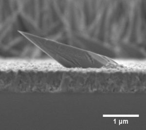
Moving nanoparticles for asymmetric nanowires.
Scanning electron microscopy image of asymmetric gallium phosphide (GaP) nanowires.
A team of scientists presented a route to grow semiconductor nanowires having an asymmetric morphology, different from the traditional cylindrical one. The possibility of producing, in a controlled manner, nanowires with particular formats and without defects, can be exploited in several applications, including the production of more efficient solar cells.
The research was led by scientists from the Brazilian university UNICAMP and the Brazilian Nanotechnology National Laboratory (LNNANO), who reported their findings in a paper in NanoLetters.
The researchers discovered the process while studying the production of nanowires of gallium phosphide (GaP) for optoelectronic applications. The team chose to produce the nanowires by chemical beam epitaxy (CBE), preceded by a thermal treatment (annealing). In this technique, a substrate of a suitable material – in this case gallium arsenide (GaAs) – is placed inside a chamber. Then, chemical compounds in the form of vapor are introduced into the chamber. Some elements of the vapored material deposit over the substrate, layer upon layer, generating films. To promote the growth of nanowires instead of films, metallic nanoparticles (in this case, gold nanoparticles) are placed on the substrate before being exposed to vapor. During exposure, these catalytic nanoparticles cause the material to deposit preferentially underneath them, causing wire-like structures to grow.
While the researchers were analyzing the nanowires they had obtained in the first few months of the work, they found a significant amount of asymmetric nanostructures. “Besides having a particular morphology, we saw that these nanowires had an hexagonal crystal structure (wurtzite) and a very low density of crystallographic defects, which motivated us to study in detail the causes for the formation of this unusual structure,” says Bruno da Silva, PhD student at UNICAMP and corresponding author of the paper.
Da Silva and his supervisor Prof. Mônica Cotta then began to raise and test hypotheses for the cause behind the formation of the peculiar structures. After several experiments and analyses, they focused on a phenomenon that caught their attention: in the early stages of the process, the gold nanoparticles spontaneously moved over the substrate. Hence, the duo undertook a systematic work on heating substrates with nanoparticle catalysts, growing nanowires under various conditions, and analyzing the resulting samples through scanning and transmission electron microscopes and atomic force microscopy.
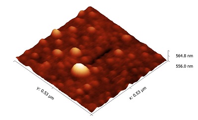
Atomic force microscopy image of a gold nanoparticle on GaAs substrate showing the trail left by its movement.
Da Silva, Prof. Cotta and their collaborators from UNICAMP and LNNano were able to find out why the growth process they used resulted in asymmetric nanowires. The main reason was the movement of the gold nanoparticles, which was thermally activated with the initial annealing. Based on that discovery, the team established a recipe for producing asymmetric semiconductor nanowires in a controlled manner. “Our work was the first to show that the mechanical instability of the nanoparticle catalyst can be used to modify the growth of semiconductor nanowires, in our case, particularly affecting their morphology,” says Bruno da Silva.
The mechanism of the asymmetric nanowires growth presented in the NanoLetters paper can be described as follow. When heated together with the substrate, the nanoparticles begin to crawl and advance through the substrate while consuming the oxide layer that naturally covers the gallium arsenide. Thus, the nanoparticles form asymmetric grooves a few nanometers deep and a few hundred nanometers long. These trails become fertile ground for the growth of the nanowires, since the deposition rate of the vapored material is greater there than in the rest of the substrate, which is covered by the oxide. A pedestal then forms along the grooves and the nanowire grows on top of the pedestal with an asymmetrical format. “We showed that the movement of the particle generates a zone of preferential deposition, and that the combination of this phenomenon with the axial growth “vapor – liquid – solid” leads to the asymmetry in the nanowire,” summarizes da Silva.
Besides describing the formation mechanism of asymmetric nanowires, the work of the Brazilian team generated detailed knowledge about the movement of heated metallic nanoparticles. “We have shown that in addition to temperature, vacuum conditions and surface quality of the substrate are crucial for nanoparticle stability, and that the motion direction is related to the asymmetry of gold dissolution on semiconductor surfaces III-V,” details the doctorate student.
Concerning possible applications, the asymmetry of these nanowires can be explored, for example, in the construction of antireflective layers that reduce the amount of light lost by reflection in solar cells. Another possibility would be to exploit the green emission of these wurtzite gallium phosphide nanowire in lighting devices. Or, why not, to develop an alternative process to electronic litography taking advantage of the gold nanoparticles movement and the trails it forms on the substrate.
The work was funded by Unicamp, the Brazilian federal agencies CNPq and CAPES and the São Paulo Research Foundation (FAPESP).

 To study in detail the structure and composition of the films, the authors used a series of characterization techniques, including an X-ray diffraction technique (in situ GWAXS), available at the Brazilian National Synchrotron Light Laboratory (LNLS), which allowed to monitor the manufacturing process of the films. Based on the set of characterization results, the authors were able to explain the mechanism that generates the protective effect in perovskite films with additives. According to them, the effect occurs mainly due to the interaction performed by the copolymer, through hydrogen bonds, with the methylammonium cation of the perovskite. In films without the additive, light and moisture cause part of the methylammonium to shift into the gas state and then leave the perovskite structure, generating the degradation, which is partially irreversible. In the films with the additive, the copolymer retains the methylammonium, which generates films that are more stable and have greater regenerative capacity.


.svg)