Professor Mônica Alonso Cotta (Gleb Wataghin Institute of Physics, UNICAMP) has undertaken the position of associate editor of ACS Applied Nano Materials, a scientific journal of the American Chemical Society publishing house (ACS Publications), which was launched in early 2018. The journal is interdisciplinary and covers topics related to nanomaterial applications.
Professor Cotta, who holds her second term as scientific director of B-MRS and was chair of the XV B-MRS Meeting, joined in July of this year the team of associate editors of the journal, formed by four other scientists from the United States, South Korea, China and Singapore.
[Exploring Au Droplet Motion in Nanowire Growth: A Simple Route toward Asymmetric GaP Morphologies. Bruno C. da Silva*, Douglas S. Oliveira, Fernando Iikawa, Odilon D. D. Couto Jr., Jefferson Bettini, Luiz F. Zagonel, and Mônica A. Cotta*. Nano Lett., 2017, 17 (12), pp 7274–7282. DOI: 10.1021/acs.nanolett.7b02770]
Moving nanoparticles for asymmetric nanowires.
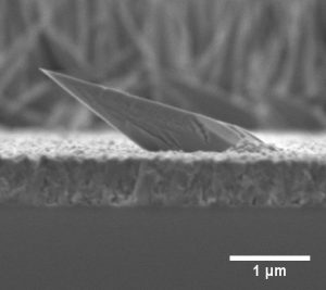
Scanning electron microscopy image of asymmetric gallium phosphide (GaP) nanowires.
A team of scientists presented a route to grow semiconductor nanowires having an asymmetric morphology, different from the traditional cylindrical one. The possibility of producing, in a controlled manner, nanowires with particular formats and without defects, can be exploited in several applications, including the production of more efficient solar cells.
The research was led by scientists from the Brazilian university UNICAMP and the Brazilian Nanotechnology National Laboratory (LNNANO), who reported their findings in a paper in NanoLetters.
The researchers discovered the process while studying the production of nanowires of gallium phosphide (GaP) for optoelectronic applications. The team chose to produce the nanowires by chemical beam epitaxy (CBE), preceded by a thermal treatment (annealing). In this technique, a substrate of a suitable material – in this case gallium arsenide (GaAs) – is placed inside a chamber. Then, chemical compounds in the form of vapor are introduced into the chamber. Some elements of the vapored material deposit over the substrate, layer upon layer, generating films. To promote the growth of nanowires instead of films, metallic nanoparticles (in this case, gold nanoparticles) are placed on the substrate before being exposed to vapor. During exposure, these catalytic nanoparticles cause the material to deposit preferentially underneath them, causing wire-like structures to grow.
While the researchers were analyzing the nanowires they had obtained in the first few months of the work, they found a significant amount of asymmetric nanostructures. “Besides having a particular morphology, we saw that these nanowires had an hexagonal crystal structure (wurtzite) and a very low density of crystallographic defects, which motivated us to study in detail the causes for the formation of this unusual structure,” says Bruno da Silva, PhD student at UNICAMP and corresponding author of the paper.
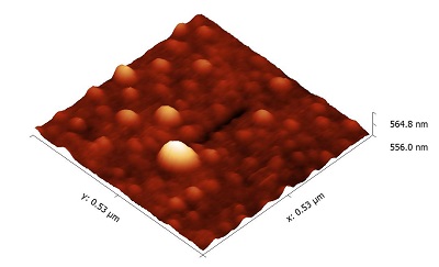
Da Silva and his supervisor Prof. Mônica Cotta then began to raise and test hypotheses for the cause behind the formation of the peculiar structures. After several experiments and analyses, they focused on a phenomenon that caught their attention: in the early stages of the process, the gold nanoparticles spontaneously moved over the substrate. Hence, the duo undertook a systematic work on heating substrates with nanoparticle catalysts, growing nanowires under various conditions, and analyzing the resulting samples through scanning and transmission electron microscopes and atomic force microscopy.
Atomic force microscopy image of a gold nanoparticle on GaAs substrate showing the trail left by its movement.
Da Silva, Prof. Cotta and their collaborators from UNICAMP and LNNano were able to find out why the growth process they used resulted in asymmetric nanowires. The main reason was the movement of the gold nanoparticles, which was thermally activated with the initial annealing. Based on that discovery, the team established a recipe for producing asymmetric semiconductor nanowires in a controlled manner. “Our work was the first to show that the mechanical instability of the nanoparticle catalyst can be used to modify the growth of semiconductor nanowires, in our case, particularly affecting their morphology,” says Bruno da Silva.
The mechanism of the asymmetric nanowires growth presented in the NanoLetters paper can be described as follow. When heated together with the substrate, the nanoparticles begin to crawl and advance through the substrate while consuming the oxide layer that naturally covers the gallium arsenide. Thus, the nanoparticles form asymmetric grooves a few nanometers deep and a few hundred nanometers long. These trails become fertile ground for the growth of the nanowires, since the deposition rate of the vapored material is greater there than in the rest of the substrate, which is covered by the oxide. A pedestal then forms along the grooves and the nanowire grows on top of the pedestal with an asymmetrical format. “We showed that the movement of the particle generates a zone of preferential deposition, and that the combination of this phenomenon with the axial growth “vapor – liquid – solid” leads to the asymmetry in the nanowire,” summarizes da Silva.
Besides describing the formation mechanism of asymmetric nanowires, the work of the Brazilian team generated detailed knowledge about the movement of heated metallic nanoparticles. “We have shown that in addition to temperature, vacuum conditions and surface quality of the substrate are crucial for nanoparticle stability, and that the motion direction is related to the asymmetry of gold dissolution on semiconductor surfaces III-V,” details the doctorate student.
Concerning possible applications, the asymmetry of these nanowires can be explored, for example, in the construction of antireflective layers that reduce the amount of light lost by reflection in solar cells. Another possibility would be to exploit the green emission of these wurtzite gallium phosphide nanowire in lighting devices. Or, why not, to develop an alternative process to electronic litography taking advantage of the gold nanoparticles movement and the trails it forms on the substrate.
The work was funded by Unicamp, the Brazilian federal agencies CNPq and CAPES and the São Paulo Research Foundation (FAPESP).
We look forward to your participation at the XV B-MRS meeting, to be held in September, 25-29, in Campinas, São Paulo. This year the meeting congregates more than 1500 participants, with 2142 accepted abstracts. Fifteen years after the first annual meeting of SBPMat, as it was called then, our figures are impressive, both for the large number of participants and abstracts as well as for the high quality of the scientific contributions, divided in oral and poster presentations. The current edition of the Annual Meeting covers almost all relevant research areas of Materials Science.
The XV B-MRS Annual Meeting is comprised of 20 Symposia, 2 workshops and 2 Tutorials. The program also includes 7 Plenary Lectures from the most prestigious scientists in cutting edge materials science. The Opening Ceremony will be followed by the Memorial Lecture “Joaquim da Costa Ribeiro”; the renowned scientist Aldo Craievich will talk about the relevance and challenges on advanced materials characterization. Furthermore, in this Meeting program, three discussion panels will take place during lunchtime: Research in Germany, Meet the Editors and Materials Research and Innovation. In particular, the latter will discuss research, development and innovation in industry and the role of innovation agencies and startup ventures.
During the Closing Ceremony, the symposium organizers will honor students with the “Bernard Gross Award” for the best poster and best oral presentations of each Symposium. Awards from the European Materials Research Society (E-MRS) and the American Chemical Society (ACS) will be also granted for best posters and oral contributions.
On behalf of Organizing Committee, we would like to thank the Brazil-MRS staff and board, the funding agencies, the symposium organizers and the local committee members, for their commitment and great effort to make this Meeting possible.
We hope we can all enjoy a very hectic Meeting with stimulating exchange of scientific ideas and results, creating new insights and collaborations, to reach even further quality levels in Materials Science research.