Featured paper: Quantum dots with unique rules.

[Paper: Evidence of Band-Edge Hole Levels Inversion in Spherical CuInS2 Quantum Dots. Gabriel Nagamine, Henrique B. Nunciaroni, Hunter McDaniel, Alexander L. Efros, Carlos H. de Brito Cruz, and Lazaro A. Padilha. Nano Lett., 2018, 18 (10), pp 6353–6359. DOI: 10.1021/acs.nanolett.8b02707]

Quantum dots with unique rules

box englishA paper led by Brazilian researchers has revealed surprising news about the rules that determine the energy levels of electrons in quantum dots of copper and indium disulphide (CuInS2,) which stand out in the family of quantum dots for being non-toxic. The work was recently reported in Nano Letters (impact factor of 12.08).

The results of the study, confirmed by experimental and theoretical methods, showed a situation in the structure of energy bands that had never before been observed in other materials.

Diagrama simplicado da estrutura de bandas de um semiconductor. https://en.wikipedia.org/wiki/Valence_and_conduction_bands#/media/File:Semiconductor_band_structure_(lots_of_bands_2).svg
Simple diagram of semiconductor band structure. Credits

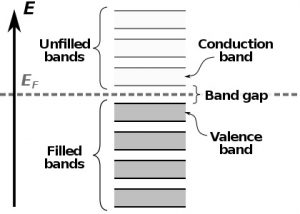
The band structure is a well-established scientific model that shows which energy states or levels the electrons can occupy in a given material. These states of energy are represented as allowed bands (those that the electrons can reach) and forbidden bands (those in which the electrons cannot be found).

In semiconductors, the energy bands that are allowed for an electron and that determine the properties of a material are the valence band and the conduction band. Both are separated by a band gap. For electrons to “jump” from the valence band to the conduction band, transposing the forbidden band in a process called transition, it is necessary they receive extra energy, which can occur when the material absorbs photons. When they lose energy, these electrons can once again occupy their places in the conduction band, and surplus energy can be emitted as photons (light). This light emission from the absorption of photons is known as photoluminescence.

Foto dos estudantes Gabriel Nagamine (na frente) e Henrique Nunciaroni, os dois primeiros autores do paper, trabalhando no laboratório.
Photo of the students Gabriel Nagamine (front) and Henrique Nunciaroni, the first authors of the paper, working in the laboratory.

Researchers at the Gleb Wataghin Institute of Physics at UNICAMP (Campinas, SP, Brazil) discovered that the quantum dots they were studying did not follow the same transition rules as other semiconductor materials and nanomaterials. “Generally, in semiconductors, bulk or nanostructured, the states that form the top of the valence band and the bottom of the conduction band are such that a transition between these states by absorption of a photon is allowed,” contextualizes Lázaro Aurélio Padilha Junior, professor at UNICAMP and corresponding author of the article. “What we showed was that in the studied material (CuInS2 quantum dots), this transition is forbidden by absorbing one photon. The interaction with two photons is required for this transition to occur. As far as we know, this is the first semiconductor system that presents this inversion of states,” says Padilha.

The discovery, besides showing that the norms that govern the electron states in semiconductors are not valid for all the materials, can influence the applications of the quantum dots studied. According to Padilha, the conditions discovered favor the simultaneous emission of two photons in the material when the electrons return to the conduction band. “This could be attractive to lasers systems that emit light in two distinct colors at the same time, and with color adjustment over a wide spectral range,” says the professor. In addition, adds Gabriel Nagamine, the first author of the article, understanding the structure of material bands can improve the performance of existing applications such as luminescent solar concentrators – a technology that can be used both to generate electricity from sunlight and to increase the production of food in greenhouses. “All these applications come from the unique characteristics of the electronic bands of these materials,” says Nagamine.

History of a theoretically announced experimental result

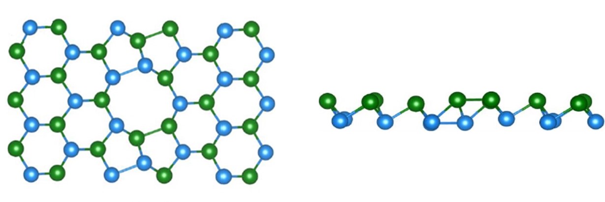
The history of this discovery goes back to 2015, when Professor Padilha, who has worked with quantum dots since 2010, his master’s student Gabriel Nagamine and other members of the research group decided to devote their efforts in studying the quantum dots of CuInS2. “This material caught our attention because it did not have heavy metals in its composition, which made it interesting for applications in biology and medicine, such as fluorescent biological markers,” says Padilha. In fact, quantum dots, which were discovered in the 1980s and are now present in products such as TV screens, present very interesting properties to be used in the detection of diseases and other applications in the health area, but almost all of them are toxic due to their chemical composition.

Esta figura mostra o espectro de absorção de dois fótons (pontos amarelos) e o espectro de absorção de um fóton (línea azul) em pontos quânticos de CuInS2 esféricos. As setas indicam os picos de absorção de dois fótons (setas amarelas) e de um fóton (seta azul). No canto superior esquerdo, há uma imagem de microscopia eletrônica de transmissão mostrando um dos pontos quânticos.
Two-photon (yellow dots) and one-photon (blue line) absortion spectra in spherical CuInS2 quantum dots. Arrows: absortion peaks of two photons (yellow) and one photon (blue). In the upper left corner, TEM image showing one of the quantum dots.

The UNICAMP team then collaborated with the company UbiQD, located in Los Álamos (USA) and specialized in the production of quantum dots, and which provided samples of spherical and pyramidal quantum dots. The characterization of the samples was performed partly in the company and also in the National Nanotechnology Laboratory (LNNano) of CNPEM, in the city of Campinas (SP, Brazil).

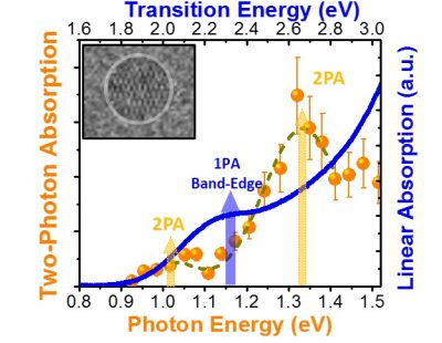
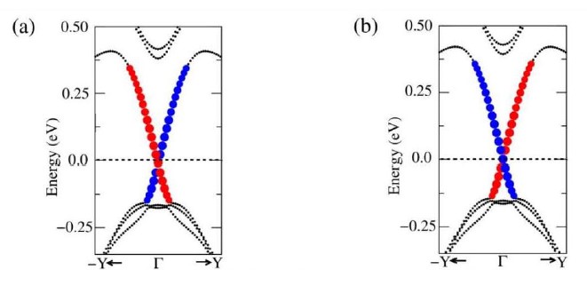
Initially, Padilha and his team set out to investigate how strong the absorption of two photons was in the chosen material, since this optical process allows to make three-dimensional images of the material, which can be very useful in its characterization and also in its application in several areas. To do this, in early 2016, the team performed the main experiments of the work at UNICAMP using a spectroscopy technique that allows detecting light emission from the absorption of two photons. “The first measurements revealed an absorption peak of two photons at smaller energies than those of linear absorption – a fact never previously observed experimentally,” Padilha says. “We believed it was a problem in our laser source and we repeated the experiment, achieving the same results,” he adds. These results, which are shown in the figure to the side, have arisen from the experiments performed with spherical quantum dots. In the pyramid-shaped quantum dot samples, the predominance of of two-photon absorption was not observed.

In May of the same year Padilha met with Dr. Alexander Efros (Naval Research Laboratory, USA) at a conference in South Korea. “He, who is one of the most respected theorists working on the electronic structure of semiconductor quantum dots, mentioned that he had made calculations that predicted a reversal in parity of states in these nanomaterials. We immediately noticed that I had proven his theory, “says Prof. Padilha. After that, they began working together and trying to understand other aspects of the problem, until they submitted the article to Nano Letters. The paper was accepted in less than two months.

The research that originated the paper is part of Gabriel Nagamine’s master’s thesis, defended in 2017 at UNICAMP, and received financial support from Brazilian research agencies (FAPESP and federal CNPq), the student support service (SAE) of UNICAMP and the Office of Naval Research (USA).

ACS Publications will award prizes to the best student contributions of the XVI B-MRS Meeting.

Until August 14, undergratudate and graduate students who are authors of accepted abstracts can apply for the student awards of the XVI B-MRS Meeting. In addition to the traditional “Bernhard Gross Award” from the Brazilian Materials Research Society, this edition of the event will feature awards from the publisher of the American Chemical Society (ACS Publications), responsible for a number of very prestigious peer-reviewed scientific journals in the materials field.

The Bernhard Gross Award was established by SBPMat in honor of the pioneer of Brazilian materials research Bernhard Gross, and it distinguish the best works (up to 1 oral and 1 poster) from each symposium.

Among the winners of the Bernhard Gross Award, the three best posters and the three best oral presentations will receive the “ACS Publications Best Poster Prize” and the “ACS Publications Best Oral Presentation Prize” respectively. The prizes will consist of US $ 500 for each winning work, in addition to the certificate. The ACS awards will be sponsored by the following ACS’s journals: ACS Applied Materials & Interfaces, ACS Nano, Nano Letters, Chemistry of Materials, JACS and ACS Omega.

In order to compete for the prizes, students have to submit through the website of the event, an extended abstract, elaborated according to the template that is available in the instructions for authors.

The papers will be evaluated considering the quality of the extended abstracts and presentations, as well as the scientific contribution of the research work.

The Student Awards Ceremony will take place at the closing of the XVI B-MRS Meeting, on September 14. Prizes will only be given if the winner students are present at the ceremony.

Seis periódicos da ACS patrocinarão os prêmios para  as melhores contribuições de estudantes.
                                       Six ACS journals will sponsor the prizes for the best student contributions.

Featured paper: Isolating nanoribbons with conducting regions.

[Paper: Topologically Protected Metallic States Induced by a One-Dimensional Extended Defect in the Bulk of a 2D Topological Insulator. Erika N. Lima, Tome M. Schmidt, and Ricardo W. Nunes. Nano Lett., 2016, 16 (7), pp 4025–4031. DOI: 10.1021/acs.nanolett.6b00521]

Isolating nanoribbons with conducting regions

A research carried out in Brazil made an important contribution to the study of topological insulators, a class of materials that was theoretically predicted in 2005 and experimentally confirmed in 2007. The study was reported in an article recently published  in Nano Letters (impact factor: 13.779).

A unique property of Topological insulators is that they behave as insulators on the inside and as conductors on its surface or edge. According to Ricardo Wagner Nunes, professor at the Federal University of Minas Gerais (UFMG) and corresponding author of the article, “non-topological insulators may also have conductive surfaces, but in the case of topological insulators, conduction of charge and spin on the surface is robust, as it is “protected” by time reversal symmetry”.

In the article in Nano Letters, Professor Nunes and colleagues, Erika Lima, of the Federal University of Mato Grosso (UFMT) – Rondonópolis campus, and Tome Schmidt, of the Federal University of Uberlândia (UFU), reported their work on a two-dimensional topological insulator, a bismuth nanoribbon of only two layers of bismuth atoms (one-atom thick), superimposed and bonded. Using computational methods, the scientists showed that the interior of the bismuth nanoribbon, instead of being fully insulating, may have conductive states (also called metallic states) generated from a particular type of irregularity in the atomic structure of the material, known as 558 extended defect.

Representation of bismuth bilayer nanoribbon with the defect 558, top view (left) and side view (right). The green balls represent the atoms of the top layer of the material and the blue balls, the atoms of the lower layer. In the center of the left figure, the defect is clearly seen: pentagons and an octagon stop the repetition of the hexagons.


“In our work, we show that a linear defect within a two-dimensional topological insulator can generate one-dimensional electronic quantum states that conduct spin and charge within the material”, say the authors.

This conclusion was supported through calculations performed on supercomputers, simulating what would happen to the electrons in quantum states, in the material, in the presence of defects. “We used first-principles Density Functional Theory calculations”, specify the authors, who relate that the computer simulation of defects in bismuth nanostructures required approximately 400 hours of computer simulations on supercomputers in the Department of Physics – UFMG and at the National Center for High Performance Computing in São Paulo (Cenapad) – UNICAMP.

A figura mostra a curva de dispersão dos estados topológicos metálicos, localizados no defeito 558, marcados em azul e vermelho.
The figure shows, marked in blue and red, the dispersion curve of the metal topological states located in the defect 558.

In the article, the authors also propose the existence of pentaoctite, a new two-dimensional topological insulator. This material, which has not been synthesized yet, is a bismuth bilayer with a crystal lattice formed by atoms arranged in pentagons and octagons. As stated by the authors, “In our calculations we show that this new “phase” of the two-dimensional bismuth has low formation energy, which opens the possibility to be synthesized in the laboratory”.

According to the authors, the work reported in Nano Letters raises several issues in the scope of fundamental research, such as the influence of magnetic and non-magnetic impurities on the spin and charge transport in the proposed topological states, and the connection between the network symmetries and nature of the topological edge states on pentaoctite. “From the point of view of applications, it would be interesting if our work could motivate experimental studies of two-dimensional topological insulators based on bismuth and other materials, enabling theoretical and experimental collaboration on this issue”, comment the authors, leaving an open invitation to experimental research groups.

The origin of this research work

“The work originated by combining my interest in extended topological defects in two-dimensional and three-dimensional materials, with the experience of Professor Tome Mauro Schmidt (UFU) and Erika Lima, his doctoral student in the subject of topological insulators”, states Nunes.

In 2012, Nunes and collaborators published an article in Nano Letters on magnetic states (non topological) generated by linear extended defects in a monolayer of graphene. Later, in a conversation with Schmidt, a collaboration was decided in order to investigate if an extended defect with the same morphology would lead to the formation of topological states in a bidimensional topological insulator made of bismuth.

In her post-doctorate in the group of Professor Nunes, in 2015, Erika Lima performed all computer calculations. The three researchers, who are the authors of the article, interpreted the results and wrote the paper.

The research that led to the article received funding from Brazilian agencies CAPES, CNPq, FAPEMIG and from the National Institute of Science and Technology on Carbon Nanomaterials.

autores
Photos of the authors. From left to right, Erika Lima, currently a professor at UFMT, Tome Schmidt, professor at UFU, and Ricardo Nunes, professor at UFMG.

Featured paper. Nanotubes that coil to the sound of music: tango or chorinho.

[Paper: Defect-Free Carbon Nanotube Coils. Nitzan Shadmi, Anna Kremen, Yiftach Frenkel, Zachary J. Lapin, Leonardo D. Machado, Sergio B. Legoas, Ora Bitton, Katya Rechav, Ronit Popovitz-Biro, Douglas S. Galvão, Ado Jorio, Lukas Novotny, Beena Kalisky, and Ernesto Joselevich. Nano Lett., 2016, 16 (4), pp 2152–2158. DOI: 10.1021/acs.nanolett.5b03417]

Nanotubes that coil to the sound of music: tango or chorinho

Among the many applications foreseen for carbon nanotubes, there are some nanoelectronic devices that make use of the excellent ability to conduct electricity, through the tiny graphene tubes. For the good performance of nanotubes in some of these applications, the most suitable are the coil configurations, formed by a single nanotube with its two ends free to make contact with other components within a device. Additionally, to not lose conductivity, the nanotube coil should have relatively low density of structural defects.

In practice however, it is not easy for a human being to achieve 1 nm diameter tubes to twist into spiral loops without generating imperfections and leaving their tips separate from the bundle.

Cover of Nano Letters. Representation of a coil formed by a single coiled carbon nanotube. Top right, the insert highlights, through a scanning electron microscopy image, the cross section of a real coil obtained by the team of scientists.

In an article published in the prestigious Nano Letters journal, highlighted in the cover of the April issue of this year, a team of 14 scientists reported the formation of defect-free nanotube coils with free ends, from a spontaneous coiling mechanism of single-wall carbon nanotubes. The study was led by researchers from the Weizmann Institute of Science (Israel) with the participation of four scientists from Brazilian universities (State University of Campinas, Unicamp; Federal University of Minas Gerais, UFMG, and Federal University of Roraima), from ETH Zürich (Switzerland) and from the Bar-Ilan University (Israel).

The team placed iron nanoparticles on silicon dioxide substrates and added a carbon-containing gas – a combination known to promote the growth of long single-wall nanotubes, which can reach more than 100 microns in height. The nanotubes grow perpendicular to the substrate like a forest of trees.

Under these conditions, the scientists created several carbon nanotubes samples, and some were spontaneously coil shaped. The authors analyzed the nanotube coils using SEM, TEM and AFM, obtaining information such as diameter, height and number of coil turns. Using the Raman spectroscopy technique, the authors continued investigating the nanotube coils and found a very low concentration of structural defects and also found that the diameter and chirality of the nanotubes were the same throughout the coil. The Raman spectroscopy analyses were partially carried out at the UFMG by Brazilian Professor Ado Jorio.

To understand the coil formation mechanism, the team used atomistic molecular dynamics simulations, used to depict the physical movements of atoms and molecules. These simulations were headed by Professor Douglas Soares Galvão (Institute of Physics Gleb Wataghin – Unicamp) and carried out by the postdoctoral researcher Leonardo Dantas Machado, former student of Galvão, and by Professor Sergio Benites Legoas (Federal University of Roraima), ex-postdoctoral grant holder in Galvão’s group. At IFGW – Unicamp, Prof. Galvão heads a research group specialized in simulation and computer modeling of nanostructured materials, particularly involving nanowires and nanotubes, and often collaborating with experimental groups from different countries. Through the simulations, the group is able to study, understand and predict phenomena that are sometimes not directly viewed or accessed experimentally in the time scale in which they occur.

Generally speaking, the simulations showed that after growing vertically, the nanotubes that had formed coils began to deposit on the substrate from the bottom up, forming the first turn as a result of their interaction with the carbon gas flow and with the substrate. After this first step, the nanotubes continued to spontaneously and steadily be deposited in a coil-like shape, completing up to 74 turns.

The team also investigated the performance of the coils as inductors (coiled devices that generate magnetic fields when an electrical current passes through, also known as electromagnetic coils) – a nanotube application that had not been studied until now. In the Nano Letters article the nanotube coils showed that despite being highly conductive, they are not yet ready to be used as efficient inductors. However, in the article the analysis of its electrical and magnetic behavior presented new and valuable information which can be used to develop inductive devices from nanotubes.

Cover of Physical Review Letters highlighted in 2013 another article of the international team of scientists, led by Galvão, on carbon nanotube coils.

According to Professor Galvão, the paper published in Nano Letters is a continuation of a previous project on carbon nanotube serpentines that involved his group, the group of Israel, led by Ernesto Joselevich, and Professor Ado Jorio (UFMG). This first study also produced an article featured on the cover of a prestigious journal, the Physical Review Letters (Dynamics of the Formation of Carbon Nanotube Serpentines, L. D. Machado, S. B. Legoas, J. S. Soares, N. Shadmi, A. Jorio, E. Joselevich, and D. S. Galvão, Phys. Rev. Lett. 110, 105502 – Published 8 March 2013).

Galvão recounts that the collaboration between the Brazilians and the Israel group began at a conference in Spain, where he attended a presentation by Joselevich on serpentine-shaped carbon nanotubes. “I believed it was a very interesting problem”, says Galvão. Coincidentally, the two scientists met again in a Brazilian event of condensed matter physics and had lunch together with Ado Jorio. That is when their collaboration began. “From the point of view of simulation, it was a very challenging and difficult project (in addition to specifically developing new protocols for the problem, the simulations involve millions of atoms), but Leonardo and Legoas were able to solve this”, says Galvão.

In addition to being consistent from the scientific point of view, the simulations were interesting from an aesthetic point of view. In this regard, Professor Galvão shares an anecdote. “Joselevich, who is Argentine by birth, knows Brazil and the Brazilian culture quite well. The first time he saw the serpentine simulations, he remembered the melody of “Brasileirinho” (a famous piece of chorinho music). We prepared some video versions incorporating the Brasileirinho as the soundtrack in his honor, jesting with the Brazil-Argentina rivalry, and others with tangos. The Brasileirinho wins, of course”, says the professor jokingly.

Two videos of nanotube dancing and forming coils can be accessed free of charge in the supporting info published with the paper in Nano Letters: http://pubs.acs.org/doi/abs/10.1021/acs.nanolett.5b03417

Featured paper: Vibrations of manipulated nanotubes.

[Paper: Strain Discontinuity, Avalanche, and Memory in Carbon Nanotube Serpentine Systems. Muessnich, Lucas C. P. A. M.; Chacham, Helio; Soares, Jaqueline S.; Neto, Newton M.; Shadmi, Nitzan; Joselevich, Ernesto; Cancado, Luiz Gustavo; Jorio, Ado. Nano Lett. 2015, 15 (9), pp 5899–5904. DOI: 10.1021/acs.nanolett.5b01982]

Vibrations of manipulated nanotubes.

Scientists from Brazilian institutions, in collaboration with researchers from Israel, “manipulated” carbon nanotubes of 1 nm diameter deposited on quartz surfaces and analyzed strain and displacements produced by this nanointervention. The team identified some behavior patterns in the nanotubes – quartz system and formulated a mathematical model applicable to systems formed by one- and two-dimensional materials over various substrates. The results of the study were recently published in Nano Letters.

To perform the experiments, the Brazilian investigators used samples idealized and produced in the Weizmann Institute of Science (Israel), in which the nanotubes are serpentine-shaped (composed of parallel segments connected together by U-shaped curves).These samples offered a desirable complexity, fostered by both the nanotubes format and the anisotropic character of quartz, which makes adhesion of nanotubes to the substrate not the same at all points.

In order to “manipulate” the system, the researchers used the tip of an atomic force microscope (AFM) built in the laboratory, which allows to change the position of nanometric particles and even of atoms, and to measure in situ the optical spectrum of nanostructures. In each sample, the tip touched a point of the quartz substrate and pushed toward the nanotube, and then proceeded to the optical analysis.

Before and after nanomanipulation, the scientists analyzed a number of points in the nanotube using the technique of Raman spectroscopy, which provides information about the frequency in which the atoms vibrate in the area being studied. More specifically, researchers focused on the frequency of the “G band”, which is used to infer the strain measurements of a considered point, since changes in the frequency of the “G band” are proportional to changes in strain.

Thus, scientists were able to identify and analyze different behavior of the nanotubes after nanomanipulation; for example, the detachment of the substrate and the intense displacement of a full stretch of the nanotube that had received two manipulations at the same point.

In addition to performing the experimental work, the authors of the article in Nano Letters managed to condense the complexity of behaviors they observed in a mathematical model (an equation) capable of explaining them theoretically and predicting these phenomena in similar systems. “The paper proposes a relatively simple model to describe complex effects of nanostructures adhesion in support media,” says Ado Jório, professor in the Department of Physics of the Federal University of Minas Gerais (UFMG) signing the letter as corresponding author.

The research that led to the Nano Letters article was developed within the master’s, doctoral and postdoctoral work of three authors of the letter, in the context of the Brazilian Network for Research and Instrumentation in Optical Nano-Spectroscopy, a project funded by the National Council for Scientific and Technological Development (CNPq) and coordinated by Ado Jório. “This is the result of a broad scientific instrumentation project, which aims at reaching the level of manipulating nanostructures and measuring, accurately, the effect of this process at the nanoscale,” says Jório.

The figure shows one of the 34 serpentine-shaped nanotubes on crystalline quartz substrate studied by the authors of the article. To the left of the reader is the nanotube before manipulation. To the right, following the sequence, the same nanotube after the intervention, with the consequent evident strain. The central segment of the nanotube, where the nanomanipulation occurred, was colorized, the gray scale indicating the frequency of the G band in that place. Finally, farther to the right, the chart displays the frequency of G band measured by Raman spectroscopy in successive points of this nanotube (graphical representation of gray hues): the black circles refer to non-manipulated nanotube and the gray colored circles, to the manipulated ones.