Featured paper: Disclosing structural disorder in nanomaterials.

[Paper: Decreasing Nanocrystal Structural Disorder by Ligand Exchange: An Experimental and Theoretical Analysis. Gabriel R. Schleder, Gustavo M. Azevedo, Içamira C. Nogueira, Querem H. F. Rebelo, Jefferson Bettini, Adalberto Fazzio, Edson R. Leite. J. Phys. Chem. Lett. 2019 10 1471-1476. https://doi.org/10.1021/acs.jpclett.9b00439]

Disclosing structural disorder in nanomaterials

It is known that it is very important to know and control the structure of a material (how its atoms are arranged in three-dimensional space) as it is largely responsible for the properties of the material and therefore for its applications. For example: regions of disorder in crystalline materials (whose atoms, ideally, are ordered in regular patterns) change some expected behaviors for these materials. Unfortunately, knowing the structure of some materials in detail can be a difficult task – particularly when it comes to nanomaterials.

Concentrating various skills and experimental and theoretical resources, a Brazilian team developed a method to establish the degree and location of disorder in the structure of crystalline and non-crystalline nanomaterials, interfaces and surfaces. The method, which is based on the combination of an experimental technique (transmission electron microscopy), a data analysis method (pair distribution function) and computational simulations, is already available to the scientific community at the Brazilian National Nanotechnology Laboratory (LNNano), and should help develop better performing materials.

In addition to developing the technique, the team applied it in the study of structural disorder in nanocrystals, which are basic elements of nanotechnology and are used for example, in solar cells and electronic devices. Although by definition they have ordered structures, these crystals of nanometric dimension can exhibit, in practice, regions with structural disorder.

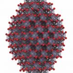
In order to carry out the study, the scientists produced faceted nanocrystals of about 3.2 nm in diameter, formed by a core of zirconium dioxide (ZrO2), inorganic material, and a shell made up of organic substances known as ligands, whose atoms form chemical bonds with atoms that are on the surface of the inorganic nucleus. Ligands have the important role of stabilizing the nanocrystals, thus preventing them from aggregating.

The team produced a first series of nanoparticles with ligands containing an aromatic ring and analyzed it using the developed method. The samples were then subjected to a process known as ligand exchange in which chemical reactions occur in the material in the presence of a solvent at a temperature above its boiling point. In these reactions, some connections break down and new connections occur. As a result of the ligand exchange, the team was able to produce nanoparticles with shells containing oleic acid, which were also analyzed using the developed method.

This figure refers to a nanocrystal of ZrO2 before and after the ligand exchange. The figure includes high-resolution images of transmission electron microscopy, structural models and PDF patterns obtained by the developed method.

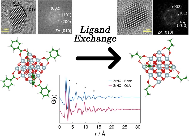
The scientists concluded that, unlike the ideal nanocrystal of zirconium dioxide, the two types of nanocrystals analyzed had a degree of structural disorder located on the surface of the nucleus.  In addition, in the second group of nanoparticles, the disorder was significantly lower. The researchers interpreted this reduction as a result of the high temperature of the ligand exchange process, which altered the tensions of the network of atoms.

“In our work, we were able to directly assess the degree and location of disorder in the nanocrystals, which until then was not technically feasible,” says Gabriel Schleder, PhD candidate in the Graduate Program in Nanosciences and Advanced Materials of the Brazilian Federal University of the ABC (UFABC).

By better understanding structural disorder and its causes, the researchers were able to point out a way to control it. “Any property that significantly depends on surface-located structural disorder could be in principle controlled by this kind of ligand exchange process,” says Schleder. “Mechanical properties, photoluminescence, electronic transport and catalytic properties are some of them,” he adds.

The research was reported in a recently published article in The Journal of Physical Chemistry Letters (impact factor = 8,709).

Overcoming the challenge through collaborations

The initial idea of the study appeared in a meeting held at the end of 2017 at the National Center for Research in Energy and Materials (CNPEM), located in the city of Campinas, São Paulo. At the meeting, a group of reserachers discussed the implementation in Sirius (the next Brazilian synchrotron light source) of a technique that allows locally analyzing structural issues such as disorder and defects, called pair distribution function (PDF). The technique describes the distances between pairs of atoms by means of a mathematical function. To apply it, the specialist generally uses the results of X-ray diffraction measurements – an experimental technique that provides information about the structure of materials. However, in order to implement the analysis by PDF, the X-ray beam focused on the sample must be of very high energy – higher than that provided by the current Brazilian synchrotron light source.

During the meeting at CNPEM, Professor Gustavo de Medeiros Azevedo, researcher at the National Laboratory of Synchrotron Light (LNLS), and Professor Edson Leite, LNNano’s scientific director, decided to begin applying PDF using electron diffraction results, a specialty of LNNano’s researcher Jefferson Bettini. The electron beams would be generated by the transmission electron microscope (TEM) of LNNano. In fact, this instrument allows the control of the electron beam so that it focuses a small area of the sample, allowing the desired local analysis of the structure. Besides that, when switching from the “diffraction mode” to the “image mode”, the microscope would made possible to choose precisely the area of the sample to be analyzed.

Simulation of an ideal ZrO2 nanocrystal.

The development team also involved professors Içamira Costa Nogueira, from the Federal University of Amazonas (UFAM) and Querem Hapuque Felix Rebelo, from the Federal University of the West of Pará (UFOPA), who contributed with the synthesis of nanocrystals that would be studied and with the development of the analysis methodology.

During the development of the technique, another challenge had to be faced. To interpret the PDF results, it would be necessary to have a simulation of an ideal nanocrystal – a nanocrystal model without structural disorganization that could be used as a reference.

New skills were then incorporated into the team, which was then joined by Professor Adalberto Fazzio, director general of LNNano and leader of a UFABC research group dedicated to computational techniques applied to materials, and his doctoral student Gabriel Schleder. Based on the Density Functional Theory (DFT), a computational modeling method in the field of Quantum Physics, the researchers were able to simulate the ideal nanocrystal that served as the analysis model.

“Something very positive we perceived is that the main results arose from the process of interaction, discussion and exchange of information mainly between theory/computational simulation and experiments. Without this, we certainly would not have good final conclusions,” says Schleder.

The authors of the paper. From the left: Gabriel R. Schleder, Gustavo M. Azevedo, Içamira C. Nogueira, Querem H. F. Rebelo, Jefferson Bettini, Adalberto Fazzio and Edson R. Leite.

Members of B-MRS are authors of a new book on Density Functional Theory.

Prof Sérgio Ricardo de Lázaro (left) and Luis Henrique da Silveira Lacerda.

The members of B-MRS Sérgio Ricardo de Lázaro (UEPG professor) and Luis Henrique da Silveira Lacerda (PhD student at UEL/UEPG/UNICENTRO) are the authors of the book “Teoria do Funcional da Densidade e Propriedades dos Materiais“, published by the Brazilian publishing house CRV. The book is co-authored by Renan Augusto Pontes Ribeiro, also a doctoral student of the program. The Density Functional Theory (DFT) is based on Quantum Mechanics and was applied in the area of Materials Chemistry.

More information about the book: https://editoracrv.com.br/produtos/detalhes/33536-crv

Featured paper: Isolating nanoribbons with conducting regions.

[Paper: Topologically Protected Metallic States Induced by a One-Dimensional Extended Defect in the Bulk of a 2D Topological Insulator. Erika N. Lima, Tome M. Schmidt, and Ricardo W. Nunes. Nano Lett., 2016, 16 (7), pp 4025–4031. DOI: 10.1021/acs.nanolett.6b00521]

Isolating nanoribbons with conducting regions

A research carried out in Brazil made an important contribution to the study of topological insulators, a class of materials that was theoretically predicted in 2005 and experimentally confirmed in 2007. The study was reported in an article recently published  in Nano Letters (impact factor: 13.779).

A unique property of Topological insulators is that they behave as insulators on the inside and as conductors on its surface or edge. According to Ricardo Wagner Nunes, professor at the Federal University of Minas Gerais (UFMG) and corresponding author of the article, “non-topological insulators may also have conductive surfaces, but in the case of topological insulators, conduction of charge and spin on the surface is robust, as it is “protected” by time reversal symmetry”.

In the article in Nano Letters, Professor Nunes and colleagues, Erika Lima, of the Federal University of Mato Grosso (UFMT) – Rondonópolis campus, and Tome Schmidt, of the Federal University of Uberlândia (UFU), reported their work on a two-dimensional topological insulator, a bismuth nanoribbon of only two layers of bismuth atoms (one-atom thick), superimposed and bonded. Using computational methods, the scientists showed that the interior of the bismuth nanoribbon, instead of being fully insulating, may have conductive states (also called metallic states) generated from a particular type of irregularity in the atomic structure of the material, known as 558 extended defect.

Representation of bismuth bilayer nanoribbon with the defect 558, top view (left) and side view (right). The green balls represent the atoms of the top layer of the material and the blue balls, the atoms of the lower layer. In the center of the left figure, the defect is clearly seen: pentagons and an octagon stop the repetition of the hexagons.


“In our work, we show that a linear defect within a two-dimensional topological insulator can generate one-dimensional electronic quantum states that conduct spin and charge within the material”, say the authors.

This conclusion was supported through calculations performed on supercomputers, simulating what would happen to the electrons in quantum states, in the material, in the presence of defects. “We used first-principles Density Functional Theory calculations”, specify the authors, who relate that the computer simulation of defects in bismuth nanostructures required approximately 400 hours of computer simulations on supercomputers in the Department of Physics – UFMG and at the National Center for High Performance Computing in São Paulo (Cenapad) – UNICAMP.

A figura mostra a curva de dispersão dos estados topológicos metálicos, localizados no defeito 558, marcados em azul e vermelho.
The figure shows, marked in blue and red, the dispersion curve of the metal topological states located in the defect 558.

In the article, the authors also propose the existence of pentaoctite, a new two-dimensional topological insulator. This material, which has not been synthesized yet, is a bismuth bilayer with a crystal lattice formed by atoms arranged in pentagons and octagons. As stated by the authors, “In our calculations we show that this new “phase” of the two-dimensional bismuth has low formation energy, which opens the possibility to be synthesized in the laboratory”.

According to the authors, the work reported in Nano Letters raises several issues in the scope of fundamental research, such as the influence of magnetic and non-magnetic impurities on the spin and charge transport in the proposed topological states, and the connection between the network symmetries and nature of the topological edge states on pentaoctite. “From the point of view of applications, it would be interesting if our work could motivate experimental studies of two-dimensional topological insulators based on bismuth and other materials, enabling theoretical and experimental collaboration on this issue”, comment the authors, leaving an open invitation to experimental research groups.

The origin of this research work

“The work originated by combining my interest in extended topological defects in two-dimensional and three-dimensional materials, with the experience of Professor Tome Mauro Schmidt (UFU) and Erika Lima, his doctoral student in the subject of topological insulators”, states Nunes.

In 2012, Nunes and collaborators published an article in Nano Letters on magnetic states (non topological) generated by linear extended defects in a monolayer of graphene. Later, in a conversation with Schmidt, a collaboration was decided in order to investigate if an extended defect with the same morphology would lead to the formation of topological states in a bidimensional topological insulator made of bismuth.

In her post-doctorate in the group of Professor Nunes, in 2015, Erika Lima performed all computer calculations. The three researchers, who are the authors of the article, interpreted the results and wrote the paper.

The research that led to the article received funding from Brazilian agencies CAPES, CNPq, FAPEMIG and from the National Institute of Science and Technology on Carbon Nanomaterials.

autores
Photos of the authors. From left to right, Erika Lima, currently a professor at UFMT, Tome Schmidt, professor at UFU, and Ricardo Nunes, professor at UFMG.