[Paper: Oxide-cladding aluminum nitride photonic crystal slab: Design and investigation of material dispersion and fabrication induced disorder. Melo, EG; Carvalho, DO; Ferlauto, AS; Alvarado, MA; Carreno, MNP; Alayo, MI. Journal of Applied Physics 119, 023107 (2016). DOI: 10.1063/1.4939773.]
Designing structures to manipulate light
Photonic crystals are nanostructures capable of manipulating visible light and other forms of electromagnetic radiation by organizing its structure in periodic patterns.
In addition to the natural materials with these characteristics, such as opal, photonic crystals are man-made and are generally classified as metamaterials. Its characteristics (shape, size and composition) are designed to control light waves. Through nanofabrication processes these become tangible structures and are used in many “nanophotonic” devices. Nevertheless, producing these structures is by no means a simple task.

With a study based on computer simulations, a team of Brazilian scientists headed by researchers from the Polytechnic School of the University of São Paulo (EPUSP) presented scientific contributions that can be used to improve the production of photonic crystals to enhance their performance of manipulating light. According to Emerson Melo, the first author of a paper on the study that was recently published in the prestigious Journal of Applied Physics (JAP) “the work presents a detailed analysis of the effects caused by nanofabrication processes on the optical properties of planar photonic crystals produced on silicon dioxide-cladding aluminum nitride”.
“The idea emerged from the opportunity of combining the excellent optical and physical characteristics of aluminum nitride (AlN), such as transparency over a wide wavelength range (from the near infrared to the ultraviolet range), its non-linear effects, great stability and temperature variations, with the advantages provided by photonic crystals, such as the construction of high-efficiency waveguides, curves and resonant cavities in nanoscale dimensions, in addition to the various optical effects of photonic crystals, such as very low group velocity and low-intensity nonlinear effects of the materials”, adds Emerson, who is a doctoral student in Microelectronics – Photonics in EPUSP, within the Group of New materials and Devices of the Microelectronics Laboratory of the Department of Electronic Systems Engineering. Emerson`s doctoral research, whose advisor is Professor Marco Isaías Alayo Chávez, enquires into the study, production and characterization of nanophotonic devices such as waveguides, resonant cavities, optical modulators and switches in aluminum nitride photonic crystals.
The study that resulted in the paper published in the JAP began with an experimental stage. Thin films of aluminum nitride and silicon dioxide (SiO2) were manufactured by the EPUSP group, and with the research collaboration from UFMG and UNESP they were analyzed by the Variable Angle Spectroscopic Ellipsometry (VASE) technique to determine the dielectric functions, which was later used as the theoretical research data.

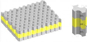
Then, the EPUSP group designed a photonic crystal, ideal in terms of performance and manufacturing possibilities, consisting of a layer of aluminum nitride between two silicon dioxide layers, with round holes arranged in a repeating pattern along the “sandwich” material. Using analytical and numerical methods, the USP researchers simulated some of the “side effects” of the photonic crystal manufacturing processes of this type (e.g., variations of size and location of holes) and theoretically analyzed how these imperfections affect the performance of the photonic crystal.
The theoretical research of Emerson and the other researchers of EPUSP focused on the imperfections generated in the two main stages of the nanofabrication process normally used in photonic crystals such as the one studied: electron-beam lithography and plasma-assisted dry etching. “The results presented allow to assess that the electron-beam lithography process has greater effect on the performance of devices that explore the dispersion of electromagnetic radiation through the photonic crystal, such as prisms, optical switches and modulators”, says Emerson. “However, the quality of the dry etching process has a more profound impact on the characteristics of devices into which linear or exact defects are introduced in the periodic network of the photonic crystal to insert harmonic modes within the photonic band gap. In this case, the dry etching has to be extremely well controlled for manufacturing the devices where waveguides and resonant cavities are among its main elements”.
In addition to making headway in understanding the role of nanofabrication processes of photonic crystals in the performance of nanophotonic devices, the authors of the paper were able to define a method to design planar photonic crystals with core and cover in thin film dielectric materials. “The methodology includes determining the dielectric function of the material by the spectroscopic ellipsometry technique to analyze the dispersion effects of the materials, determining the geometrical parameters that maximize the photonic band gap and the analysis of the impacts caused by deviations introduced in the manufacturing process”, explains Emerson.
The research received financial support from the National Council for Scientific and Technological Development (CNPq) and from the Financier of Studies and Projects (Finep).
The authors of the article. From left to right, at the laboratory:.
