Featured paper: Controlling the electronic properties of graphene on silicon carbide.

[Paper: Graphene on the oxidized SiC surface and the impact of the metal intercalation. J.E.Padilha, R.B.Pontes, F. Crasto de Lima, R. Kagimura, R. H. Miwa. Carbon, Volume 145, April 2019, Pages 603-613.]

Controlling the electronic properties of graphene on silicon carbide

A Brazilian scientific team performed a study based on supercomputer simulations that reveals a way to overcome the challenge of controlling the electronic properties of graphene. Solutions to this challenge can make a difference in the development of two-dimensional electronic devices – a dimension in which graphene, the one-atom thick network of carbon atoms, stands out for its properties.

In fact, graphene is an extremely tough, lightweight, flexible and transparent material. It is also an excellent conductor of heat and electricity. However, it is still difficult to control the concentration and flow of electric charges in graphene, which limits its use in electronics.

Solutions have been proposed to overcome this technological limitation of graphene. Some of them are based on the insertion of small amounts of metallic atoms that modulate the electronic properties of the material without impairing the other characteristics. The method is similar to the doping of silicon, practiced routinely in the manufacture of semiconductors for the electronics industry.

Representation of the studied system: graphene sheet on substrate of oxidized silicon carbide with layer of intercalated metallic atoms (in this case, gold).

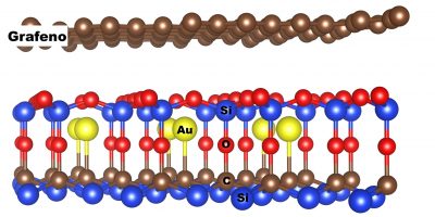
In the study that was recently reported in the scientific journal Carbon (impact factor 7,466), the Brazilian team investigated the structure and electronic properties of a graphene sheet on a silicon carbide (SiC) substrate – material often used to deposit or grow graphene. In this system, graphene remains attached to the substrate without chemical bonds, by means of distance-dependent weak attraction forces, called Van der Waals forces.

Given that in the production of graphene the presence of oxygen usually oxidizes the surface of the silicon carbide, the Brazilian scientists included in the simulations a layer of silicon oxide between the graphene and the substrate. Finally, in order to understand in detail the effect of the insertion of metallic atoms into this type of materials, the scientists added to the simulated system a layer of gold or aluminum atoms embedded in the oxide layer (in this case, Si2O5) in the interface region with graphene.

The researchers verified that the presence of the metallic layer modulates the concentration of the positive (so-called holes) and negative (the electrons) charge carriers in both the graphene sheet and Si2O5. In addition, the gold and aluminum atoms embedded in the Si2O5, which is semiconductor, induce the formation of conducting regions on the surface of this layer, in which the excess of electrons or holes is concentrated, induced by the presence of gold or aluminum, respectively. As a result, conductive channels are formed on the surface of the Si2O5, through which the charges flow.

This two-dimensional map series shows the concentrations of electrons and holes in the graphene sheet in the two graphene systems on the silicon carbide surface finished in Si [(a) and (c)] and terminated in C [(b) and ( d)]; in the presence of an aluminum monolayer [(a) and (b)] and the other containing a gold layer [(c) and (d)].
Finally, the team verified that the “doping” effect (the change in the concentration of electrons and holes) can be enhanced by the application of an external electric field, perpendicular to the interface between the graphene and the substrate.

Based on these evidences, which were obtained mainly through computational simulations based on the Density Functional Theory, the paper suggests a way to control the concentration and flow of electrical charges on graphene sheets on silicon carbide substrates. The study also shows that the system studied (graphene sheet on oxidized silicon carbide with intercalated metal layer) can be a good platform for engineering electronic properties.

“The main contribution of the study is to show an efficient way of controlling the electronic properties of graphene on a solid surface covered with a metallic layer, by applying an external electric field,” says Professor Roberto Hiroki Miwa (Federal University of Uberlândia, UFU ), corresponding author of the paper. “We show that in addition to controlling the doping level of graphene, which is fundamental for the development of electronic devices in two-dimensional (2D) systems, the presence of the metallic monolayer allows the formation of conducting channels on the surface of the silicon carbide,” he adds. According to Miwa, the study may contribute to the development of faster, more accurate sensors, transistors and other electronic devices for charge transport and signal delivery.

At the beginning the work was motivated by the interest of UFU professors Roberto Hiroki Miwa and Ricardo Kagimura in understanding the graphene/oxide interfaces at the atomic level. The focus of the study matured as the authors delved into the scientific literature. As the volume and complexity of calculations increased, the researchers included new collaborators: a physics doctoral student at UFU (Felipe David Crasto de Lima) and professors from other institutions (José Eduardo Padilha de Sousa, from the Federal University of Paraná – Jandaia do Sul campus, and Renato Borges Pontes, Federal University of Goiás).

The authors of the paper. From the left: J. E. Padilha, R. B. Pontes, F. Crasto de Lima, R. Kagimura, R. H. Miwa.

In order to perform the calculations that support the simulations, the authors used computational resources from the Brazilian National Center for High Performance Processing (CENAPD) and the SDumont supercomputer of the Brazilian National Laboratory of Scientific Computation (LNCC). The work was funded by federal agencies CNPq and CAPES and the state agency FAPEMIG (Minas Gerais).

Featured article: Probing electrons of actinide compounds.

box englishA team led by researchers from Brazil was able to unveil details of the distribution of electrons in materials based on actinide elements (the 15 chemical radioactive elements, with atomic numbers ranging from 89 to 103).

The group of scientists developed an experimental method that allowed a unique probing of the 5f and 6d orbitals and their hybridization in materials based on uranium (one of the most abundant actinide elements in the earth’s crust). This allowed the team to demonstrate, for example, that 5f-6d hybridization determines the magnetic properties of the studied materials. The work left as a legacy an experimental system for research on various magnetic materials (3d metals, rare earths, actinides and others), available to be used by the international scientific community at the Brazilian Synchrotron Light Laboratory (LNLS).

The study was reported in a paper that was recently published in Nature Communications (Impact Factor 12,124). “In this paper, we demonstrate the use of magnetic circular dichroism (XMCD) on the L-border of uranium to directly probe the 6d and 5f orbitals and also their degree of hybridization, rather than just probing the 5f orbitals as for instance the actinides M absorption edges,” details the corresponding author of the paper, Narcizo Marques de Souza Neto, professor at UNICAMP and researcher at LNLS.

In order to probe the orbitals of the uranium compounds, especially UCu2Si2 and UMn2Si2, the scientists had to overcome the difficulties of manipulating the materials due to their toxicity. They also had to make a series of adjustments in the high-energy XMCD technique to improve its sensitivity (to extend its detection limits).

These developments were initially performed at the LNLS DXAS line, dedicated to X-ray absorption techniques. Currently, the XMCD instrumentation is part of the XDS line of LNLS which is dedicated to X-ray diffraction and spectroscopy, where it is being used and improved. In the future the technique will be available in Sirius (the latest generation of synchrotron light source which is being built in Campinas), more precisely in the EMA line, which will be dedicated to X-ray techniques under extreme conditions of pressure and temperature. According to Souza-Neto, who coordinates both the XDS line and the EMA project, the conditions for studying actinides and similar materials by XMCD will be unparalleled in Sirius.

In addition to advancing the knowledge on actinides, the research demonstrated the potential of the XMCD technique improved by the Brazilian team to continue unveiling the characteristics of these still experimentally understudied elements. A deeper understanding of actinides, says Souza-Neto, is necessary to propose new uses for these elements, and also to be able to use them more efficiently in existing applications, such as, for example, power generation, diagnosis and treatment of diseases and the production of special glasses.

Ricardo dos Reis (left) and Narcizo Souza-Neto (right), main authors of the paper. Between them, a screen with the representation of EMA beamline where XMCD experiments will be available in Sirius fourth-generation synchrotron source.

The history behind this work

The origin of this work dates back to 2009, when Souza-Neto was studying rare earth electronic structure and magnetism during his postdoctoral fellowship at the Argonne National Laboratory in the United States. “I had the idea of expanding the study of rare earths to actinide compounds (Souza-Neto et al., Phys. Rev. Lett., 102, 057206 (2009)) using XMCD to probe a charge transfer in the 4f and 5d orbitals”, the researcher reports. Looking for materials with similar characteristics, he came across uranium compounds. “We first tried to start this study in Argonne, but the conditions there to carry this out were not as we had hoped,” he adds. He returned to Brazil in 2010 as a researcher of CNPEM, with the desire to continue this initiative. Thus, in 2011, Souza-Neto began to guide the doctoral research of Ricardo Donizeth dos Reis on this subject together with the co-supervisor Flávio César Guimarães Gandra, a professor at Unicamp, with whom he had previously collaborated.

Samples of uranium compounds were prepared and characterized in the Laboratory of Metals and Alloys of Unicamp, coordinated by Professor Gandra, where there was already research experience on actinide and rare earth materials. The X-ray absorption spectroscopy experiments were performed at Argonne’s Advanced Photon Source and at LNLS. “All experiments on the L edges of uranium, which make up the main innovative contribution of this work, were carried out at LNLS,” Souza-Neto details. “At Argonne the experiments were carried out on the M edge of uranium to probe the contribution of the 5f orbitals separately and corroborate our interpretation of the results,” he adds. Furthermore, the Brazilian group had the participation of a researcher from France in the theoretical simulations performed for interpreting the data.

The research was carried out with financial resources from the São Paulo Research Foundation; from the Brazilian federal agency Capes; from the Ministry of Science, Technology and Innovation of Brazil, and from the Office of Science of the United States Department of Energy.

Scientific paper:

“Unraveling 5f-6dhybridization in uraniumcompounds via spin-resolved L-edge spectroscopy”. R. D. dos Reis, L. S. I. Veiga, C. A. Escanhoela Jr., J. C. Lang, Y. Joly, F. G. Gandra, D. Haskel & N. M. Souza-Neto. Nature Communications 8:1203 (2017). DOI: 10.1038/s41467-017-01524-1. Link: https://www.nature.com/articles/s41467-017-01524-1

Featured paper: Virtues of a bad metal.

[Paper: Electronic localization and bad-metallicity in pure and electron-doped troilite: A local-density-approximation plus dynamical-mean-field-theory study of FeS for lithium-ion batteries. Craco, L; Faria, JLB. J. Appl. Phys. 119, 085107 (2016); http://dx.doi.org/10.1063/1.4942843]

Virtues of a bad metal

Computer image of the troilite crystal structure (FeS) with lithium ion insertion. The image, produced by Professor Jorge Faria, began with the modeling of pure troilite. Subsequently, numerical analyses were carried out by local density approximation (LDA) using methods based on the functional density theory (DFT) to obtain the network parameters with different concentrations of lithium and by observing its most stable position in the unit cell.

Because of their numerous advantages, rechargeable lithium-ion batteries are the most commonly used to power portable electronic devices (smartphones, tablets, laptops…). In addition, these batteries have great potential to be used in electric cars and in other applications.

Motivated by the potential application of iron sulfides (FeS) to be used as electrodes for next generation lithium-ion rechargeable batteries, Luis Craco, professor at the Institute of Physics of the Brazilian Federal University of Mato Grosso (IF-UFMT), undertook, along with his colleague, Jorge Luiz Brito de Faria, a theoretical study on the behavior of troilite (a phase of iron sulfide that is an insulator at ambient pressure and temperature) doped with lithium ions.

In the study, Craco and Faria sought to understand what happened in troilite after the electronic doping – a procedure that can transform an insulator into semiconductor or bad metal by inserting atoms (lithium ions) causing a structural reorganization of the material, by introducing electrons into it.

High-Performance Computing Cluster of IF-UFMT: the calculation time can be shortened using parallel processing.

The work began with a series of calculations by first-principles based on the density functional theory (DFT) performed by Jorge Faria. These calculations use crystal structure data obtained experimentally. Next, Luis Craco carried out a detailed study using calculations based on dynamical mean-field theory (DMFT), to study the effect of electronic correlations between electrons in different orbitals (regions around the nucleus of an atom in which an electron has some probability of being found). In these correlations, a change experienced by an electron in an orbital causes a related change in another electron from another orbital. Correlated electrons act coordinately, although they are spatially separated. According to Luis Craco, “We should bear in mind that the theoretical description introduced in this work is entirely new in the context of troilite and its derivatives, as well as in other compounds containing iron and sulfur as constituent elements”.

In a recently published paper in the Journal of Applied Physics, the professors from UFMT reported a description of the electronic and transport properties of the doped troilite and showed that the material exhibits unconventional behavior. In fact, although the iron sulfide is an insulator even with high concentrations of lithium, their computer simulations showed the emergence of metallic states after high electron doping. Near this insulator-metal transition state, the material can be classified as a Mott insulator. Furthermore, the authors found that the metal states emerged only in certain atomic orbitals, which is the behavior of a bad metal; in other words, a different behavior from that expected from a metal within consolidated theories in Physics.

Being a bad metal, however, does not imply being banned from the overall applications. On the contrary, according to the article, the inconsistent behavior of electrons in the doped iron sulfide can be used to achieve unconventional optical and transport effects within room temperature and pressure.

“This work is a continuing effort involving many researchers in Brazil and abroad, which aims to clearly demonstrate that systems with correlated electrons represent an important class of materials for various technological applications”, said Professor Craco.

“Now we hope the scientific community, related to the physics of correlated electron systems and / or materials physics, for example, becomes aware of our study and results, and that in the near future corroborates our theoretical description of the electronic properties and unconventional transport in electron-doped troilite, thereby consolidating the relevance of our study for future applications of troilite and its derivatives in renewable energy storage or to generate new unconventional non-Fermi liquid electronic phases, with great contemporary scientific and technological appeal”, concludes Craco.

The research was funded by the Brazilian National Council for Scientific and Technological Development (CNPq).

Artigo em destaque. Espalhamento de elétrons e buracos em grafeno: efeito do oxigênio evidenciado.

O artigo científico de membros da comunidade brasileira de pesquisa em Materiais em destaque neste mês é:

Ive Silvestre, Evandro A. de Morais, Angelica O. Melo, Leonardo C. Campos, Alem-Mar B. Goncalves, Alisson R. Cadore, Andre S. Ferlauto, Helio Chacham, Mario S. C. Mazzoni, and Rodrigo G. Lacerda. Asymmetric Effect of Oxygen Adsorption on Electron and Hole Mobilities in Bilayer Graphene: Long- and Short-Range Scattering Mechanisms. ACS Nano, 2013, 7 (8), pp 6597–6604. DOI: 10.1021/nn402653b.

Texto de divulgação

Espalhamento de elétrons e buracos em grafeno: efeito do oxigênio evidenciado

Um trabalho sobre propriedades eletrônicas do grafeno totalmente desenvolvido no Brasil com a participação de dez pesquisadores brasileiros rendeu um artigo publicado na prestigiosa revista ACS Nano.

A equipe investigou a mobilidade de portadores de carga no grafeno bicamada. No grafeno, o movimento tanto dos elétrons quanto dos “buracos” (partículas conceituais de carga positiva que equivalem à ausência de elétrons na rede cristalina) podem gerar correntes elétricas no material. Porém, a mobilidade de elétrons e buracos pode ser afetada pela existência de centros espalhadores de cargas. “O entendimento dos mecanismos de espalhamento de cargas no transporte elétrico do grafeno é fundamental para uma melhor otimização e eficiência dos dispositivos eletrônicos baseados neste material”, contextualiza Rodrigo Lacerda, professor do Departamento de Física da Universidade Federal de Minas Gerais e último autor do artigo. “Nesse contexto, a principal contribuição do nosso trabalho está relacionada à identificação simultânea de dois diferentes tipos de centros espalhadores de cargas que afetam o transporte elétrico em uma bicamada de grafeno”, precisa o professor.

Visando aplicar o grafeno em sensores de oxigênio, os pesquisadores decidiram investigar o efeito desse gás na mobilidade dos portadores de carga do grafeno bicamada. “Atualmente, existe uma grande demanda da indústria automotiva e na área biomédica por sensores de oxigênio que trabalhem em condições de temperatura ambiente e baixa potência”’, conta Lacerda. O grafeno, de acordo com o professor, possui um grande potencial para o desenvolvimento de uma nova classe de sensores rápidos, seletivos e ultrassensíveis.

O trabalho foi desenvolvido dentro da pesquisa de doutorado da estudante Ive Silvestre, orientada por Lacerda, e em conjunto com o doutor Evandro Morais, ambos primeiros autores do artigo. A tese da estudante foi defendida no início de novembro no Departamento de Física da UFMG. “Apesar de ainda termos carência em infraestrutura, nosso departamento é um dos líderes de pesquisa em nanomateriais de carbono, sendo, nos últimos anos, o centro coordenador de várias redes de pesquisa, como o INCT de Nanomateriais de Carbono coordenado pelo professor Marcos Pimenta”, diz o professor. “Graças a estas iniciativas, obtivemos as condições mínimas experimentais para a realização do trabalho”, completa.

Para realizar os experimentos, foi fabricado um dispositivo consistente em duas camadas de grafeno depositadas num substrato de óxido de silício. O dispositivo foi colocado numa câmara de testes na qual foram realizadas as medidas elétricas in situ a diversas temperaturas enquanto se introduzia e retirava o fluxo de oxigênio.

A figura acima mostra a mudança na mobilidade dos elétrons e dos buracos em função da interação da bicamada de grafeno com as moléculas de oxigêno. Inset: Dispositivo de bicamada de grafeno sob exposição de moléculas de oxigênio.

Os pesquisadores observaram que, num efeito de caráter reversível, o oxigênio reduzia significativamente a mobilidade dos elétrons enquanto aumentava a dos buracos. Buscando o aprofundamento na compreensão dos resultados experimentais, o grupo experimental da UFMG desenvolveu uma intensa colaboração com um grupo teórico do mesmo departamento e universidade, liderado pelos professores Mário Sérgio Mazzoni e Hélio Chacham. “Inúmeras discussões produtivas conjugadas à intensa verificação da literatura nos levaram ao entendimento mais profundo do problema, possibilitando a conclusão deste bonito trabalho”, relata Lacerda.

O trabalho faz uma contribuição importante ao tema da mobilidade de cargas no grafeno ao identificar a ação simultânea de dois tipos de centros espalhadores de cargas, os de longo alcance e os de curto alcance, sendo estes últimos de tipo ressonante. “Anteriormente ao nosso trabalho, não havia sido reportada experimentalmente na literatura uma evidência tão marcante da presença de centros ressonantes em grafeno (e bicamadas)”, destaca o professor Lacerda.

Quanto ao oxigênio, ele desempenha dois papeis fundamentais nos mecanismos de espalhamento descritos no artigo da ACS Nano. Por um lado, o oxigênio preso entre o grafeno e o óxido de silício age como barreira à ação de imperfeições do substrato que atuariam como centros de espalhamento de longo alcance e acaba aumentando a mobilidade dos buracos. Por outro lado, moléculas de oxigênio adsorvidas pelo grafeno exercem o papel de centros espalhadores ressonantes, os quais reduzem a mobilidade dos elétrons. “A assimetria que notamos para a mobilidade dos portadores na bicamada exposta às moléculas de oxigênio foi sem dúvida um aspecto relevante”, diz Lacerda. “Até então, as observações de que moléculas adsorvidas (provenientes de uma fonte externa como um gás) podiam exercer um papel de centros espalhadores do tipo ressonante era apenas prevista teoricamente”, conclui.