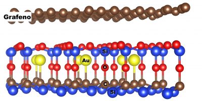
[Paper: Graphene on the oxidized SiC surface and the impact of the metal intercalation. J.E.Padilha, R.B.Pontes, F. Crasto de Lima, R. Kagimura, R. H. Miwa. Carbon, Volume 145, April 2019, Pages 603-613.]
Controlling the electronic properties of graphene on silicon carbide
A Brazilian scientific team performed a study based on supercomputer simulations that reveals a way to overcome the challenge of controlling the electronic properties of graphene. Solutions to this challenge can make a difference in the development of two-dimensional electronic devices – a dimension in which graphene, the one-atom thick network of carbon atoms, stands out for its properties.
In fact, graphene is an extremely tough, lightweight, flexible and transparent material. It is also an excellent conductor of heat and electricity. However, it is still difficult to control the concentration and flow of electric charges in graphene, which limits its use in electronics.
Solutions have been proposed to overcome this technological limitation of graphene. Some of them are based on the insertion of small amounts of metallic atoms that modulate the electronic properties of the material without impairing the other characteristics. The method is similar to the doping of silicon, practiced routinely in the manufacture of semiconductors for the electronics industry.

In the study that was recently reported in the scientific journal Carbon (impact factor 7,466), the Brazilian team investigated the structure and electronic properties of a graphene sheet on a silicon carbide (SiC) substrate – material often used to deposit or grow graphene. In this system, graphene remains attached to the substrate without chemical bonds, by means of distance-dependent weak attraction forces, called Van der Waals forces.
Given that in the production of graphene the presence of oxygen usually oxidizes the surface of the silicon carbide, the Brazilian scientists included in the simulations a layer of silicon oxide between the graphene and the substrate. Finally, in order to understand in detail the effect of the insertion of metallic atoms into this type of materials, the scientists added to the simulated system a layer of gold or aluminum atoms embedded in the oxide layer (in this case, Si2O5) in the interface region with graphene.
The researchers verified that the presence of the metallic layer modulates the concentration of the positive (so-called holes) and negative (the electrons) charge carriers in both the graphene sheet and Si2O5. In addition, the gold and aluminum atoms embedded in the Si2O5, which is semiconductor, induce the formation of conducting regions on the surface of this layer, in which the excess of electrons or holes is concentrated, induced by the presence of gold or aluminum, respectively. As a result, conductive channels are formed on the surface of the Si2O5, through which the charges flow.
![This two-dimensional map series shows the concentrations of electrons and holes in the graphene sheet in the two graphene systems on the silicon carbide surface finished in Si [(a) and (c)] and terminated in C [(b) and ( d)]; in the presence of an aluminum monolayer [(a) and (b)] and the other containing a gold layer [(c) and (d)].](https://www.sbpmat.org.br/site/wp-content/uploads/2019/06/dopagem-grafeno.jpg)
Based on these evidences, which were obtained mainly through computational simulations based on the Density Functional Theory, the paper suggests a way to control the concentration and flow of electrical charges on graphene sheets on silicon carbide substrates. The study also shows that the system studied (graphene sheet on oxidized silicon carbide with intercalated metal layer) can be a good platform for engineering electronic properties.
“The main contribution of the study is to show an efficient way of controlling the electronic properties of graphene on a solid surface covered with a metallic layer, by applying an external electric field,” says Professor Roberto Hiroki Miwa (Federal University of Uberlândia, UFU ), corresponding author of the paper. “We show that in addition to controlling the doping level of graphene, which is fundamental for the development of electronic devices in two-dimensional (2D) systems, the presence of the metallic monolayer allows the formation of conducting channels on the surface of the silicon carbide,” he adds. According to Miwa, the study may contribute to the development of faster, more accurate sensors, transistors and other electronic devices for charge transport and signal delivery.
At the beginning the work was motivated by the interest of UFU professors Roberto Hiroki Miwa and Ricardo Kagimura in understanding the graphene/oxide interfaces at the atomic level. The focus of the study matured as the authors delved into the scientific literature. As the volume and complexity of calculations increased, the researchers included new collaborators: a physics doctoral student at UFU (Felipe David Crasto de Lima) and professors from other institutions (José Eduardo Padilha de Sousa, from the Federal University of Paraná – Jandaia do Sul campus, and Renato Borges Pontes, Federal University of Goiás).

In order to perform the calculations that support the simulations, the authors used computational resources from the Brazilian National Center for High Performance Processing (CENAPD) and the SDumont supercomputer of the Brazilian National Laboratory of Scientific Computation (LNCC). The work was funded by federal agencies CNPq and CAPES and the state agency FAPEMIG (Minas Gerais).
