Interviews with plenary speakers of the XIV SBPMat Meeting: Nader Engheta.

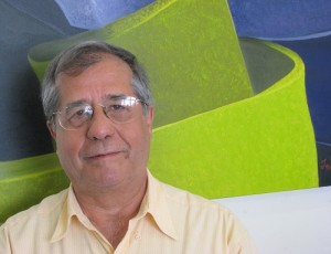
Photo of Prof. Nader Engheta superimposed with some of the images related to his research. Credit: University of Pennsylvania photographer Felice Macera.

Materials created by applying the state-of-the-art in materials science and engineering and nanotechnology can make light and other electromagnetic waves behave in an extraordinary way, becoming very useful for applications in several fields.

To talk about this issue in the XIV SBPMat Meeting, Professor Nader Engheta (University of Pennsylvania, USA) will be in Rio de Janeiro in the end of September. Engheta is a recognized world leader in research on metamaterials – man-made materials created through micro or nanoengineering, and capable of interacting with electromagnetic waves in ways not found in nature.  Metamaterials can sculpt the waves in order to achieve unconventional light-matter interaction.

In Rio de Janeiro, Engheta will talk about extreme scenarios generated from metamaterials: light traveling at full speed through artificial structures, one-atom-thick optical devices, metamaterials that perform mathematical operations, miniaturized circuits – optical rather than electronic – composed by metamaterials, and structures with effective refractive index near zero.

In his childhood in Tehran (capital of Iran), Nader Engheta developed a special curiosity to understand phenomena related to waves. This curiosity propelled him to attend and get a BS degree in Electrical Engineering at the University of Tehran. In 1978, he came to the United States to pursue his post-graduate (master’s and PhD degrees), also in Electric Engineering, carried in the prestigious Caltech (California Institute of Technology), in the United States. In 1982, he got his PhD diploma from Caltech, with a dissertation in the field of electromagnetism. After a post-doctorate at the same institution, Engheta worked as a scientist in the industry for four years, working again with electromagnetism.  Then he joined the faculty of the University of Pennsylvania in Philadelphia in 1987, and was swiftly promoted through the professorial ranks, and now he is the H. Nedwill Ramsey Professor of Electrical and Systems Engineering, with affiliations in the departments of Electrical and Systems Engineering, Physics and Astronomy, Bioengineering and Materials Science and Engineering.

Owner of an H number of 69 according to Google Scholar, Engheta has more than 21400 citations. Besides being author of 28 book chapters and numerous journal articles and conference presentations, Engheta is coeditor of the book “Metamaterials: Engineering and Physics Explorations”, released in 2006 by Wiley-IEEE publisher. In 2012, he chaired the Gordon Research Conference on Plasmonics.

His contributions to science and engineering have received important recognitions and distinctions from several entities, as the international society of optics and photonics, SPIE (“2015 SPIE Gold Medal”), the international union of radio science, URSI (“2014 Balthasar van der Pol Gold Medal”) and the international professional association of electric and electronic engineers, IEEE (“2015 IEEE Antennas and Propagation Society Distinguished Achievement Award”, “2013 Benjamin Franklin Key Award”, “2012 IEEE Electromagnetics Award”, “IEEE Third Millennium Medal”), among many other entities. He is also Fellow of six international scientific and technical organizations, namely, Materials Research Society (MRS), American Physical Society (APS), Optical Society of America (OSA), American Association for the Advancement of Science (AAAS), SPIE, and IEEE.  Engheta also received several teaching awards.  In 2006 the Scientific American Magazine selected him as one of the 50 Leaders in Science and Technology for his development of metamaterial-inspired optical nanocircuitry.

Here follows an interview with Professor Nader Engheta.

SBPMat newsletter: – In your opinion, what are your most significant contributions on issues related to the topic of your plenary lecture? Explain them very briefly and if possible, share references of resulting papers or books, or comment if these studies have produced patents, products, spin-off companies etc.

Nader Engheta: – I am very interested in light-matter interaction, and in my group we explore different methods in manipulating and tailoring interaction of waves with material structures, both in the optical as well as microwave domains.  I am very excited about all the research topics my group and I have been working on.  Some of these topics include (1) The optical metatronic nanocircuitry, in which we brought the notion of “lumped” circuit elements from electronics into the field of nanophotonics, developing a new paradigm in which material nanostructures may function as optical circuit elements.  In other words, “materials become circuits” working with optical signals.  In this way, nanophotonics can be modularized, in an analogous way as in electronics.  This allows one to perform optical signal processing at the nanoscale, (2) Metamaterials that can do math:  following our work on optical metatronics, we are exploring how properly designed materials (e.g., layered materials) can interact with light in such a way that one can do mathematical operations with light.  In other words, we are exploring the following questions:  Can materials be specially designed to perform analog processing with light at the nanoscale?  As light propagates through such properly designed material structures, would the profiles of the output signals resemble the results of certain mathematical operations (such as differentiation or integration) on the profiles on the input signals?  In other words, can we design materials for specific mathematical operations in order to do “photonic calculus” at the nanoscale?  (3) The extreme scenarios in light-matter interaction: this may include extreme dimensionality, like graphene photonics as the one-atom-thick platform for light manipulation, extreme metamaterials in which material parameters such as relative permittivity and relative permeability attain near-zero values.  This category of materials, which we have named epsilon-near-zero (ENZ), mu-near-zero (MNZ) and epsilon-and-mu-near-zero (EMNZ) materials, exhibit very interesting features in their response to electromagnetic wave interaction.

References:

  • N. Engheta, “Circuits with Light at Nanoscales:  Optical Nanocircuits Inspired by Metamaterials”, Science, 317, 1698-1702 (2007).
  • N. Engheta, A. Salandrino, A. Alu, “Circuit Elements at Optical Frequencies:  Nano-Inductor, Nano-Capacitor, and Nano-Resistor,” Physical Review Letters, 95, 095504 (2005).
  • N. Engheta, “Taming Light at the Nanoscale,”  Physics World , 23(9), 31-34 (2010).
  • A. Vakil and N. Engheta, “Transformation Optics Using Graphene,” Science, 332, 1291-1294 (2011).
  • A.Silva, F. Monticone, G. Castaldi, V. Galdi, A. Alu, and N. Engheta, “”Performing Mathematical Operations with Metamaterials,” Science, 343, 160-163 (2014).
  • M. G. Silveirinha and N. Engheta, “Tunneling of Electromagnetic Energy through Sub-Wavelength Channels and Bends Using Epsilon-Near-Zero (ENZ) Materials,” Physical Review Letters, 97, 157403 (2006).
  • N. Engheta, “Pursuing Near-Zero Response”, Science, 340, 286-287 (2013).
  • A.M. Mahmoud and N. Engheta, “Wave-Matter Interaction in Epsilon-and-Mu-Near-Zero Structures”, Nature Communications, 5:5638, December 5, 2014.

SBPMat newsletter: – Help us visualize the metamaterials developed by your group. Please choose one of your favorite photonic materials and tell us, very briefly, its composition, its main properties and its possible applications.

Nader Engheta: – One of the structures developed by my group is the optical metatronic nanocircuits for mid-IR regime (from 8 to 14 microns), in which we properly tailored and constructed nanorods of Si3N4 with specific widths and thicknesses, separated by a specific gap.  These arrays of Si3N4 nanorods function as collections of optical nanoinductors, optical nanocapacitors and optical nanoresistors in mid IR.  We demonstrated that such structures behave as nanoscale optical circuits, with functionality analogous to electronic filters, but here these material structures operate in the mid IR regimes.  We have shown how these structure operate as optical filters in the mid IR, offering exciting applications for future integrated optical devices and components.

Reference:

  • Y. Sun, B. Edwards, A. Alu, and N. Engheta, “Experimental Realization of Optical Lumped Nanocircuit Elements at Infrared Wavelengths,” Nature Materials, 11, 208-212 (2012)

Later, in collaboration with my colleague Professor Cherie Kagan and her group at UPenn, we extended this work into the near IR regime (from 1 to 3 microns).  In this case, we used the indium tin oxide (ITO) as the material of choice, with proper design and patterning of ITO nanorods. We also demonstrated that such ITO-based optical metatronic circuits function as an interesting platform for optical circuitry and filtering.  This can have exciting possibilities in the silicon photonics.

Reference:

  • H. Caglayan, S.-H. Hong, B. Edwards, C. Kagan, and N. Engheta, “Near-IR Metatronic Nanocircuits by Design,” Physical Review Letters, 111, 073904 (2013).

SBPMat newsletter: – If you want, leave a message or invitation to your plenary lecture to the readers that will attend the XIV SBPMat Meeting.

Nader Engheta: – One of the exciting features of doing science is the joy of search for unknowns and the thrill of discovery.  I always believe that we should follow our curiosity and our passion for discovery. Also, in science and technology it is important to maintain the balance between the complexity and the simplicity in search for solutions to scientific inquiry.

More
Plenary lectures: world-class science with social impact.

Plenary lectures: very good attendance.

The scene repeated itself daily while the event lasted: around 8.30 a.m. and 2 p.m., under the strong João Pessoa sun, lines of hundreds of participants entered the convention center and settled at the refrigerated plenary room. There, scientists with outstanding careers, attested by their H indexes of values ranging from 40 and 73, coming from England, France, Germany, Italy, Portugal and United States, shared their knowledge about matters on which they are, without a shadow of a doubt, qualified specialists.

In the event’s final plenary lecture, Robert Chang, professor at the first department of materials science in the world, at Northwestern University, resumed two subjects that had been explained by Professor Arana Varela in the memorial lecture, and which permeated almost every plenary. The first one is the essential role that materials field and, in particular, nanotechnology play in meeting, in a sustainable way, the needs and demands of humanity in healthcare, food, transportation, security and communication. The second subject is the need for collaboration to face this challenge of the 21st century.

In this context Chang, who was president of the American Materials Research Society (MRS) and founded in 1991 the International Union of Materials Research Societies (IUMRS), called upon the young Brazilians [see video below] to be part of a global network released in 2012, which promotes the interaction of young researchers in the field around these global challenges through a biennial conference and virtual platforms.

However, Chang said, the scientific collaboration among physicists, chemists, engineers, mathematicians, biologists and other researchers to develop the necessary technologies is insufficient. It is also necessary, he added, to rely on the collective, global effort from governments, companies, communities, families and individuals to deploy these technologies on peoples’ daily lives. “That requires education”, he said. For the last 20 years, the scientist has conducted the Materials World Modules Programme, which developed interactive educational material about Materials and Nanotechnology for middle and high-school students.

Nanomedicine

Luís Carlos

Portuguese professor Luís Carlos, from the University of Aveiro, brought to XIII SBPMat Meeting many examples about the applications of nanotechnology in the healthcare field that are making a difference, or may make a difference in the short-term.

Being an expert in luminescent materials, which emit light not derived from heat, the scientist showed in his plenary lecture that these materials are already of great use in medical diagnosis. Luminescent organic complexes, for example, are marketed as contrast agents for magnetic resonance imaging, and as markers for fluoroimmunoassays (used in pre- and neonatal screening and detection of proteins, viruses, antibodies, drug residues etc.).

Besides, Luís Carlos said, luminescent nanoparticles (quantum dots and nanocrystals with lanthanide ions) emerge in diagnostic techniques and also in treatments, such as the hyperthermia process. This consists in the exposition of biological tissues, usually cancerous cells, at temperatures above 45°C, causing their deaths, with minimum collateral lesions to surrounding normal tissues. With proper temperature monitoring and control, the technique can soon become popular.

For the last few years, there have been efforts to develop nanothermometers that measure intracellular temperature to service this and other applications, not only regarding Nanomedicine, but also in fields such as Microelectronics, Photonics and Microfluidics. A successful example, presented by Luís Carlos at the plenary, is the development of a nanometric platform composed by nanorods, which work as thermometers, with gold nanoparticles on its surface, which function as heaters. This is a platform that, in contrast to its small size, can bring great benefits to the improvement of the technique of hyperthermia and the study of the processes of heat transfer at the nanoscale.

LEDs and other gallium nitride devices: savings of 25% in the global electricity consumption

Sir Colin Humphreys

When the Nobel Prize in Physics was announced for three Japanese scientists whose works were essential for the development of LED white light bulbs, those who had participated in XIII SBPMat Meeting certainly remembered the plenary lecture by Sir Colin Humphreys from University of Cambridge. The material chosen by the laureates when they decided to face the challenge of creating the blue LED that would allow the white light emitting LED was gallium nitride, which was also the object of Sir Colin’s lecture.

Professor Humphreys is an expert in this material. He created and directs a research center in Cambridge devoted to gallium nitride, and he also founded two spinoff companies to commercially exploit the technology developed by his research group and manufacture LEDs grown on relatively large silicon wafers, of about 15 cm, for low cost lighting. In 2012, the spinoffs were purchased by Plessey, a manufacturer of products based on semiconductor materials with over 50 years in the market. Now these LEDs are produced by Plessey in the United Kingdom.

The gallium nitride LED bulb currently offers one of the longest shelf lives in the market – 100,000 hours of use, equivalent to 69 years without switching the bulb, against 1,000 hours of life of the incandescent light bulb and 10,000 of the fluorescent. These LEDs also provide high energetic efficiency, ranging from 100 to 200 lumens (amount of light emitted in a second) per watt of power consumed.

At the plenary lecture, Sir Colin showed that the widespread use of LEDs in lighting would result in savings of about 15% in the total electricity consumed on the planet, and thus in a substantial decrease in emissions of carbon dioxide. In fact, lighting is one of the few segments where devices with high-energy efficiency are not yet universal.

More energy can be saved, Professor Humphreys said, by replacing silicon by gallium nitride in various electronic devices. In total, Humphreys concluded, up to 25% of all electricity used in the world today could be saved, reason why, added to the other applications of gallium nitride in the healthcare field, it was enough for the British scientist to state that this manmade material is one of the most important in the world.

Organic semiconductors: OLEDs and solar cells in the spotlight

Karl Leo

Just like it happens with LEDs, the OLEDs, which are manufactured with organic materials justifying the “O” in the acronym, directly convert electricity into light and are, therefore, devices with high potential efficiency, which has been improved every year. Having each one particular advantages, LEDs and OLEDs already compete in certain markets, such as the one of displays and, in a more incipient manner in the case of organics, in the lighting market.

Along with organic solar cells, OLEDs were the focus of Karl Leo’s plenary lecture. He is a professor at the German TU Dresden and at the Saudi Arabian KAUST universities, and wrote over 550 papers with 23,000 references and 50 patent families. He is also founder of 8 spinoff companies, such as Heliatek and Novaled, which manufacture organic solar cells and OLEDs, respectively.

Professor Leo showed an important quantity of results achieved by his research groups, regarding the improvement of organic semiconductor devices. Along with his collaborators, Karl Leo has developed an extensive work about doping organic semiconductors in the transport layers of OLEDs and solar cells to increase significantly their electrical conductivity. This work resulted, for example, in obtaining white light-emitting OLEDs with energetic efficiency greater than those of fluorescent tubes.

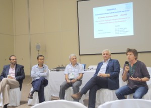
From the left, A. Salleo, F. So, R. Faria, H. von Seggern and J. Nelson.

Karl Leo was not the only internationally renowned scientist in João Pessoa in the field of organic semiconductors. On Wednesday afternoon, a roundtable organized by Symposium D gathered four of these specialists: Alberto Salleo (Stanford University), Franky So (University of Florida), Heinz von Seggern (TU Darmstadt) and Jenny Nelson (Imperial College London). Moderated by a prominent Brazilian scientist of the field, Roberto Mendonça Faria, professor at the São Carlos Institute of Physics at University of São Paulo and SBPMat president, the session gathered dozens of participants of the meeting, of various ages, that actively participated at the debate.

The discussion was around the challenges of organic electronics, from basic research to mass production (or individual production, as pointed out by a young man of the public drawing attention to the 3D printing techniques). Various subjects of the scientific, industrial and social fields were addressed bythe panelists based on the audience’s questions. “Fortunately, there are challenges for Materials Science. Unfortunately, there are challenges for mass production,” Professor Faria summed up, resuming, somehow, one of the first lines of the round table, in which Professor Jenny Nelson lamented that the scientific community celebrated a lot more the development of a device that works than the understanding of why a particular device did not work.

Alberto Salleo

Alberto Salleo, creator of a group in Stanford that studies the relation between structure and properties on polymeric semiconductors to better understand the charge generation and transport, also delivered a plenary lecture at the event. In the lecture, Salleo cast doubt on the universality of a widespread assumption that links a high degree of crystallinity (or order) in the microstructure of these polymers to a higher charge mobility, or better performance of the devices. The scientist showed that the disorder is good for organic solar cells and cited examples of almost amorphous semiconducting polymers having similar performance to others much ordered.

Professor Salleo presented a model developed by his group to show how the charge transport in organic semiconductors works, since they are materials with heterogeneous microstructures, where disordered and ordered aggregates coexist with each other and with long polymer chains. In order to have high charge mobility, Salleo revealed, the important thing is for the aggregates to connect among themselves, which happens through the polymeric “spaghetti”.

Order, but without periodicity

Jean-Marie Dubois

The quasicrystals are far from the disorder, but also outside the traditional crystalline order. These materials were the general theme of the plenary of French researcher Jean-Marie Dubois, from Institut Jean Lamour, whose experience in this field was recognized by the scientific community through the creation of the “Jean-Marie Dubois International Award”, given every three years to research works related to quasicrystals.

First, Dubois presented an introduction to quasicrystals, materials in which the atoms are grouped into unit cells in patterns which are ordered (which may be determined by algorithms) but not periodic (never repeat themselves). Beautiful scientific and artistic images intermixed in Dubois’ presentation allowed the audience to view this aperiodic order.

The lecturer also paid homage to Dan Shechtman, who discovered quasicrystals in 1982 and, after many fights and resistance in the scientific community, eventually won the Nobel Prize in Chemistry in 2011 and generated a big shift in the vision of ordered condensed matter. Today, quasicrystalline materials are synthesized and used in various products, such as auto parts and pans, to improve their thermal conductivity, adhesion, friction, corrosion resistance etc. It is noteworthy that Dubois is among the pioneers in filing patents targeting applications of quasicrystals.

The quasicrystalline order can be observed in various types of materials. In the lecture at the XIII SBPMat Meeting, Dubois addressed, in particular, metal alloys formed by three elements (A, B and C), in which A – B and B – C form chemical bonds, while B and C repel themselves. Named by Dubois “push-pull alloys”, these materials can form very complex intermetallic compounds, with up to hundreds of atoms per unit cell. Among these, only a few can further increase their complexity to form a quasicrystalline order, which results in unique properties and open up possibilities for new applications.

Computer simulation

Roberto Dovesi

In another plenary lecture of the XIII SBPMat Meeting, supporters of computer simulation as a complement to the experimental work in the investigation of material properties, and those interested in using it, were able to hear from Professor Roberto Dovesi (Università di Torino) that this dual approach is worthwhile.

Dovesi is one of the creators of CRYSTAL, a computational tool that allows the characterization of crystalline solids from the point of view of quantum mechanics, through ab initio calculations. The first version of the program was developed from 1976 onwards and released in 1988, making CRYSTAL the first periodic code distributed publicly to the scientific community. Now in its seventh version, the program allows the study of elastic, piezoelectric, photoelastic and dielectric properties, polarizability and hyperpolarizability tensors, IR and RAMAN spectrum, structure of electronic and phononic bands, among other properties.

The Italian chemist highlighted the affordable price and high working speed of today’s computers that are suitable to run such programs. As an example, he cited a machien recently acquired by his research group for computer simulation, which, costing around 6,500 euros, is able to do long calculations in a few hours with its 64 cores. Supercomputers are not necessary, Dovesi said, and are less robust. As for software, Dovesi remarked that today the field of materials has powerful, robust, easy-to-use programs at affordable prices (a basic license of the latest version of CRYSTAL, for example, costs 600 euros.

Minientrevistas com palestrantes do XII Encontro da SBPMat: Elson Longo da Silva (Unesp).

O professor Elson Longo. Crédito: divulgação.

Elson Longo é professor da pós-graduação na Universidade Estadual Paulista Júlio de Mesquita Filho (Unesp) e Professor Emérito da Universidade Federal de São Carlos (UFSCar). Coordena o Centro Multidisciplinar para o Desenvolvimento de Materiais Cerâmicos (CMDMC) e o Instituto Nacional de Ciência e Tecnologia dos Materiais em Nanotecnologia (INCTMN).

Químico formado pela Unesp em 1969, com mestrado e doutorado em Físico-Química pela Universidade de São Paulo (USP), Longo conta com mais de 780 artigos publicados em revistas internacionais, que totalizam mais de 11.180 citações. O professor já foi orientador de mais de 50 mestres e mais de 60 doutores enquanto professor da UFSCar (1989-2005) e da Unesp (a partir de 2005).

Da sua carreira como pesquisador da área de Materiais, Longo destaca uma série de contribuições realizadas nos últimos vinte anos: varistores a base de óxido de zinco, óxido de estanho e titanato de cálcio e cobre; sensores; materiais fotoluminescentes a base de titanatos e tungstato; filmes finos ferroelétricos para utilização em memórias, e materiais fotodegradadores (materiais semicondutores). Também na área de Materiais, Longo participou, junto a empresas da indústria de refratários e siderúrgica, do desenvolvimento de novos tipos de refratários, pisos e azulejos e de cerâmica artística.

É membro titular da Academia Brasileira de Ciências, empossado neste ano, membro da Academia de Ciências do Estado de São Paulo e membro da Academia Internacional de Cerâmica (World Academy of Ceramics).

Atualmente é membro do Conselho da SBPMat. Foi presidente da sociedade de 2004 a 2005.

No XII Encontro da SBPMat, Longo será honrado com a Palestra Memorial “Joaquim Costa Ribeiro”, na qual falará sobre a evolução da pesquisa em Materiais no Brasil.

Segue uma breve entrevista com o palestrante.

Boletim da SBPMat (B.SBPMat): – O senhor tem vasta experiência em projetos realizados junto a empresas. O que teria a comentar sobre a relação da área de Materiais e a indústria no Brasil nesses 40 anos de Engenharia de Materiais? A inserção de engenheiros de Materiais na indústria tem ajudado a melhorar a qualidade, variedade e valor agregado dos produtos brasileiros?

Elson Longo(E.L.): – A área de Materiais evoluiu sobremaneira após a fundação e consolidação da primeira turma de Engenharia de Materiais da UFSCar. Este curso criou no país novas perspectivas para a indústria de um modo geral, pois contemplava três áreas extremamente carentes de especialistas: cerâmica, polímeros e compósitos. Na área de metais já existiam os engenheiros especializados formados em diferentes universidades do país. Vamos tomar somente dois exemplos: a indústria de refratários prosperou e tornou-se competitiva internacionalmente, o mesmo ocorrendo para a indústria de polímeros. Os produtos brasileiros são competitivos no mercado nacional e internacional em função do trabalho dos engenheiros de Materiais e demais categorias de engenharia que trabalham em consonância.

B.SBPMat: – Na sua visão, quais os principais resultados da evolução da formação de recursos humanos na área de Materiais nesses 40 anos no Brasil?

E.L.: – Mais importante que a formação de recursos humanos foi a estruturação de cursos de Engenharia de Materiais em nível de graduação e pós-graduação. Estes cursos hoje estão homogeneamente distribuídos pelo país beneficiando sobremaneira a nossa indústria.

B.SBPMat: – Como você consegue manter uma produtividade científica tão alta e com tantas citações?

E.L.: – A nossa produtividade é fruto de um trabalho em equipe que envolve pesquisadores de São Paulo, Rio Grande do Sul, Paraná, Rio de Janeiro, Minas Gerais, Goiás, Brasília, Sergipe, Paraíba, Rio Grande do Norte, Piauí, Maranhão e Pará. Devo destacar também as interações internacionais que proporcionam grandes oportunidades ao grupo de mostrar o nosso trabalho para a comunidade internacional.

B.SBPMat: – Enquanto participante ativo da história da SBPMat, o que você destacaria dos onze anos de existência da sociedade?

E.L.: – O principal ponto da SBPMat é a harmonia que existe entre os pesquisadores de todos os níveis e a saudável troca de informação entre os mesmos. Por outro lado, a SBPMat desde sua origem tem uma forte participação dos pesquisadores do exterior, o que a coloca na vanguarda do conhecimento.

Informações sobre a palestra de Elson Longo no XII Encontro da SBPMat
Título: “Evolução da pesquisa em Materiais no Brasil”
Resumo: Desde a fundação do curso de Ciência dos Materiais na UFSCar, São Carlos (SP), o país vem evoluindo de modo constante nesta área de conhecimento. É importante ressaltar que esse curso catalisou pesquisadores de Engenharia, Química e Física para o desenvolvimento de materiais cerâmicos, poliméricos e compósitos. Por outro lado, houve também uma ampliação dos cursos de Materiais a nível de graduação e pós graduação, o que contribuiu enormemente para o desenvolvimento da área. Com essa nova estrutura, houve a necessidade da criação da Sociedade Brasileira de Materiais, que vem evoluindo de modo positivo ao longo dos últimos 10 anos.
Quando: 29 de setembro (domingo) das 20h00 às 21h00, após a abertura do evento e antes do coquetel.