Some of the challenges of the next generation of smartphones, sensors and other electronic devices can be solved with the help of nanomembrane microtubes (sheets made from various materials with nanometric thicknesses and micrometric lateral dimensions, which can be self-rolled and form microtubes).
In the city of Campinas (São Paulo State), at the Brazilian Nanotechnology National Laboratory of the National Center for Research in Energy and Materials (LNNano / CNPEM), a group of scientists has developed expertise in processes for the synthesis, manufacture and characterization of nanomembranes and their applications. In papers published in January and February of this year in the journals Nano Letters and Nature Communications, the authors explore some nanomembrane potentials, mainly related to their flexibility and dimensions, to develop new memristors and transistors – two widely used electronic devices.
More precisely, the LNNano researchers show that nanomembrane microtubes can be key parts in the manufacture of promising components using organic and hybrid materials (organic-inorganic) such as memristors and transistors. Thus, the novelties proposed in the articles can contribute to the development of even smaller, flexible, portable, cheaper devices and equipment that combine better performance and more low energy consumption features.
In an interview with the B-MRS Newsletter, Carlos Cesar Bof Bufon, corresponding author of both articles, talks about the scientific, technological and social impact of the research and about the skills and infrastructure involved in carrying it out. Bufon is a researcher and head of the Devices Division at LNNano/CNPEM.
B-MRS Newsletter: The articles present advances, developed at LNNano, in technologies for electronic devices (transistors and memristors). In your opinion, what are the main technological and/or scientific contributions of these articles?
Carlos Cesar Bof Bufon: The work entitled “Ambipolar Resistive Switching in an Ultrathin Surface-Supported Metal–Organic Framework Vertical Heterojunction” published in Nano Letters (DOI: 10.1021/acs.nanolett.9b04355), reports the development of a new type of memristor using structures called Surface-Supported Metal-Organic Frameworks (SURMOFs). SURMOFs are hybrid structures composed of metallic ions connected by organic ligands. The structure is highly organized on surfaces covered with chemically active self-assembled monolayers (SAMs). There are more than 70 thousand types of metal-organic structures (MOFs) that can be prepared as SURMOFs to confer new features to electronic devices. In addition to the unique properties, its considerable mechanical flexibility and low cost arouse interest in the scientific community for applications. However, in the case of a hybrid material consisting of organic and inorganic elements, the integration of this class of nanomaterials becomes a technological challenge. To circumvent this limitation, this work presents a new architecture for the integration of these SURMOFs structures for the development of a new type of memristor. The proposed architecture is based on the upper electrical contact of SURMOF HKUST-1 ultrathin films using self-rolled metal nanomembranes (microtubes). The SURMOF films explored in this work have thicknesses of the order of 20 nanometers. This new architecture opens up promising paths in the area of electronic devices based on SURMOFs, as well as providing a technological platform for conducting studies not yet reported in the literature for this class of materials. For example, the investigation of how electrical charges are conducted in layers of ultrathin SURMOFs.

The work entitled “Edge-driven nanomembrane-based vertical organic transistors showing a multi-sensing capability” published in Nature Communications (doi: 10.1038/s41467-020-14661-x) presents the development of a vertical organic transistor platform. Transistors are the main components for electronic circuits and processors. Compared to inorganic transistors, the organic ones have the advantages of low-cost and easy fabrication, which makes them attractive for flexible electronic devices in several areas. A significant advantage of vertical transistors is their easy integration with light-emitting devices and photodetectors in the formation of integrated optoelectronic systems. The devices presented in this work were processed entirely using conventional microfabrication and photolithography techniques, which is an advantage of technological feasibility. One of the main differences of these new transistors is related to the use of self-rolled metallic nanomembranes as drain electrodes, thus promoting the formation of a smooth mechanical contact with the organic semiconductor layer. In this architecture, the organic semiconductor layer can reach thicknesses below 50 nanometers. The manufactured devices showed high current densities (~ 0.5 A / cm2) with low operating voltages (≤ 3 V). Based on our theoretical study, it was possible to predict an improvement in the structure of the transistor, resulting in projections of devices with current densities of up to 10 A / cm2. Such values, obtained at low operating voltages on a platform composed of active organic layers, highlights the potential of these devices to be integrated with flexible and portable electronic applications in the future. Besides, the new transistors were able to detect different levels of humidity and light, thanks to the device platform based on self-rolled nanomembranes. Therefore, the developed transistors also have great potential for advancing next-generation sensor technology.
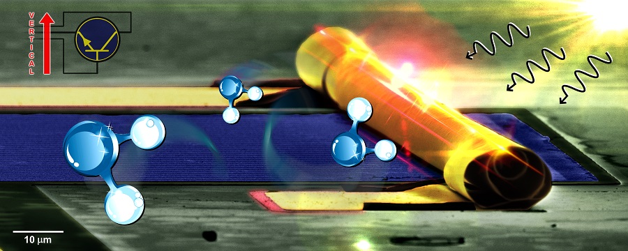
Scanning electron microscopy image (artificially colored) of the vertical organic transistor based on rolled nanomembrane (yellow tones). The incident radiation and the water molecules (artificially placed) illustrate the multiple sensitivity characteristics of the new electronic device.
B-MRS Newsletter: How could the results of the articles impact people’s daily lives (social impact)? Do you think that the proposed technologies could replace those currently used or create new applications? If so, what would be the advantages of these new technologies developed at LNNano? Would it still need many steps to bring the results of the articles to the market?
Carlos Cesar Bof Bufon: Memristor is considered one of the four fundamental electronic components. On a computer, it is capable of performing information processing and storage functions. In this work, the behavior of a memristor was observed in conditions of high relative humidity (between 90-70%). Analogous to a sponge, the water molecules present in the environment are absorbed by SURMOF nanopores. In a given electric field, these molecules facilitate the conduction of electrons within the material by changing its electrical resistance. The difference in electrical resistance can reach 1 million times using low operating voltages, less than 2 V. In a practical application, this difference can correspond to the binary states 0 and 1. The total fabrication of the device was carried out with conventional techniques photolithography, compatible with industrial scale production. The fact that it depends on the humidity for its operation does not limit its commercial application, as this can be easily bypassed through encapsulation processes, common in the electronic device industry.
The manufacture of organic transistors in vertical architecture using curled nanomembranes as drain electrodes allows the reduction of the region of interest to less than 50 nanometers (more than a thousand times less than the thickness of a hair). This implies a significant advance in the electronics industry, because the portability of electronic applications, such as smartphones, computers and televisions, depends on the reduction in the number and size of transistors. The mechanism of operation of the device reported in this work expands the current understanding of vertical organic transistors, showing that current densities can be improved by performing careful manipulations in the spatial structure of the intermediate metallic electrode (source). Besides, the preparation of transistor microchips was carried out using microfabrication techniques compatible with the industrial scale. Thus, these devices can be easily integrated into electronic applications with a few additional steps, such as encapsulating microchips, to prevent degradation of organic materials.
The two concepts of devices based on nanomembranes expand the possibilities for the use of hybrid materials in electronics. As much as there is a tendency to substitute one technology for another, the concepts developed in our works seek to open new frontiers and possibilities through the design of functional structures from their fundamental elements such as atoms and molecules.
All the technologies that we develop in the area of devices at LNNano/CNPEM are firmly grounded in two focus: the understanding of the fundamental concepts that govern the properties of the components, and their technological application. These two papers started fundamentally from scratch. In terms of technology readiness level (TRL), the devices have reached the functional validation of the components in the laboratory environment. Within the TRL scale, we achieved the fourth level out of a total of 9 – the latter being commercialization. It is also worth mentioning that the next level of development must involve the participation of the productive sector, which is who can accelerate the research towards the market.
B-MRS Newsletter: Briefly tell us the story of the works reported in the two articles: how and when the idea came up, whether it was necessary to gather very different skills, the infrastructure used, curiosities etc.
Carlos Cesar Bof Bufon: The works are the result of different stories, but were developed in the same research group sharing the idea of exploring the potential of nanomembranes in the area of functional devices. This theme is part of my Young Researcher project financed in 2016 by FAPESP. The idea of applying SURMOFs as a memristor, using nanomembranes as the top contact, was developed together with the post-doctorate Dr. Luiz Gustavo Simão Albano. Our research group started evaluating the feasibility of using SURMOFs as functional materials in devices about 3 years ago. Since then, the group has been continuously establishing the implementation of synthesis and integration routes for applications in the areas of electronic components. The work was carried out entirely at LNNano/CNPEM, and has a list of co-authors who actively contributed to making this work possible: Tatiana P. Vello (growth of SURMOFs), Davi HS de Camargo (manufacture of devices and illustrations), Ricardo ML da Silva (device manufacturing), Dr. Antonio CM Padilha (DFT simulations) and Prof. Dr. Adalberto Fazzio (DFT simulations).
The work with the transistor follows the same pattern as the memristor – a combination of functional materials and nanomembranes. About 15 years ago, I became interested in the potential of using nanostructured layers as fundamental blocks in vertical electronics. Once I was aware of the work of Prof. Ivo Humlegem, from UFPR (died 2018), in the area of vertical transistors, a series of advantages and challenges caught my attention. The idea of the work came by anticipating that an improvement of the performance of vertical transistors could be achieved with the use of a drain electrode based on nanomembrane combined with a patterned intermediate electrode (source) using photolithography. In May 2018, Dr. Ali Nawaz (a former student of Prof. Ivo!), started the execution of the project at LNNano/CNPEM. Being a complex project, the advanced infrastructures for processing and characterizing LNNano/CNPEM devices were essential. And like the memristor, the research depended on a set of varied expertise. During the project, Dr. Leandro Merces provided critical assistance in the investigation of the theoretical aspects of the devices, while collaborators Davi Camargo (specialist in microfabrication) and Denise de Andrade (graduate trainee at the State University of Ponta Grossa), provided the entire work the necessary technical support.
[Papers: Ambipolar Resistive Switching in an Ultrathin Surface-Supported Metal–Organic Framework Vertical Heterojunction. Luiz G. S. Albano, Tatiana P. Vello, Davi H. S. de Camargo, Ricardo M. L. da Silva, Antonio C. M. Padilha, Adalberto Fazzio, Carlos C. B. Bufon. Nano Lett. 2020, 20, 2, 1080-1088. https://doi.org/10.1021/acs.nanolett.9b04355 and Edge-driven nanomembrane-based vertical organic transistors showing a multi-sensing capability. Ali Nawaz, Leandro Merces, Denise M. de Andrade, Davi H. S. de Camargo & Carlos C. Bof Bufon. Nature Communications volume 11, Article number: 841 (2020). https://www.nature.com/articles/s41467-020-14661-x ].