Graphene-based products are already being used by manufacturers, from heat-dissipating helmets to antistatic packaging. However, this wonderful material, as it is often called, still has much to deliver to society. As it is two-dimensional, flexible and excellent conductor of electricity, among other properties, graphene can be the basis of a series of high-performance miniaturized electronic and optoelectronic devices. However, this requires producing, at an industrial scale, a graphene whose network of atoms is free of unwanted impurities, but which contains, besides the carbon inherent in the graphene, small amounts of other elements (doping) in order to control its electronic properties.
In a work totally carried out in Brazil, a scientific team has proposed a process that can help produce large-scale graphene that is suitable for electronic devices. “The process developed in our group allows us to improve and adjust the graphene properties, as well as the removal of contaminants from its surface,” said Professor Claudio Radtke (UFRGS), corresponding author of an article reporting the study, recently published in The Journal of Physical Chemistry C.

The team acquired graphene samples produced by chemical vapor deposition (CVD) and transferred to silicon substrates. This technique is currently one of the most suitable for large-scale production of relatively large area graphene sheets, but it leaves residual impurities and generates defects in the graphene. To remove impurities, it is common to apply a heat treatment in an atmosphere of carbon dioxide (CO2), which is efficient in removing contaminants, but ends up generating new defects in the graphene sheet. The good news is that these defects can be neutralized (passivated).
While looking for strategies to passivate these defects, then PhD student Guilherme Koszeniewski Rolim found a scientific paper from 2011, which pointed to, through theoretical calculations, the possibility of using nitric oxide (NO) to passivate graphene defects with nitrogen atoms, while doping it to modulate its electronic properties (mainly transforming it into a semiconductor material, an essential condition for using graphene in electronic devices).
The team then decided to experimentally verify the theoretical prediction and, after performing the traditional treatment with CO2 at 500 °C, they applied a second heat treatment to the samples, this one in nitric oxide atmosphere and at different temperatures, from room temperature to 600 °C.
After the process, the researchers used various characterization techniques to check the results and gladly confirmed that nitrogen doping had taken place and that it had passivated the defects, thus improving the material’s electronic properties. However, the researchers also noted an unwanted effect of nitric oxide treatment: etching of graphene sheets at some points. After much scientific work, the team was able to determine the cause. During heating, there was a conversion of NO to NO2, which, as it is a much more reactive compound than the former, eventually oxidized the graphene.
However, the Brazilian team found a solution to this problem. The “eureka” moment occurred as the researchers were trying to determine the amount of nitrogen atoms that had been incorporated into graphene using a technique based on the analysis of nuclear reactions triggered by the effect of an ion beam on the graphene samples. In order to apply this technique, the team had to use an isotopically enriched nitric oxide in the heat treatment, which has a purity of 99.9999% instead of 99.9% of the gas previously used.

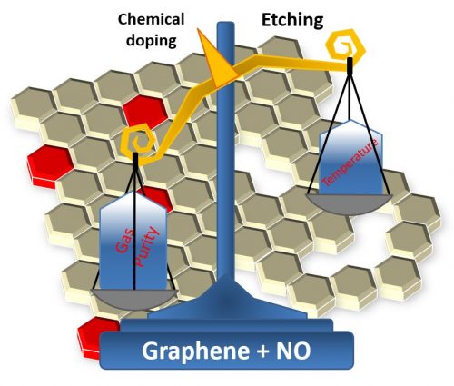
The analysis did not yield the expected results as it failed to quantify nitrogen, which was below the detection limit. However, the use of the enriched gas eventually brought great satisfaction to the team. Indeed, when the researchers compared the electronic properties of both sample types, they found that graphene treated with enriched gas always had superior properties. “Initially, such a result created much confusion in the interpretation of the results,” says Professor Radtke. “But after a few more experiments, it became one of the most important points of the article, highlighting the importance of gas purity during processing,” he adds. Specifically, the conclusion was that by properly controlling the temperature and purity of the gas during the treatment one can eliminate the problem of oxidative graphene degradation.
Thus, based on solid knowledge and scientific method, as well as some serendipity, the UFRGS team was able to develop a process of waste removal, defect neutralization and graphene doping, which improved the electronic properties of the material without producing deleterious side effects. Because it is a heat treatment in a gas atmosphere, a step that is now part of the industrial production of graphene, the process proposed by the Brazilian team could be easily applied in the production of graphene sheets for devices.
“The insertion of heteroatoms (such as nitrogen) into the graphene network without the degradation of its properties is especially important in the production of optoelectronic devices, high speed transistors, low power electronics and photovoltaic cells,” says Radtke, noting that manufacturing these graphene-based devices may be a reality in years to come. “The Graphene Flagship (European consortium of industries, universities and institutes) has announced the implementation of a pilot plant to integrate graphene at different production stages of devices as early as 2020,” comments the professor from UFRGS.
The study, which was funded by the Brazilian agencies CNPQ (mainly through INCTsNamitec and INES), Capes and Fapergs, was developed within the PhD in Microelectronics by Guilherme Koszeniewski Rolim, held at the UFRGS Graduate Program in Microelectronics and defended in 2018. The experimental work was carried out at the UFRGS Solid Surface and Interfaces Laboratory and the Brazilian National Synchrotron Light Laboratory.
[Paper: Chemical Doping and Etching of Graphene: Tuning the Effects of NO Annealing. G. K. Rolim, G. V. Soares, H. I. Boudinov, and C. Radtke. J. Phys. Chem. C, 2019, 123, 43, 26577-26582. https://doi.org/10.1021/acs.jpcc.9b02214.]

Ricardo Ruiz Martuci
Olá bom dia! Tudo bem? Venho pedir um help com os protocolos de dopagem com o grafeno!
Sou cirurgião-dentista com Mestrado e Doutorado pela USP/São Paulo e agora estou na Universidade do Porto em Portugal fazendo o meu pós-doutoramento na área de materiais e prótese por aqui. Pois bem, iremos trabalhar com um material cerâmico (dissilicato de lítio – o material mais usado e estudado para as cerâmicas odontológicas), uma material polimérico (PMMA) e um material híbrido, que seria a mistura dos dois. Teremos amostras sem dopagem com o grafeno e amostras dopadas com o grafeno por incorporação em 0,75wt%. Realizarei testes mecânicos de microdureza e rugosidade superficial, corrosão por névoa salina, MEV, testes bacteriológicos específicos, visto o potencial bactericida do grafeno entre outros testes laboratoriais envolvidos no ptojeto. O que acontece é o seguinte, a dúvida dos engenheiros por aqui é, qual o melhor protocolo de dopagem com o grafeno que podemos ter com os materiais cerâmicos, com os poliméricos e com os híbridos? Tem muita coisa em revisão de literatura e realmente ficamos meio “perdidos” com essa etapa significativa do protocolo de dopagem! Se puderem me responder ou dar uma orientação, agradeceria imensamente. Muito obrigado e parabéns pela publicação do trabalho!
Afonso
Sensacional. Poderiam fazer uma parceria com o MackGraphe para expandir o uso do grafeno em estudo.
Ricardo Ruiz Martuci
Como devo proceder para essa parceria com o MackGraphe?
Agradeço!
Ricardo