
|
|||||||||||||||||||||
|
|||||||||||||||||||||
|
|
|||||||||||||||||||||
|
|||||||||||||||||||||
|
[Paper: Nanocatalysts for hydrogen production from borohydride hydrolysis: graphene-derived thin films with Ag- and Ni-based nanoparticles. Leandro Hostert, Eduardo G. C. Neiva, Aldo J. G. Zarbin, Elisa S. Orth. J. Mater. Chem. A, 2018,6, 22226-22233. DOI 10.1039/C8TA05834B]
Graphene and nickel films, the best catalysts for hydrogen production
Thousands of vehicles powered by hydrogen gas already circulate in some regions of the world releasing only water through the exhaust pipes. As a fuel or source of energy, hydrogen is in fact an extremely clean (does not generate harmful emissions) and efficient option (it can produce more energy than any other fuel). However, pure hydrogen does not exist in nature on Earth. It needs to be produced, and most of the hydrogen-generating methods known to date have both economic and ecological drawbacks.
An alternative to these methods was recently presented by a team of researchers from the graduate program in Chemistry of the Brazilian Federal University of Paraná (UFPR). These scientists have proposed a clean, efficient, simple and inexpensive method to produce hydrogen. The team developed new catalysts (compounds that modify the speed of a chemical reaction without being consumed during the reaction), made of graphene and metal nanoparticles, which made hydrogen production feasible through the hydrolysis of borohydride – a chemical reaction still little used in hydrogen generation, notwithstanding its enormous potential as it is clean and very simple.
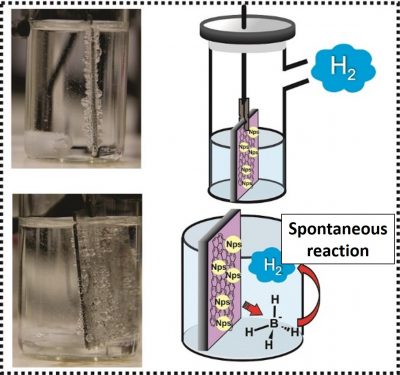
In this reaction, which is performed at room temperature, sodium borohydride (NaBH4) molecules, spontaneously react with water molecules generating hydrogen (H2) molecules. The process takes place in only one step, and is performed with catalyst materials, which accelerate the reaction rate.
“The main contribution of this work is the possibility of H2 generation through thin films of graphene nanocomposites,” says Professor Elisa Souza Orth, corresponding author of an article on the work, recently published in the Journal of Materials Chemistry A (impact factor = 9,931). “Nanocomposites of carbon-based materials and metallic nanoparticles have shown many promising applications and we have shown that for the less exploited borohydride hydrolysis they could also be used efficiently,” she adds.
Among the thin film catalysts produced by the UFPR team, the ones that presented better performance were those of reduced graphene oxide with nickel nanoparticles (rGO/Ni). In fact, this nanocomposite, produced with a relatively inexpensive metal, performed better than most of the catalysts previously reported in the scientific literature, including those prepared with noble metals, which cost much more.
In general, this means that small amounts of rGO/Ni (some tens of mg) generated large volumes of hydrogen (400 ml) in a short time (5 hours).
In addition, the films developed by the Brazilian team presented another important characteristic for a catalyst: they can be easily removed from the reaction vessel, washed and dried without damage, thus allowing their reuse. “In this work, we were able to reuse the same nanocatalyst in 10 consecutive cycles, without losing activity,” says Professor Orth.
These results were made possible by combining competencies in the production of carbon nanomaterials from the Materials Chemistry Group, coordinated by Professor Aldo José Gorgatti Zarbin, with expertise in catalysis processes of the Catalysis and Kinetics Group, led by Professor Orth. These two UFPR groups have a history of collaboration in the application of carbon materials; initially, in the study of pesticides and, currently, in the development of multifunctional materials with extraordinary catalytic activity.
In addition to the development of catalysts and their application in hydrogen production, the work published in the Journal of Materials Chemistry A included an analysis of the various ways of measuring the catalytic activity of a material. The authors were able to standardize criteria and compare several results obtained in the laboratory and found in the scientific literature. “We have developed a kinetic study that complements the discussion of these complex reactions and can help guide us to a more concise understanding of catalytic activity,” explains Elisa Orth.
The research was carried out under the doctoral program in progress of Leandro Hostert, guided by Professor Orth, and was funded by Brazilian agencies CNPq, CAPES, Araucária Foundation, INCT Nanocarbono, as well as L’Oréal-UNESCO-ABC through the Award for Women in Science (2015 ) and International Rising Talents (2016) received by Elisa Orth.
Piezoelectric materials convert mechanical energy into electric energy and vice versa. They are widely used now for ultrasonic imaging, ink jet printers, sonar systems, sensors, and in precise positioning. Thin film piezoelectric microelectomechanical systems (MEMS) already enable cell phone communications, and offer the possibility of many additional technological changes with the potential for strong social impact. The field of MEMS has already started to generate microscopic machines that are able to capture data from the environment, to process them and to carry out operations involving movement.
This subject will be addressed in a plenary lecture of the XVI B-MRS Meeting by Professor Susan Trolier-McKinstry, who leads a research group at The Pennsylvania State University, USA (Penn State) with expertise in the study and development of piezoelectric thin films and their use in MEMS. In the lecture, the scientist will reveal how she improves the performance of her piezoelectric thin films to use them as sensors, actuators and energy harvesters (that capture small amounts of mechanical energy from the environment to transform them into electrical energy for use them in low-power devices).
At Penn State, Susan Trolier-McKinstry is the Steward S. Flaschen Professor of Ceramic Science and Engineering, Professor of Electrical Engineering, and Director of the Nanofabrication facility. She is also the current president of the Materials Research Society (MRS), which has an international and interdisciplinary membership of about 14,000 people. Previously, Trolier-McKinstry was president of IEEE Ultrasonics, Ferroelectrics and Frequency Control Society and Keramos National Professional Ceramic Engineering Fraternity.
Susan Trolier-McKinstry was born in Syracuse, New York, USA. After completing her primary and secondary studies in public schools in the bordering states of New York and Pennsylvania, she entered Penn State to study Ceramic Science and Engineering. In 4 years of studies, which included her first research work on piezoelectric ceramics, she obtained her B.S. and M.S. degrees. Shortly thereafter, in 1987, she began her doctoral studies in Ceramic Science, also at Penn State, which included a research internship at Hitachi’s Central Research Laboratory in Tokyo, Japan. In both master’s and doctoral works, Troiler-McKinstry was supervised by Professor Robert E. Newnham, an expert in minerals and crystallography who created, in the late 1970s a piezoelectric composite transducer that is now widely used for ultrasound imaging. Susan Troiler-McKinstry received her PhD in 1992 and, at the same year, she began her academic career at Penn State.
Professor Troiler-McKinstry is an associate editor of the journal Applied Physics Letters. She is a fellow of the American Ceramic Society, IEEE and Materials Research Society and a scholar of the World Academy of Ceramics. She has received numerous awards and honors for her research and teaching work, such as the IEEE Ferroelectrics Achievement Award, the Ceramic Education Council’s Outstanding Educator Award, and the Robert L. Coble Award for Young Scholars from the American Ceramic Society, among others. In addition, her biography was included in the book “Successful Women Ceramic and Glass Scientists and Engineers: 100 Inspirational Profiles”, released in 2016.
Besides having developed a distinguished trajectory in research, with more than 12,000 citations to her papers and an h-index=56 according to Google Scholar, Professor Troiler-McKinstry loves teaching and is very proud of the students she has supervised.
Here follows a brief interview with this scientist.
B-MRS Newsletter: – In your opinion, what are your main scientific contributions to the field of piezoelectric thin films? Describe briefly and feel free to share references.
Susan Trolier-McKinstry: – My research group works in three main areas: 1) understanding the factors that control the magnitude of the dielectric and piezoelectric responses of materials, 2) Processing science of electroceramic films, 3) demonstration of low voltage microelectromechanical systems for actuator arrays, sensors, and energy harvesting. In the fundamental area, we have studied the role that domain structure and domain walls play in controlling the properties of high strain piezoelectric films based on ferroelectric compositions. We demonstrated the length scale over which domain walls move collectively, and have quantified the role that grain boundaries and defect chemistry have in influencing wall mobility of lead zirconate titanate. We also contributed to the development of materials that have piezoelectric coefficients that are several times larger than conventional thin films, as well as films that have energy harvesting figures of merit that exceed those of conventional films by ten times. In many cases, it has been necessary to invent and calibrate new tools for assessing the piezoelectric properties (including wafer flexure tools, and mapping interferometers for quantitative piezoelectric measurements on clamped and released parts). Once interesting materials are developed, we then work on understanding how to scale the deposition to large substrate sizes, alternate substrates such as polymers, glasses, and metals. It is also critical to be able to laterally pattern the piezoelectric films without degrading their properties. Thus, the group also studies methods to pattern at length scales ranging from 100 nm to 200 mm. Because the properties of high strain piezoelectric materials are a strong function of the composition and the crystallinity, it is imperative to develop patterning processes that do not degrade either of these factors. Finally, we have made microelectromechanical systems over a wide range of application space, including adaptive optics, rf switches, acceleration sensors, energy harvesters, and CMOS – replacement switches.
B-MRS Newsletter: – Why use piezoelectric materials in MEMS technology?
Susan Trolier-McKinstry: – Many MEMS devices are intended to either generate or sense motion. Piezoelectric materials allow this to be done with very high sensitivities in sensors, and with low voltages in actuators. Thus, it is possible to replace high voltage electrostatic devices with low voltage piezoelectric counterparts. This, in turn, simplifies the electrical system, and allows significant miniaturization of devices. For example, we are now working on a medical ultrasound system for imaging which is small enough that the whole device (including all of the electronics) can be put in a pill and swallowed for investigation of the gastrointestinal tract.
B-MRS Newsletter: – Your research group has already manufactured piezoelectric MEMS devices. Have any of these systems left the lab to be commercialized? Describe in few words, please.
Susan Trolier-McKinstry: – The field of piezoelectric MEMS is exploding now. Thus, many of the materials developments that we have made over the years are being utilized in systems being commercialized now.
B-MRS Newsletter: – What are, in your opinion, the main challenges or goals that material research societies have today?
Susan Trolier-McKinstry: – Scientific societies play crucial roles in improving scientific communication and in helping their members have productive careers. The materials research societies underpin essential interdisciplinary communication through meetings and publications because our field sits at the juncture of chemistry, physics, and engineering. Thus, it is common to see colleagues from different disciplines meeting together and discussing key issues that cross fields at materials research meetings. Key to our future is fostering the diversity of people and fields covered by the society.
B-MRS Newsletter: – In your view, how could the MRS and B-MRS communities enhance their interactions in a productive way?
Susan Trolier-McKinstry: – There are many possibilities here. Good examples might be to identify a particular joint program around an education, outreach or communication goal. One possibility would be to establish a joint program to translate education materials from one language to another to increase the quality of materials education around the world. Other possibilities might be joint programming of a symposium at a meeting, or utilizing publication vehicles like MRS Advances to make work presented at B-MRS meetings more widely available. All of these will hinge on good interactions between the people and societies involved.
On XVI B-MRS Meeting website, click on the photo of Susan Trolier-McKinstry and see her mini CV and the abstract of her plenary lecture: http://sbpmat.org.br/16controter/home/
[Paper: One material, multiple functions: graphene/Ni(OH)2 thin films applied in batteries, electrochromism and sensors. Eduardo G. C. Neiva, Marcela M. Oliveira, Márcio F. Bergamini, Luiz H. Marcolino Jr & Aldo J. G. Zarbin. Scientific Reports 6, 33806 (2016). doi:10.1038/srep33806. Link para o artigo: http://www.nature.com/articles/srep33806]
A lot of science and some serendipity to discover the recipe for a multifunctional nanocomposite.
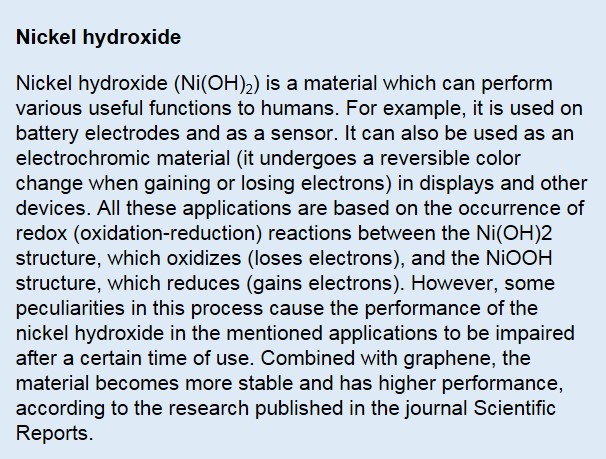 A recently published paper in the journal Scientific Reports, from the Nature group, reports a study carried out in universities of the state of Paraná (Brazil) on a material based on nickel hydroxide Ni(OH)2 – a composite of great technological interest [See box]. The group of authors developed an innovative method to fabricate a material based on nickel hydroxide graphene and nanoparticles, prepared thin films with this material and demonstrated the efficiency of these films when used as rechargeable battery electrodes, glycerol sensors and electrochromic materials.
The work was carried out within the doctoral research of Eduardo Guilherme Cividini Neiva, under the guidance of Professor Aldo José Gorgatti Zarbin, in the Chemistry Post-Graduation Program of the Federal University of Paraná (UFPR). Neiva began his research on nickel nanoparticles during his undergraduate years, guided by Professor Zarbin. In the master’s program, still with Zarbin, he developed a preparation route of nickel metal nanoparticles for electrochemical applications. After completing the master’s program, Neiva and Zarbin set out to continue the research in Neiva’s doctorate, including graphene in the preparation of nickel metal based nanoparticles to obtain nickel and graphene nanocomposites with different properties. “Most of my scientific interests focus on the preparation of materials with carbon nanostructures, such as nanotubes and graphene,” states Professor Zarbin, who is the corresponding author of the article in Scientific Reports.
They were surprised by the first laboratory results. In the presence of graphene oxide (as a precursor of graphene in the preparation of the material), the process took a different course. At that time, Neiva and Zarbin saw the potential of these particularities: if well understood, they could be controlled and used to prepare nanocomposites, not only of nickel metal, but also of nickel hydroxide, which would open up new application possibilities. “There is a phrase by Louis Pasteur I like very much, which applies perfectly in this case: “Chance favors the prepared mind,” declares Zarbin.
Based on this, student and advisor created a simple and direct process for the fabrication of graphene and nickel hydroxide nanocomposites. In this innovative process, both components are synthesized together in a one-step reaction. Using this technique, Neiva manufactured the nanocomposites. Pure nickel hydroxide samples were also produced in order to compare them with the nanocomposites.
The samples were studied through a series of techniques: X-ray diffraction, Raman spectroscopy, Fourier transform infrared spectroscopy (FT-IR), thermogravimetry, field emission scanning electron microscope (FEG-MEV), and also by means of transmission electron microscopy (TEM) images carried out by Professor Marcela Mohallem Oliveira, from the Federal Technological University of Paraná (UTFPR). The comparison between the two materials was favorable to the nanocomposite. “Graphene played a key role in the stabilization of particles at the nanometer scale, increasing the chemical and electrochemical stability of the nanoparticles, and increasing the conductivity of the material, which is fundamental for an improvement in the desired applications,” acknowledges Aldo Zarbin.

The next stage consisted of
processing the nanocomposites and the nanoparticles of pure nickel hydroxide to obtain thin films, a format that allows using them in the desired applications. “The deposition of materials in the form of films, covering different surfaces, is a great technological challenge, even greater when dealing with multicomponent materials and insoluble, infusible and intractable materials (all characteristics of the material reported in this article)”, explains Zarbin.
To overcome this challenge, Neiva used a processing route, known as liquid/liquid interfacial method, developed in 2010 by the research group led by Zarbin, the Materials Chemistry Group of UFPR. This route, besides simple and cheap, explains Professor Zarbin, allows depositing complex materials in the form of homogeneous and transparent films on various types of materials, including plastics. “The route is based on the high energy at the interface of two immiscible liquids (e.g., water and oil), where the material is initially stabilized to minimize this energy, allowing its subsequent transfer to substrates of interest,” he explained.
With the nanocomposites, Neiva obtained thin transparent films of about 100 to 500 nm in thickness, with nanoparticles of about 5 nm in diameter, distributed homogeneously on the graphene sheets. The pure nickel hydroxide, however, generated films formed by porous spherical nanoparticles of 30 to 80 nm in diameter, distributed heterogeneously, forming agglomerates in some regions.
In the final phase of the work, the films deposited on glass and indium tin oxide were tested in three applications, in which the nanocomposite performed better than pure nickel hydroxide. As a material for rechargeable alkaline battery electrodes, the nanocomposite exhibited high energy and high power – two positive points that are not easily found in the same material. The nanocomposite also showed good performance as an electrochemical sensor. In fact, experiments designed by Professors Márcio Bergamini and Luiz Marcolino Jr, also from UFPR, showed that the nanocomposite is a sensitive sensor of glycerol (a compound known commercially as glycerin and used in several industries). Finally, the nanocomposite acted as an efficient electrochromic material. With these characteristics, the films of the UFPR group have a chance to leave the laboratory and be part of innovative products. “This depends on partners who are interested in scaling the method and testing it on real devices,” says Zarbin.
For now, in addition to scientific articles such as the one published in the journal Scientific Reports, the work generated several patents, both on the deposition method of thin films and on their applications in gas sensors, transparent electrodes, photovoltaic devices and catalysts. “And we have now developed a flexible battery, which was only possible thanks to the film deposition technique we developed,”, adds Professor Zarbin.
The work, which was developed within the macro projects “INCT of carbon nanomaterials” and “Nucleus of Excellence in Nanochemistry and Nanomaterials”, received funding from the federal agencies Capes and CNPq, and the Araucária Foundation, an agency for scientific and technological development of the state of Paraná.

The search for the materials that are most suitable for performing certain tasks maybe exists since the dawn of humanity. In this search, on the opposite end to the trial and error method, there is the combinatorial approach, which aims to increase the efficiency of the process of discovering or producing materials. This approach is based on the screening of large amounts of materials with compositions slightly different one another, using databases, rapid synthesis and characterization techniques, simulations, robots and other tools. The combinatorial approach has been applied to the pharmaceutical industry since the 1990s to identify new and useful compounds, and it also has its place in the field of Materials Science and Engineering.

During the XIV SBPMat Meeting, Professor Ichiro Takeuchi will give a plenary talk on the combinatorial approach to materials discovery – an issue that is part of his daily life. Takeuchi is a Professor of the Materials Science and Engineering Department at the University of Maryland, in the United States, since 1999. In this institution, he leads the Combinatorial Synthesis and Rapid Characterization Center and the Keck Lab for Combinatorial Nanosynthesis/ Multiscale Characterization. He is a Visiting Professor at the Tokyo University of Science since 2010. He is also member of the Executive Committee of the Forum on Industrial & Applied Physics from the American Physical Society (APS).
Takeuchi graduated with a Degree in Physics in 1987 at the California Institute of Technology (Caltech). For four years he worked in Japan at the microelectronics research laboratories of the NEC Corporation, to later return to the United States. In 1996, he earned his Ph.D. at the University of Maryland. Then, he went to the Lawrence Berkeley National Laboratory, where he stayed until 1999 as a postdoctoral researcher. In 2004, he was the chairman of the Gordon Conference on Combinatorial and High-throughput Materials Science. In 2009, he founded a company dedicated to the development of materials and systems for applications in the field of energy, the Maryland Energy and Sensor Technologies, LLC.
Ichiro Takeuchi was a Visiting Professor at universities in Japan and Germany. He has received awards and distinctions from the National Science Foundation (Career Award), the Office of Naval Research in the US (Young Investigator Program Award) and the University of Maryland, among other institutions. The scientist, whose H index is 40, according to Google Scholar, is the author of over 180 papers, with more than 5,900 citations, and a book on the combinatorial synthesis of materials.
What follows is a brief interview with this plenary speaker.
SBPMat newsletter: – Help us to visualize how the combinatorial research is performed. For instance, choose an example of a material created in your laboratories with this approach, and outline the “step-by-step”.

Ichiro Takeuchi: – We do thin film based combinatorial materials research. The goal is to carry out rapid screening of previously unexplored compositional landscape in order to discover new materials with enhanced physical properties. We make wafers or chips where there are large composition variations in deposited thin films. Sometimes the thin films are separated into different pads, and sometimes it is one continuous film with changing composition across the wafer. We want the variation to be as large and diverse as possible, so that we can map large compositional variation in a single experiment. We then take different characterization techniques to carry out rapid screening of various physical properties. For example, right now, we have a project to search for new permanent magnet materials. For this, we use techniques such as scanning SQUID or scanning magneto-optical Kerr effect measurements. These measurements can be used to map magnetic properties of all the compositions on a single wafer. These wafers and chips are called combinatorial libraries. We also do a lot of structural characterization. For this purpose, we often go to synchrotron beamlines. At such locations, because of the large beam flux, we are able to carry out x-ray diffraction of the entire wafer very quickly. Right now, we can scan 200-300 spots in 2 hours.
SBPMat newsletter: – In your opinion, what are your most significant contributions in the field of combinatorial materials science? Please explain them, very briefly, and share references from the resulting articles or books, or comment if these studies have produced patents, products, spin-off companies etc.

Ichiro Takeuchi: – Over the years, we have carried out combinatorial investigation on a variety of topics in the general field of functional materials. They include superconductors, shape memory alloys, magnetosrictive materials, ferroelectric and dielectric materials to name a few. In carrying out such experiments, we have had to develop and establish techniques to effectively implement the strategies. We have indeed discovered a number of new compounds. For instance, working together with theoretical colleagues, we have found shape memory alloys with long fatigue lives. I have patents on a number of low-loss dielectric materials as well as novel piezoelectric materials. Many groups are now doing follow-on work on a lead-free morphotropic phase boundary piezoelectric material we found a number of years ago. In addition to the materials that were discovered, we have established combinatorial strategies as a technique to rapidly delineate composition-structure-property relationships in different materials systems. We have recently published a comprehensive review article. It is: “Applications of high throughput (combinatorial) methodologies to electronic, magnetic, optical, and energy-related materials,” Journal of Applied Physiscs 113, 231101 (2013) by Martin L. Green, Ichiro Takeuchi, and Jason R. Hattrick-Simpers.
SBPMat newsletter: -If you wish, leave a message or an invitation to your plenary talk to the readers who will attend the XIV SBPMat Meeting.
Ichiro Takeuchi: – The notion of search and discover is central to materials research. The combinatorial methodology is the natural counterpart to the concerted efforts in theoretical design of materials taking place around the world. By effectively coupling theory with high-throughput experimentation, we can really accelerate the rate at which new materials are discovered. I will present a mode of research we call “integrated materials engine” where theory and experiments are woven together and built on a flexible database and data management platform.

More:
Paper: Annealing effects on the microwave linewidth broadening of FeCuNbSiB ferromagnetic films. Alves, M.J.P.; Gonzalez-Chavez, D. E.; Bohn, F.; Sommer, R. L. Journal of Applied Physics. 117, 123913(2015) DOI: 10.1063/1.4915330.

A team of scientists from the Brazilian Center for Research in Physics (CBPF) and the Federal University of Rio Grande do Norte (UFRN) conducted a study on magnetic properties of thin films made of a nanocrystalline material (i.e, formed by nanometric grains) type FINEMET. The conclusions of this scientific research can help produce high quality magnetic materials suitable for use in small-sized devices, such as magnetic random access memories (MRAMs) or nano-oscillators. Results of the study were reported in a recent article in the Journal of Applied Physics.
FINEMET type materials are alloys based on iron (Fe), silicon (Si) and boron (B) with small additions of copper (Cu) and niobium (Nb). They have very good magnetic properties when they are produced by rapid cooling followed by annealing. However, there is not yet an established route that allows obtaining the material having these properties in the form of thin films, which are better suited for miniaturized applications.
In the work of the Brazilian team, magnetic thin films FeCuNbSiB were synthesized at CBPF by scientists from UFRN and CBPF. Samples of the film were analyzed using various techniques such as grazing incidence X-ray diffraction, magnetometry and, in particular, broadband ferromagnetic resonance (FMR). “We explored this technique to the limit,” said Rubem L. Sommer, one of authors of the Journal of Applied Physics paper. “It is powerful and has allowed the study of nanostructured materials with great efficiency,” added the CBPF researcher. Sommer and his team have been contributing to the development of broadband ferromagnetic resonance technique since 2011.
The ferromagnetic resonance technique is used to study the magnetization of the material, measuring the amount of electromagnetic radiation in the microwave range that a particular material absorbs. In the conventional version of this technique, explains Sommer, this absorption is measured at a fixed frequency, and the external magnetic field is varied to tune the equipment in resonance. In the microwave range, the frequency may be between 300 MHz and 300 GHz, and 1 Hz equals 1 oscillation per second. “In the case of ferromagnetic resonance broadband, we scan frequency and the external field, making a direct mapping of the material dispersion relation,” explains Sommer.

Based on the combination of the films analyses obtained by the various techniques, the team of scientists unveiled the mechanisms that are responsible for broadening the ferromagnetic resonance linewidht in the material. “The thinner the resonance line, the higher the quality of the material for applications”, said Sommer. The scientists could conclude that the residual stresses (those who remain in the materials after the elimination of their causes) were causing the enlargement of the resonance linewidth, and that annealing reduced these tensions.
The study reported in the article was funded by Brazilian agencies CNPq and CAPES and was developed mainly in the doctoral research of Marcos Alves held in CBPF and recently defended. The doctoral dissertation of Diego González-Chávez, defended in 2013, was also important for the article, as it allowed the successful development of the broadband FMR technique.
The authors of the article are part of a larger network of collaboration that includes, in addition to researchers from CBPF and UFRN, contributors from PUC-Rio and the federal universities of Santa Maria (UFSM) and Rio Grande do Sul (UFRGS), says Sommer. “I believe that this work, as well as the performance of a network spread over different institutions is a very positive aspect of the current Brazilian scientific and technological research reality”, he said. The network develops research on nanostructured materials and magnetic devices for use at high frequencies. “Our research has always a double bias: basic research to understand the phenomena and application development,” said Sommer.
Scheme of ferromagnetic resonance equipment used in broadband research. The Kepco source feeds the magnetizing circuit (Helmholtz coils) and the signal is measured with a vector Network Analyzer (VNA). The sample is placed on a coplanar waveguide with micrometric dimensions.
Results typical broadband of FMR: microwave absorption curve (color) depending on the field and frequency.
 Israel Jacob Rabin Baumvol was born in Rio Grande do Sul, in the city of São Gabriel, in the last day of 1947. When he was a child, he moved to the city of Porto Alegre with his parents and siblings. When he was 19 years old, he entered the Federal University of Rio Grande do Sul (UFRGS) to study Physics. In the following years, in addition to participating in the political activity that occurred in the university against the existing military government, Baumvol dedicated a lot of effort to his studies, trying to reach the academic standard of the bachelor’s degree in Physics of the university. In 1971, he completed the graduation course – without honors, according to him. In the following year, he moved to the city of São Paulo to take a Master’s Degree in the University of São Paulo (USP), in Nuclear Physics and under the orientation of Professor Oscar Sala. In 1975, he returned to UFRGS to undertake his Doctorate, with orientation of Professor Fernando Zawislak, studying composites of perovskite structures. During the doctorate, he became a professor at UFRGS. In 1977, he defended his thesis. For the postdoctoral course, Baumvol chose an institution of industrial research in England, today known as Harwell campus. There, between 1979 and 1981, he worked with techniques of ionic implantation and its applications, mainly the plasma immersion ionic implantation (PIII), and he took part in research contracts with large companies. Due to his expertise in PIII, Baumvol entered the world of the materials for microelectronics, an area in which he made significant scientific contributions and obtained international reputation.
In the United States, Israel Baumvol was an invited researcher of the IBM research center from 1984 to 1988 and, from 1998 to 1999, of the Bell Laboratories, belonging to company Lucent. In France, between 1992 and 1996, he was a visiting professor at the Université Pierre et Marie Curie and at the Université Paris Diderot (Paris 7). In 1997, after coming first in a public entrance examination, he was nominated full professor at Paris 7, but he did not take over the position to stay in UFRGS. From 1995 to 1996, he was a guest professor of the Ruhr Universität, in Germany.
Baumvol was also coordinator of international events held outside Brazil. In 2000 and 2005, he was coordinator (chairman) of international symposia of Physical-Chemistry of silicon oxide and silicon – silicon dioxide interface, organized by the Electrochemical Society. In 2001, he coordinated the International Workshop on Device Technology of the Materials Research Society (MRS), held in Porto Alegre. In 2004, he was meeting chair of the MRS Spring Meeting & Exhibit, that occurs annually in San Francisco (United States).
In 2003, after retiring from his position of full professor of UFRGS, he led the creation of the Materials Science and Engineering Potgraduation Program of the University of Caxias of Sul (UCS), near 130 km far from Porto Alegre, and he was coordinator and researcher of the program until 2014.
From 2002 to 2003, Baumvol presided the Research Support Foundation of the State of Rio Grande do Sul (FAPERGS). More recently, between 2011 and 2013, he was vice-coordinator of the Materials Department in Capes (a federal agency for higher education improvement). Baumvol also coordinated big projects in the Materials segment, such as the first National Network of Research in Nanostructured Materials (2001-2005) and the National Institute of Surface Engineering (2009 to 2010).
Throughout his scientific career, Israel Baumvol has carried out research in subjects related to ionic implantation, thin layer physics and surface modification, in addition to materials for microelectronics.
Baumvol holds the highest productivity level scholarship in CNPq, the Brazilian federal science council. He has authored over 270 peer-reviewed articles, besides books and book chapters. His scientific production has approximately 3,000 citations. He acted as advisor in about 30 Master’s Degree and Doctorate dissertations.
In 2000, he was chosen Prominent Researcher by FAPERGS; in 2010, he was nominated Commander of the National Order of the Scientific Merit by the Presidency of the Brazilian Republic and in the following year, he was named Professor Emeritus by UFRGS. In May of this year, the “Professor Israel Baumvol Microscopy Center” was inaugurated in UCS.
Here is an interview with the scientist.
SBPMat newsletter: – Tell us what led you to become a scientist and to work in subjects of the Materials field.
Israel Baumvol: – It was the junction of three factors. The first one was the desire to use my knowledge one day to be able to contribute to the progress of the country and its citizens. This desire was developed through reading and great political participation during the graduation course. However, seeing as in Porto Alegre the tradition of basic research was very strong and there was nobody working in applied physics, I had a strict academic formation, that was very good for my future. The second factor was my post-doctorate, for which I chose an institution of industrial research, in England. I went there in 1979 to learn ionic implantation, because the institution was a pioneer in this method. There, I became acquainted with ionic implantation, specially its applications, such as reduction of the friction in metallic components (for example Ti-Al alloys) by means of implantation of species and heavy ionic composites, increase of the resistance to wear and corrosion of steel by nitriding, oxinitriding and nitrocarburizing using the method of ionic implantation by immersion in plasma (PIII). At that time, they were constructing there the first industrial-scale reactor of PIII, with a volume of approximately 30 m3, which was later spread throughout the world, including by companies that manufactured these reactors, such as Eaton and several others, including two companies in Brazil. This environment of applied physics fascinated me due to its possibilities. I participated in many research contracts, such as the one about bone prosthesis for a Japanese manufacturer, another about turbine blades for Rolls-Royce and another on cut blades for the future electric shavers project for Philips. These projects, in addition to fascinating me, had a component that for me was romantic: they were confidential projects. The third and last factor occurred by the end of my post-doctorate. I went to a congress in Germany, where I gave a 50-minute lecture, something very difficult nowadays, when the lectures only last about 20 minutes. When I finished speaking and answering questions, there was a coffee break. Dr. James F. Ziegler came up to me, introduced himself and gave me his business card, in which it was written “Research Director, Thomas J. Watson Research Center, IBM”. He invited me to go there because, during my lecture, he thought that the PIII method could solve a serious problem that IBM had with hard drives. Yet again, the siren song of a confidential project. I accepted the invitation and, for some years, during winter and summer vacations, three to four months per year, I went to IBM – Yorktown. There, I got in touch with something unusual for me, the silicon technology, which was just being born. That was yet another allure and my mind was made, Materials Science and Engineering.
SBPMat newsletter: – What are, in your own evaluation, your main contributions to Materials field?
Israel Baumvol: – I worked in many different subjects in my professional activity, some of them mentioned above. I will highlight three of them. The first one was my participation in the beginning of the PIII technology, which is nowadays widely used in the whole world, also in Brazil, where there are at least four services of PIII processes of steel components for the metal-mechanics industry. The second one is my contribution, throughout ten years of work, to explore and to reach the physical limits of silicon oxide as gate dielectric in the metal oxide semiconductor (MOS) technology. I formed a network of cooperation with academic laboratories in four different countries and with industrial laboratories, including IBM, Motorola, Texas Instruments, Bell-Lucent. We reached the physical limit, 1 nm. From there, the entire network started to work on a substitute for silicon oxide, which was the first change in the MOS technology, after forty years. There was a convergence for hafnium oxide and, eventually, certain hafnium-based double oxides. This material stood out, allowing an increase of processing speed and today it is used as gate oxide in advanced processors. It allowed the continuity of the Moore Law, which was threatened. This research segment led to the formation of a golden generation of PhDs, all around gate oxide, which is a crucial subject for the micro and nanoelectronics. Many of them are acting professionally in industrial companies, in technology of silicon and in other activities. Finally, I highlight the creation of a research environment in Materials Science and Engineering and of a post-graduate program in this segment. I started this activity with only one element: Caxias do Sul and its environs possess a large number of industrial companies, small, average and large companies needing research and human resources qualification. Only this, nothing more. Then, from nothing, I gathered some young high-qualified doctors and built the desired research environment, with many excellent laboratories and a very respectable post-graduation program. The impact on the industrial context of the region is notable and very recognized.
Bulletin of SBPMat: – Leave a message for our readers who are initiating their careers of scientists.
Israel Baumvol: – Follow your heart and not convenience. Take advantage of the doctorate, because this is the best time of the career: creative research and free from administrative responsibilities. Do not hesitate in showing your ideas. New ideas are not necessarily bad ideas. Use your post-doctorate to get in touch with the new and the unknown. Do not look for a place that works with the same subject of your doctorate research. Do not hesitate in changing the field, this is very stimulant and constitutes an important factor of individual progress. I pity the professionals who continue working in the subject of their doctorate theses, ten or twenty years after the conclusion. Applied research can very be good research. Get rid of preconceptions, it does not matter if the research is fundamental, or applied or directly industrial. What counts is quality. The only difference is between good quality research or bad quality research.
The scientific paper by members of the Brazilian community in Materials research featured this month is:
Fernando Stavale, Niklas Nilius, and Hans-Joachim Freund. STM Luminescence Spectroscopy of Intrinsic Defects in ZnO(0001̅) Thin Films. J. Phys. Chem. Lett., 2013, 4 (22), pp 3972–3976. DOI: 10.1021/jz401823c.
Luminescence measurements to identify defects in zinc oxide thin films.
Zinc oxide (ZnO) is a very common material in everyday life. It can be found in screws, sunscreen, catalyzer for methanol synthesis and sophisticated optoelectronic devices, such as computer flexible screens, to name just a few. However, in order to enable some promising applications, such as transistors and new devices, it is important to control electrical properties of this semiconductor material, which are related to specific defects in its atomic structure.
Within this context, three scientists from institutions in Germany and Brazil identified specific defects in zinc oxide films through an original approach, taking advantage of luminescence capability (emission of light not resulting from heat) of zinc oxide. Researchers prepared zinc oxide thin films with different types and amounts of specific defects. Systematically, scientists measured luminescence of each film and, thus, they managed to relate peaks on the measurements with various types of defects in crystal nets. The results of this study were published in periodical The Journal of Physical Chemistry Letters (JPCL).
“In this study, we developed extremely high quality thin films of zinc oxide and we altered the amount of specific defects using thermal desorption, photo-desorption induced by laser and reduction by treatment in hydrogen controlled environment” – says Fernando Stavale, researcher for Centro Brasileiro de Pesquisas Físicas (CBPF), who signs the article as main author.
Characterization technique
In order to make the experiments, scientists used a scanning tunneling microscope (STM) in ultra high vacuum with a few peculiarities designed to generate luminescence, collect the emitted photons and obtain the measurements (spectrum) of luminescence. With this configuration, the STM is known as photon-scanning tunneling microscope. According to Stavale, one of the main scientists in the field of development and application of this technique is Professor Niklas Nilius, correspondent author of the JPCL paper, with whom Stavale has directly worked for three years during his post-doctoral research at Fritz-Haber Max-Planck Society, in Berlin, specifically at Physico-chemical Department led by Professor Hans-Joachim Freund, last author of the JPCL article. “The photon-scanning tunneling microscope has been employed in unprecedented manner to characterize metallic acids at the department directed by Professor Freund” – says Stavale. “The technique is still underused in Brazil and it is an essential part of the projects I develop with my research team at CBPF, situated in Rio de Janeiro” – he adds.
One of the most important features in photon-scanning tunneling microscopy is the use of electrons which are emitted by the tip of the STM to excite samples and, in the case of zinc oxide, to generate the desired luminescence. This phenomenon of emitting light generated by the impact of electrons over the material is called cathodoluminescence.

Experiment scheme in which the tip of the tunneling microscope can be observed, in the photo, exciting the zinc oxide film. The graph shows a spectrum of the oxide cathodoluminescence. At the back , the tunneling microscopy image of a zinc oxide film, with density of 20 layers (~5 nm) shows monoatomic steps and specific defects in the film’s surface. Vacancies of oxygen and zinc, specific defects, correspond to the areas indicated by arrows. The dark areas with hexagonal shape correspond to the areas where the film is noncontinuous, with depth of up to eight atomic layers.
This systematic work allowed scientists to infer that some peaks of luminescence of zinc oxide are due to defects such as vacancies of oxygen and zinc (dots in the lattice containing “vacancies”, instead of the expected oxygen and zinc atoms). “These specific defects are related to electrical properties often observed in zinc oxide, known as n-type doping” – Stavale adds.
The context of the work
The experiments of the JPCL article were conceived and conducted by Brazilian national Fernando Stavale in 2012, during his last year of post-doctoratal research with the group led by Professor Nilius, at Fritz-Haber of Max-Planck Society. Stavale joined the group in 2010 with financial support from Humboldt Institute in Germany. “For three years we have investigated for the first time the role of several dopants, such as chromium, europium and lithium in zinc and magnesium oxides, combined with ultra-thin films, raised in ultra-high vacuum with tunneling microscopy and local cathodoluminescence” – says Stavale about his post-doctoral studies.
The interpretation of results and the JPCL article redaction were performed in 2013 when Fernando Stavale became a CBPF researcher and Niklas Nilius became a Professor at University of Oldenburg, Germany.
Neste mês, a seção “Artigos em destaque” do boletim traz a divulgação do trabalho vencedor do Prêmio Bernhard Gross ao melhor trabalho de estudantes apresentado no XII Encontro da SBPMat:
Self-organized 2-D Ni particles deposited on titanium oxynitride coated Si crystal sculpted by low energy ion beam. M. Morales, R. B. Merlo, R. Droppa Jr, and F. Alvarez.
Texto de divulgação:
Silício revestido para promover a auto-organização de partículas metálicas
Uma pesquisa de doutorado que está sendo desenvolvida no Instituto de Física “Gleb Wataghin”, da Unicamp, gerou uma contribuição à engenharia de superfícies ao propor um método simples para promover a formação de estruturas auto-organizadas sobre superfícies nanoestruturadas. Apresentada no XII Encontro da SBPMat pela doutoranda Mónica Morales Corredor, a pesquisa mereceu o Prêmio Bernhard Gross ao melhor trabalho do evento.
No trabalho, os pesquisadores descrevem a realização de três passos sucessivos. Num primeiro momento, um substrato de silício (Si) é esculpido mediante bombardeamento com íons de xenônio (Xe+), formando um padrão regular de sulcos e ondulações. Em seguida, essa superfície ondulada é revestida com um filme de oxinitreto de titânio (TiNxOy) que acompanha os relevos da lâmina de silício. Finalmente, partículas de níquel (Ni) são depositadas sobre o filme usando a técnica de pulverização catódica por feixe de íons. De maneira espontânea, as partículas se organizam num padrão que lembra uma malha ou rede de pesca.

O tema das superfícies nanoestruturadas combinadas com arranjos de partículas metálicas tem sido alvo de estudos pelas suas possibilidades de aplicação para fins ópticos, magnéticos ou catalíticos, como por exemplo, no crescimento de nanotubos de carbono. Nesse contexto, um dos principais méritos ou novidades do trabalho premiado é o uso do filme de oxinitreto de titânio. “Ele preserva as nanoestruturas geradas pelo bombardeamento iônico e atua como barreira à difusão superficial das partículas metálicas”, diz Mónica. No trabalho apresentado no encontro, além de descreverem os passos necessários para a fabricação do sistema, os autores discutem os processos de difusão e nucleação envolvidos na formação dessa rede de partículas regularmente distribuídas.
A estudante premiada
Mónica Morales Corredor, primeira autora do trabalho vencedor, tem graduação, mestrado e doutorado (este último, em curso) em Física. “O fato de eu escolher a Física como carreira já implica um interesse por querer entender a natureza, e a pesquisa faz parte desse entendimento”, comenta Mónica, que trabalha com Materiais desde a graduação.
De nacionalidade colombiana, a estudante se formou em seu país de origem e depois veio para o Brasil para fazer o mestrado, no qual estudou o efeito das superfícies no crescimento de nanotubos de carbono. “Depois de acabar o mestrado, vi que ainda faltava muito por entender e por trabalhar nesse tema, motivo pelo qual decidi continuar com meu doutorado, ainda na mesma área e com o mesmo orientador, o professor Fernando Alvarez”, relata Mónica.
O Prêmio Bernhard Gross
Homenagem a um dos pioneiros da pesquisa em Materiais no Brasil, o professor Bernhard Gross, o prêmio foi instituído pela SBPMat para promover e reconhecer a participação de jovens no estudo da ciência e tecnologia de Materiais ao selecionar os melhores trabalhos de estudantes de graduação e pós-graduação apresentados nos encontros anuais da sociedade. De acordo com os professores José Alberto Giacometti e Julio Sambrano, coordenadores do XII Encontro da SBPMat, o prêmio deve incentivar a melhora crescente na qualidade dos resumos submetidos e no preparo dos alunos para apresentar os painéis.

Prêmios Bernhard Gross 2013
No XII Encontro da SBPMat, foram selecionados dentro do Prêmio Bernhard Gross os melhores trabalhos de onze simpósios e, entre eles, o melhor trabalho de todo o evento. Os melhores trabalhos dos simpósios foram escolhidos pelas comissões julgadoras montadas pelos organizadores de cada simpósio. Para a seleção do melhor trabalho do evento, os membros de todas as comissões se reuniram. “Neste ano o júri teve muita dificuldade em escolher, pois o evento teve um número muito grande de excelentes trabalhos”, diz o professor Roberto Faria, presidente da SBPMat.
A cerimônia de premiação ocorreu durante a solenidade de encerramento do encontro, no dia 3 de outubro. O melhor trabalho do evento recebeu mil reais da empresa Shimadzu, patrocinadora do Prêmio Bernhard Gross 2013. Veja a relação dos trabalhos premiados:
Melhor trabalho do XII Encontro da SBPMat: Self-organized 2-D Ni particles deposited on titanium oxynitride coated Si crystal sculpted by low energy ion beam, M. Morales, R. B. Merlo, R. Droppa Jr, and F. Alvarez. Trabalho apresentado no simpósio L (Surface Characterization: Techniques and Applications).
Melhor trabalho do simpósio A (Sol-Gel Materials: From Fundamentals to Advanced Applications): Impedance electrical immunosensor for hepatitis C diagnostics based on biorecognition between the antigenic peptide NS5A-1 and the antibody anti-HCV. Marli Leite de Moraes, Alem-Mar Bernardes Gonçalves, Lais Roncalho Lima, Fernando Vieira Paulovich, Osvaldo Novais Oliveira Jr and Sidney José Lima Ribeiro.
Melhor trabalho do simpósio B (Inorganic Thin Films – Methods and Applications): Improvement of the wear properties of a diamond-like carbon film coated on ultrahigh molecular weight polyethylene for biomaterials. Jéssica Pereira dos Santos and Sérgio Camargo.
Melhor trabalho do simpósio C (Synthesis and Properties of Nanometric Materials): Cytotoxicity and Genotoxicity Evaluations of Nitric Oxide Donor Superparamagnetic Iron Oxide Nanoparticles. Amanda Franco Ludescher, Renata de Lima, Jhones Luis Oliveira, Ana Carolina Ferrarini, Amedea Barozzi, Seabra and Paula Silvia Haddad.
Melhor trabalho do simpósio D (Materials and Devices for Renewable Energy, Sustainability and Environment Protection): Study of the recovery and recycling of tailings from the concentration of iron ore for the production of ceramic aiming at sustainability. Fabiane Leocádia Silva, Fernando Gabriel Araújo, Fernando Leopoldo Kruger, Ana Paula Silva and Rodrigo Claudiano Gomes.
Melhor trabalho do simpósio E (Structure- properties relationship of advanced metallic materials): Deformation and Recrystalization of a trip/twip steel with 17% Mn and low C. Mirele Oliveira, Sara Ferreira de Dafé.
Melhor trabalho do simpósio F (Organic Electronics and hybrids: materials and devices): A facile combination of electroluminescence and photoluminescence properties to produce white light based on polymeric light-emitting diodes. Fernando Junior Quites, Teresa Dib Zambon Atvars and Gregorio Couto Faria.
Melhor trabalho do simpósio G (Molecular Modeling Materials Science): Hydrogen bonding of N-methylformamide with acetone. Glauco Garrido Almeida and João Marques Cordeiro.
Melhor trabalho do simpósio H (New Trends in Biomaterials and Nanomaterials Applied to Biosystems): Magnetic nanoparticles coupled with β-cyclodextrin as a delivery system for doxorubicin. Amanda Watanabe Paraguassú, Célia Machado Ronconi and Maria Domingues Vargas.
Melhor trabalho do simpósio N (Materials Education Symposium): An integrated project-based course for teaching of biomaterial biocompatibility to undergraduate students. Daniela Costa Silva, Juliana Alves Côrtes, Róber Freitas Bachinski, Carolina Nascimento Spiegel and Gutemberg Gomes Alves.
Melhor trabalho do simpósio O (Science, Engineering, and Commercialization of Next Generation of Industrial, Electronic and Biomedical Devices): Exploiting graphite-epoxy composite as electrode material for bioelectroanalysis. André Luiz Maia Azevedo, Renato Soares de Oliveira, Eduardo Ariel Ponzio, Juan Manuel Pardal and Felipe Silva Semaan.
Melhor trabalho do simpósio P (Advances in New Materials): Facile control of PFP morphology (glassy and α phases) in silicone-based polymer hosts. Fernando Junior Quites, Raquel Aparecida Domingues, René Alfonso Nome, Guilherme Ferreira Ferbonink and Teresa Dib Zambon Atvars.
Fotos de alguns dos premiados na cerimônia:


