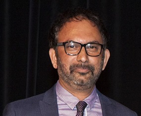
Despite all the knowledge on nanotechnology generated over the last few decades, applying nanomaterials to commercial products can still be a difficult task. At the XVI B-MRS Meeting, Professor Pulickel Ajayan, one of the world’s references in nanomaterials and nanostructures, will shed light on this problem. In the plenary lecture he will address in Gramado on the morning of September 14, Ajayan will discuss some challenges of the application of nanomaterials (particularly those of two dimensions) in systems and devices. He will address issues related to the synthesis, characterization and modification of these materials.
Ajayan and his collaborators have developed nanomaterials with diverse functionalities, applicable to fileds such as energy storage and conversion, catalysis, low consumption electronics, nanomedicine or environment care. Among his most famous contributions, are carbon nanotubes filled with molten material acting as nanowire moulds (1993); nanobrushes made of carbon nanotubes, highlighted by Guinness World Records as the smallest ones (2005); the paper battery, made of cellulose and nanotubes (2007); the ultra-dark nanotube carpet, which reflects only 0.045% of light (2008), and a reusable sponge of nanotubes capable of absorbing oil dispersed in water (2012).
Professor and director of the Department of Materials Science and Nanoengineering at Rice University (USA), Ajayan has exceptional publication metrics: a h index of 144 and more than 95,000 citations according to Google Scholar.
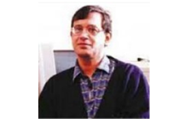
Pulickel Madhavapanicker Ajayan was born in 1962 in India, in a small town in the southern state of Kerala. He attended primary school there and then went to the state capital, to a high school that aroused his enthusiasm for learning, his curiosity, and his interest in science.
In 1985, Ajayan graduated in Metallurgical Engineering at Banaras Hindu University (BHU), located in northeastern India and then went on to do a PhD in Materials Science and Engineering at Northwestern University (USA). At that moment, he began to penetrate nanotechnology. In 1989, he defended his PhD thesis about very small gold particles that, some years later, would begin to be called “nanoparticles”.
In 1990, he moved to Japan to pursue a postdoctoral stage at the Fundamental Research Laboratory of the NEC Corporation, where he remained until 1993 in the group that was responsible for a series of seminal studies on carbon nanotubes – including the “discovery” of these nanomaterials, attributed to Sumio Iijima in 1991. During his postdoc, Ajayan obtained important results on the synthesis of nanotubes in large scale and on the filling of nanotubes with other materials.
From Japan, he went to France where he worked as a researcher at the Solid Physics Laboratory of the Université Paris-Sud for two years. Then he went to Germany, where he worked for a year and a half at the Max-Planck-Institut für Metallforschung. In 1997, he moved to the United States to become an assistant professor at the Rensselaer Polytechnic Institute (RPI), the nation’s oldest university of technological research, located in the state of New York. At RPI, he was the Henri Burlage chair Professor in Engineering and worked in the nanotechnology research group.
In 2007, he left RPI and joined the faculty of the Department of Mechanical Engineering and Materials Science at Rice University to be the Benjamin M. and Mary Greenwood Anderson professor of Engineering. In 2014, he also held the founding chair of the Department of Materials Science and NanoEngineering.
Currently, in addition to teaching and leading a research group of about 40 members at Rice University, Ajayan travels a lot, whether to share his knowledge on nanotechnology (he has delivered more than 350 invited lectures and has held visiting professor positions at universities around the world), or to take care of his scientific collaborations. In addition, Ajayan has acted on the boards of several journals, startups and international conferences of the materials and nanotechnology field.
The scientist has received important awards from a number of institutions including the Royal Society of Chemistry (UK), Alexander von Humboldt Foundation (Germany), Materials Research Society (USA), Microscopic Society of America (USA). He also received distinctions of numerous universities around the world, including the doctorate honoris causa by the Université Catholique de Louvain (Belgium). He is an elected member of the Royal Society of Chemistry (UK), American Association for the Advancement of Science (AAAS), and the National Academies of Sciences of India and Mexico, among other scientific societies.
Here follows an interview with the scientist.
B-MRS newsletter: – We would like you to choose some of your contributions to nanotechnology, describe them briefly, and share the paper reference, if possible. Please choose:
– The one(s) you consider to have caused or will cause more social impact.
Pulickel Ajayan: – Several of our discoveries have commercial and social impact. In the past two decades some of the research highlights from our lab have been carbon nanotube arrays as extreme light absorbers (for thermo-photovoltaics), nanotube arrays as gecko-tapes, high conductivity carbon nanotube fibers, graphene oxide membranes for water filtration, carbon nanomaterials for energy storage, light weight polymer nanocomposites, development of two-dimensional materials for electronics and sensors, carbon based quantum dots as catalysis for example CO2 reduction etc.
– The one(s) that gave you more personal satisfaction.
Pulickel Ajayan: – One of the most exciting work was related to the conversion of carbon onions into diamond nanoparticles using electron irradiation. This work was done in collaboration with Prof. Florian Banhart when I was visiting as a post-doc at the Max Planck Institute for Metallforschung in Stuttgart in the mid-90’s. This work published in Nature magazine showed direct observation of graphite to diamond phase transition without application of any external pressure.
B-MRS newsletter: – Have any of your scientific/ technological contributions been transferred to a commercial product? If so, has this transfer occurred through patent licensing, start-up …?
Pulickel Ajayan: – Two start-up companies (Paper Battery Co. and Big Delta Systems) have come out of our work; both engage in unconventional energy storage technologies.
B-MRS newsletter – Leave an invitation to your plenary talk for our readers.
Pulickel Ajayan: – Nanotechnology is a paradigm changing approach on how we will be building materials of the future. It is at the core of bottom-up manufacturing and will impact several areas of future technologies. Our work in the past two decades have focused on creating nano-engineered materials with various types of nanoscale building blocks.
More information
On XVI B-MRS Meeting website, click on the photo of Pulickel Ajayan and see his mini CV and the abstract of his plenary lecture: http://sbpmat.org.br/16controter/home/