Click on the icon below to go to the web album with our photoreport of the event.
 |
| XIV SBPMat (B-MRS) Meeting – Rio de Janeiro, Sept 27 – Oct 1, 2015 |
Click on the icon below to go to the web album with our photoreport of the event.
 |
| XIV SBPMat (B-MRS) Meeting – Rio de Janeiro, Sept 27 – Oct 1, 2015 |
|
||||||||||||||||||||||||||||||||||||||||

Materials created by applying the state-of-the-art in materials science and engineering and nanotechnology can make light and other electromagnetic waves behave in an extraordinary way, becoming very useful for applications in several fields.
To talk about this issue in the XIV SBPMat Meeting, Professor Nader Engheta (University of Pennsylvania, USA) will be in Rio de Janeiro in the end of September. Engheta is a recognized world leader in research on metamaterials – man-made materials created through micro or nanoengineering, and capable of interacting with electromagnetic waves in ways not found in nature. Metamaterials can sculpt the waves in order to achieve unconventional light-matter interaction.
In Rio de Janeiro, Engheta will talk about extreme scenarios generated from metamaterials: light traveling at full speed through artificial structures, one-atom-thick optical devices, metamaterials that perform mathematical operations, miniaturized circuits – optical rather than electronic – composed by metamaterials, and structures with effective refractive index near zero.
In his childhood in Tehran (capital of Iran), Nader Engheta developed a special curiosity to understand phenomena related to waves. This curiosity propelled him to attend and get a BS degree in Electrical Engineering at the University of Tehran. In 1978, he came to the United States to pursue his post-graduate (master’s and PhD degrees), also in Electric Engineering, carried in the prestigious Caltech (California Institute of Technology), in the United States. In 1982, he got his PhD diploma from Caltech, with a dissertation in the field of electromagnetism. After a post-doctorate at the same institution, Engheta worked as a scientist in the industry for four years, working again with electromagnetism. Then he joined the faculty of the University of Pennsylvania in Philadelphia in 1987, and was swiftly promoted through the professorial ranks, and now he is the H. Nedwill Ramsey Professor of Electrical and Systems Engineering, with affiliations in the departments of Electrical and Systems Engineering, Physics and Astronomy, Bioengineering and Materials Science and Engineering.
Owner of an H number of 69 according to Google Scholar, Engheta has more than 21400 citations. Besides being author of 28 book chapters and numerous journal articles and conference presentations, Engheta is coeditor of the book “Metamaterials: Engineering and Physics Explorations”, released in 2006 by Wiley-IEEE publisher. In 2012, he chaired the Gordon Research Conference on Plasmonics.
His contributions to science and engineering have received important recognitions and distinctions from several entities, as the international society of optics and photonics, SPIE (“2015 SPIE Gold Medal”), the international union of radio science, URSI (“2014 Balthasar van der Pol Gold Medal”) and the international professional association of electric and electronic engineers, IEEE (“2015 IEEE Antennas and Propagation Society Distinguished Achievement Award”, “2013 Benjamin Franklin Key Award”, “2012 IEEE Electromagnetics Award”, “IEEE Third Millennium Medal”), among many other entities. He is also Fellow of six international scientific and technical organizations, namely, Materials Research Society (MRS), American Physical Society (APS), Optical Society of America (OSA), American Association for the Advancement of Science (AAAS), SPIE, and IEEE. Engheta also received several teaching awards. In 2006 the Scientific American Magazine selected him as one of the 50 Leaders in Science and Technology for his development of metamaterial-inspired optical nanocircuitry.
Here follows an interview with Professor Nader Engheta.
SBPMat newsletter: – In your opinion, what are your most significant contributions on issues related to the topic of your plenary lecture? Explain them very briefly and if possible, share references of resulting papers or books, or comment if these studies have produced patents, products, spin-off companies etc.
Nader Engheta: – I am very interested in light-matter interaction, and in my group we explore different methods in manipulating and tailoring interaction of waves with material structures, both in the optical as well as microwave domains. I am very excited about all the research topics my group and I have been working on. Some of these topics include (1) The optical metatronic nanocircuitry, in which we brought the notion of “lumped” circuit elements from electronics into the field of nanophotonics, developing a new paradigm in which material nanostructures may function as optical circuit elements. In other words, “materials become circuits” working with optical signals. In this way, nanophotonics can be modularized, in an analogous way as in electronics. This allows one to perform optical signal processing at the nanoscale, (2) Metamaterials that can do math: following our work on optical metatronics, we are exploring how properly designed materials (e.g., layered materials) can interact with light in such a way that one can do mathematical operations with light. In other words, we are exploring the following questions: Can materials be specially designed to perform analog processing with light at the nanoscale? As light propagates through such properly designed material structures, would the profiles of the output signals resemble the results of certain mathematical operations (such as differentiation or integration) on the profiles on the input signals? In other words, can we design materials for specific mathematical operations in order to do “photonic calculus” at the nanoscale? (3) The extreme scenarios in light-matter interaction: this may include extreme dimensionality, like graphene photonics as the one-atom-thick platform for light manipulation, extreme metamaterials in which material parameters such as relative permittivity and relative permeability attain near-zero values. This category of materials, which we have named epsilon-near-zero (ENZ), mu-near-zero (MNZ) and epsilon-and-mu-near-zero (EMNZ) materials, exhibit very interesting features in their response to electromagnetic wave interaction.
References:
SBPMat newsletter: – Help us visualize the metamaterials developed by your group. Please choose one of your favorite photonic materials and tell us, very briefly, its composition, its main properties and its possible applications.
Nader Engheta: – One of the structures developed by my group is the optical metatronic nanocircuits for mid-IR regime (from 8 to 14 microns), in which we properly tailored and constructed nanorods of Si3N4 with specific widths and thicknesses, separated by a specific gap. These arrays of Si3N4 nanorods function as collections of optical nanoinductors, optical nanocapacitors and optical nanoresistors in mid IR. We demonstrated that such structures behave as nanoscale optical circuits, with functionality analogous to electronic filters, but here these material structures operate in the mid IR regimes. We have shown how these structure operate as optical filters in the mid IR, offering exciting applications for future integrated optical devices and components.
Reference:
Later, in collaboration with my colleague Professor Cherie Kagan and her group at UPenn, we extended this work into the near IR regime (from 1 to 3 microns). In this case, we used the indium tin oxide (ITO) as the material of choice, with proper design and patterning of ITO nanorods. We also demonstrated that such ITO-based optical metatronic circuits function as an interesting platform for optical circuitry and filtering. This can have exciting possibilities in the silicon photonics.
Reference:
SBPMat newsletter: – If you want, leave a message or invitation to your plenary lecture to the readers that will attend the XIV SBPMat Meeting.
Nader Engheta: – One of the exciting features of doing science is the joy of search for unknowns and the thrill of discovery. I always believe that we should follow our curiosity and our passion for discovery. Also, in science and technology it is important to maintain the balance between the complexity and the simplicity in search for solutions to scientific inquiry.
More
[Paper: Assisted deposition of nano-hydroxyapatite onto exfoliated carbon nanotube oxide scaffolds. Hudson Zanin, Cintia M. R. Rosa, Noam Eliaz, Paul W. May, Fernanda Roberta Marciano and Anderson O. Lobo. Nanoscale, v. 7, p. 10218-10232, 2015. DOI: 10.1039/C4NR07317G]
In a study conducted by the Laboratory of Biomedical Nanotechnology (NANOBIO) from the Brazilian University of Vale do Paraíba (UniVap), in a partnership with scientists from the Brazilian National Institute for Space Research (INPE) and universities from Israel and the UK, a biomaterial was produced that advanced the understanding of some stages on the generation of bone tissue in vitro (out of the real biological context). The low cost material has the potential to be used to accelerate the regeneration of bone tissue in vivo – which may be useful in case of bone fractures, for example. The results of the study were recently published on the scientific journal Nanoscale, from the Royal Society of Chemistry.
In broad terms, the natural generation of bone tissue occurs when cells called osteoblasts produce the organic part of bones to later cover it with the inorganic part, the hydroxyapatite – chemical formula Ca5(PO4)3(OH). The natural deposition of hydroxyapatite is a biomineralization process (production of minerals by living organisms). The biomineralization is not yet fully understood, but its comprehension is of great importance for the development of applications aiming to create bone tissue or firm implants into bones.
“The paper contributes to the understanding of the precipitation process of carbonated hydroxyapatite in vitro, for short amounts of time, over three-dimensional surfaces based on nanohydroxyapatite, vertically aligned carbon nanotubes and graphene”, says Professor Anderson de Oliveira Lobo, Biomedical Engineer with master’s and doctoral degrees in Materials Physics and Chemistry, who signs the paper as its corresponding author.
In association with the Diamonds and Related Materials (DIMARE) group from INPE, represented by researcher Evaldo José Corat, the NANOBIO team, coordinated by Professors Anderson de Oliveira Lobo and Fernanda Roberta Marciano, produced scaffolds with vertically aligned carbon nanotubes. The nanotubes underwent a process of surface oxidation by the plasma etching technique, which exfoliated their tips, produced graphene oxide and thus created a more favorable environment for the formation of nanohydroxyapatite nuclei in the following production stage of the material, the electrodeposition. This deposition technique was chosen because, among the known methods, it produces the artificial apatite most similar to the biological one, in terms of microstructure and dimensions. In order to set the electrodeposition parameters by means of electrochemical studies, the researchers from Brazil requested the collaboration of a specialist on the subject at a global level, scientist Noam Eliaz, from the University of TelAviv. After the electrodeposition, the team obtained a composite material which retained the biological properties of hydroxyapatite, with the advantage that the presence of the carbon nanotubes reinforced the hardness and resistance of the material.
Afterwards, the scientists submerged the material in simulated body fluid (a liquid that simulates the conditions of blood plasma and is commonly used in biomaterials studies). Under these conditions, the composite material, which is bioactive in this kind of liquid, spontaneously formed a layer of carbonated hydroxyapatite, which, jointly with the nanotubes scaffold and hydroxyapatite films, produced a new composite material.
The researchers were able to observe and study the whole process of biomineralization within periods of up to 7 days, and, in the paper, they propose models to explain several stages. At that moment, more precisely in the discussion on the chemical modelling of how the biomineralization of the composite occurs, it was important to count with the participation of researcher Paul May, from the University of Bristol, jointly with Hudson Zanin, researcher from the Laboratory of Energy Supply and Distribution from UniVap, who was conducting postdoctoral studies in the British university.

The research went beyond bringing advances to the understanding of biomineralization in vitro. “The comprehension of this in vitro process may be associated to the process of in vivo regeneration of these materials”, says Professor Anderson Lobo. “In vitro studies with human osteoblastic cells and in vivo assays using animals are being carried out by graduate students and postdoctoral fellows at UniVap’s NANOBIO”, he adds.
The origins of the study is found in Lobo’s doctoral research, carried out at the Brazilian Technological Institute of Aeronautics (ITA) and defended in 2011, in which he managed, for the first time, to synthesize composites with vertically aligned carbon nanorods and nanohydroxyapatite. The research counted or counts with the financial support of Brazilian research funding agencies FAPESP, CNPq, FINEP and CAPES.
Advances in understanding brain activity and in the diagnosis and treatment of neurological diseases such as epilepsy and Parkinson’s may arise with the help of Materials Science and Engineering. More precisely, of organic electronics. In fact, organic materials with electronic properties are great interfaces between the signals sent by the brain and the outside, whether to study the brain or to interact with it.
The subject will be addressed in a plenary talk during the XIV SBPMat Meeting, given by Professor George Malliaras, head of the Department of Bioelectronics at the Ecole Nationale Supérieure des Mines de Saint-Étienne, where physicists, material engineers, electronic engineers, biologists and neuroscientists work together.
 Malliaras graduated in Physics in 1991 from Aristotle University (Greece). After that, he entered the doctoral program in Mathematics and Physical Sciences at the University of Groningen, in the Netherlands. His thesis on photorefractivity in polymers earned him a distinction in the university (cum laude). After receiving his Doctoral degree, defended in 1995, he moved away to the United States. For two years, he held a postdoctoral fellowship at the IBM Almaden Research Center, to then become a Professor of the Department of Materials Science and Engineering at Cornell University, in New York. From 2006 to 2009, he worked as head of a national laboratory linked to the university, the Cornell NanoScale Science & Technology Facility. In 2009, he founded the company Orthogonal, which operates in the field of organic electronics. In the same year, he returned to Europe as Professor of the Ecole Nationale Supérieure des Mines de Saint-Étienne, where he remains to this day.
Malliaras, whose h-index is 64, according to Google Scholar, has authored over 200 scientific papers, with more than 13,000 citations. His work with organic electronics and bioelectronics has received awards from the New York Academy of Sciences, U.S. National Science Foundation and the company DuPont, to name a few entities. He has given over 230 invited lectures and organized several events, for instance, the 2015 MRS Fall Meeting, in which he served as Meeting Chair.
He is a member of scientific boards in research centers in Germany, Ireland and Sweden. He is also an associate editor of Science Advances, an open access, peer-reviewed journal, released this year by the AAAS, which also publishes Science.
In his plenary talk at the XIV SBPMat Meeting, the scientist will address devices based on organic materials with electronic properties, bringing examples and opportunities.
What follows is a mini-interview with this plenary speaker of the XIV SBPMat Meeting.
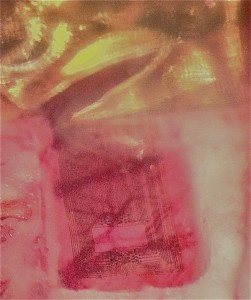
SBPMat newsletter: – In your opinion, what are your most significant contributions in the field of organic electronics/bioelectronics? Please explain them, very briefly, and share references from the resulting articles or books, or comment if these studies have produced patents, products, spin-off companies etc.
George Malliaras: – In the field of organic electronics it would be the co-development, together with Chris Ober at Cornell University, of orthogonal lithography. This is a set of processes that allows the microscale patterning of organic films using photolithography, the golden standard in microelectronics. Orthogonal lithography relies on the use of fluorinated photoresists that do not damage organic films. It allows the microfabrication of devices, including high resolution displays, using standard equipment that already exists in industry. There is a company (Orthogonal, Inc.,www.orthogonalinc.com) that has commercialized the photoresists and is pursuing commercialization of this technology. In bioelectronics, the work is too recent and I would have to wait for the benefit of hindsight. A trend that was emerging when I joined the field involved a transition from the use of organic coatings to the use of organic devices. The latter undoubtedly offer more capabilities to the interface with biology. My group is contributing to this trend by demonstrating that organic electrochemical transistors bring several benefits as transducers of biological phenomena, such as large amplification which enables high quality recordings of brain activity.
References:
SBPMat newsletter: – Which are, in your opinion, the main challenges for materials scientists and engineers about organic electronics interfacing with the brain?
George Malliaras: – To find the right collaborator who helps them formulate the right questions. I believe that embarking on an interdisciplinary field alone is a recipe for producing low impact work. The key to high impact work in this field is to formulate questions that are interesting to both neuroscientists and to us materials scientists and engineers. From our end, we need to be able to elaborate what are the advantages that organics offer and then figure out how to best employ them to address specific problems neuroscientists face. In my experience, it is often a combination of advantages (mixed conductivity, biocompatibility, “soft” mechanical properties) rather than a single one that gives the advantage to organics.
SBPMat newsletter: – If you wish, leave a message or an invitation to your plenary talk to the readers who will attend the XIV SBPMat Meeting.
George Malliaras: – I often quote a statement by Tadahiro Sekimoto, former president of Nippon Electric Corporation: “those who dominate materials, dominate technology”. It highlights the importance of materials research in our world and shows the dangers of moving to a “service” economy.
More
Prof. George Malliaras´ bio and abstract of his plenary lecture.
|
||||||||||||||||||||||||||||||||||||
The search for the materials that are most suitable for performing certain tasks maybe exists since the dawn of humanity. In this search, on the opposite end to the trial and error method, there is the combinatorial approach, which aims to increase the efficiency of the process of discovering or producing materials. This approach is based on the screening of large amounts of materials with compositions slightly different one another, using databases, rapid synthesis and characterization techniques, simulations, robots and other tools. The combinatorial approach has been applied to the pharmaceutical industry since the 1990s to identify new and useful compounds, and it also has its place in the field of Materials Science and Engineering.

During the XIV SBPMat Meeting, Professor Ichiro Takeuchi will give a plenary talk on the combinatorial approach to materials discovery – an issue that is part of his daily life. Takeuchi is a Professor of the Materials Science and Engineering Department at the University of Maryland, in the United States, since 1999. In this institution, he leads the Combinatorial Synthesis and Rapid Characterization Center and the Keck Lab for Combinatorial Nanosynthesis/ Multiscale Characterization. He is a Visiting Professor at the Tokyo University of Science since 2010. He is also member of the Executive Committee of the Forum on Industrial & Applied Physics from the American Physical Society (APS).
Takeuchi graduated with a Degree in Physics in 1987 at the California Institute of Technology (Caltech). For four years he worked in Japan at the microelectronics research laboratories of the NEC Corporation, to later return to the United States. In 1996, he earned his Ph.D. at the University of Maryland. Then, he went to the Lawrence Berkeley National Laboratory, where he stayed until 1999 as a postdoctoral researcher. In 2004, he was the chairman of the Gordon Conference on Combinatorial and High-throughput Materials Science. In 2009, he founded a company dedicated to the development of materials and systems for applications in the field of energy, the Maryland Energy and Sensor Technologies, LLC.
Ichiro Takeuchi was a Visiting Professor at universities in Japan and Germany. He has received awards and distinctions from the National Science Foundation (Career Award), the Office of Naval Research in the US (Young Investigator Program Award) and the University of Maryland, among other institutions. The scientist, whose H index is 40, according to Google Scholar, is the author of over 180 papers, with more than 5,900 citations, and a book on the combinatorial synthesis of materials.
What follows is a brief interview with this plenary speaker.
SBPMat newsletter: – Help us to visualize how the combinatorial research is performed. For instance, choose an example of a material created in your laboratories with this approach, and outline the “step-by-step”.
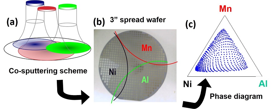
Ichiro Takeuchi: – We do thin film based combinatorial materials research. The goal is to carry out rapid screening of previously unexplored compositional landscape in order to discover new materials with enhanced physical properties. We make wafers or chips where there are large composition variations in deposited thin films. Sometimes the thin films are separated into different pads, and sometimes it is one continuous film with changing composition across the wafer. We want the variation to be as large and diverse as possible, so that we can map large compositional variation in a single experiment. We then take different characterization techniques to carry out rapid screening of various physical properties. For example, right now, we have a project to search for new permanent magnet materials. For this, we use techniques such as scanning SQUID or scanning magneto-optical Kerr effect measurements. These measurements can be used to map magnetic properties of all the compositions on a single wafer. These wafers and chips are called combinatorial libraries. We also do a lot of structural characterization. For this purpose, we often go to synchrotron beamlines. At such locations, because of the large beam flux, we are able to carry out x-ray diffraction of the entire wafer very quickly. Right now, we can scan 200-300 spots in 2 hours.
SBPMat newsletter: – In your opinion, what are your most significant contributions in the field of combinatorial materials science? Please explain them, very briefly, and share references from the resulting articles or books, or comment if these studies have produced patents, products, spin-off companies etc.
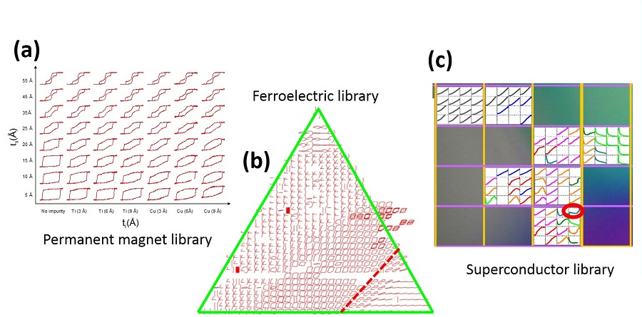
Ichiro Takeuchi: – Over the years, we have carried out combinatorial investigation on a variety of topics in the general field of functional materials. They include superconductors, shape memory alloys, magnetosrictive materials, ferroelectric and dielectric materials to name a few. In carrying out such experiments, we have had to develop and establish techniques to effectively implement the strategies. We have indeed discovered a number of new compounds. For instance, working together with theoretical colleagues, we have found shape memory alloys with long fatigue lives. I have patents on a number of low-loss dielectric materials as well as novel piezoelectric materials. Many groups are now doing follow-on work on a lead-free morphotropic phase boundary piezoelectric material we found a number of years ago. In addition to the materials that were discovered, we have established combinatorial strategies as a technique to rapidly delineate composition-structure-property relationships in different materials systems. We have recently published a comprehensive review article. It is: “Applications of high throughput (combinatorial) methodologies to electronic, magnetic, optical, and energy-related materials,” Journal of Applied Physiscs 113, 231101 (2013) by Martin L. Green, Ichiro Takeuchi, and Jason R. Hattrick-Simpers.
SBPMat newsletter: -If you wish, leave a message or an invitation to your plenary talk to the readers who will attend the XIV SBPMat Meeting.
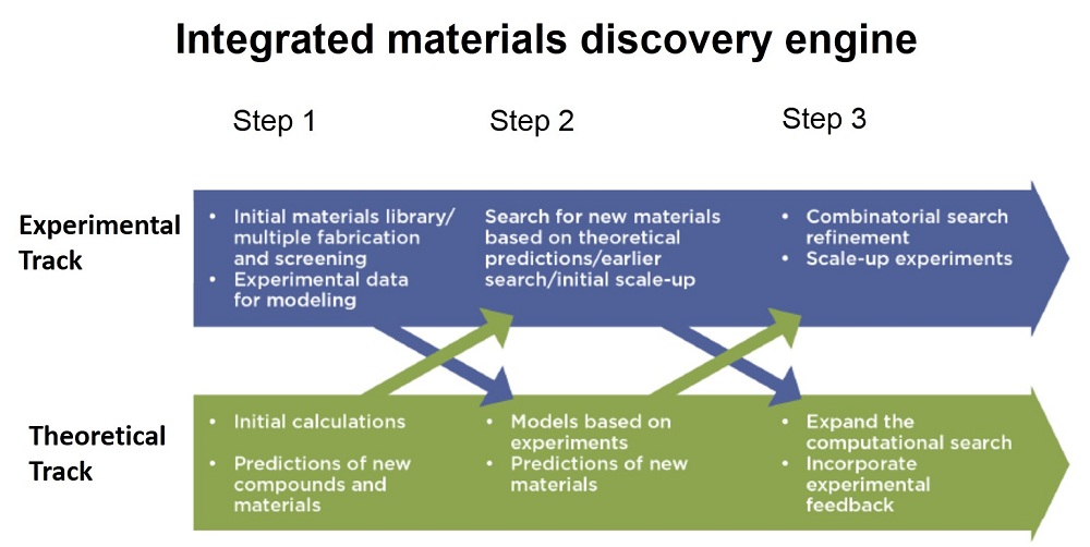
Ichiro Takeuchi: – The notion of search and discover is central to materials research. The combinatorial methodology is the natural counterpart to the concerted efforts in theoretical design of materials taking place around the world. By effectively coupling theory with high-throughput experimentation, we can really accelerate the rate at which new materials are discovered. I will present a mode of research we call “integrated materials engine” where theory and experiments are woven together and built on a flexible database and data management platform.
More:
|
||||||||||||||||||||||||||||||||||||
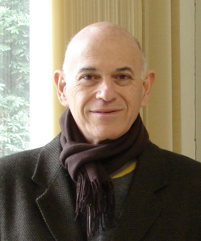 Israel Jacob Rabin Baumvol was born in Rio Grande do Sul, in the city of São Gabriel, in the last day of 1947. When he was a child, he moved to the city of Porto Alegre with his parents and siblings. When he was 19 years old, he entered the Federal University of Rio Grande do Sul (UFRGS) to study Physics. In the following years, in addition to participating in the political activity that occurred in the university against the existing military government, Baumvol dedicated a lot of effort to his studies, trying to reach the academic standard of the bachelor’s degree in Physics of the university. In 1971, he completed the graduation course – without honors, according to him. In the following year, he moved to the city of São Paulo to take a Master’s Degree in the University of São Paulo (USP), in Nuclear Physics and under the orientation of Professor Oscar Sala. In 1975, he returned to UFRGS to undertake his Doctorate, with orientation of Professor Fernando Zawislak, studying composites of perovskite structures. During the doctorate, he became a professor at UFRGS. In 1977, he defended his thesis. For the postdoctoral course, Baumvol chose an institution of industrial research in England, today known as Harwell campus. There, between 1979 and 1981, he worked with techniques of ionic implantation and its applications, mainly the plasma immersion ionic implantation (PIII), and he took part in research contracts with large companies. Due to his expertise in PIII, Baumvol entered the world of the materials for microelectronics, an area in which he made significant scientific contributions and obtained international reputation.
In the United States, Israel Baumvol was an invited researcher of the IBM research center from 1984 to 1988 and, from 1998 to 1999, of the Bell Laboratories, belonging to company Lucent. In France, between 1992 and 1996, he was a visiting professor at the Université Pierre et Marie Curie and at the Université Paris Diderot (Paris 7). In 1997, after coming first in a public entrance examination, he was nominated full professor at Paris 7, but he did not take over the position to stay in UFRGS. From 1995 to 1996, he was a guest professor of the Ruhr Universität, in Germany.
Baumvol was also coordinator of international events held outside Brazil. In 2000 and 2005, he was coordinator (chairman) of international symposia of Physical-Chemistry of silicon oxide and silicon – silicon dioxide interface, organized by the Electrochemical Society. In 2001, he coordinated the International Workshop on Device Technology of the Materials Research Society (MRS), held in Porto Alegre. In 2004, he was meeting chair of the MRS Spring Meeting & Exhibit, that occurs annually in San Francisco (United States).
In 2003, after retiring from his position of full professor of UFRGS, he led the creation of the Materials Science and Engineering Potgraduation Program of the University of Caxias of Sul (UCS), near 130 km far from Porto Alegre, and he was coordinator and researcher of the program until 2014.
From 2002 to 2003, Baumvol presided the Research Support Foundation of the State of Rio Grande do Sul (FAPERGS). More recently, between 2011 and 2013, he was vice-coordinator of the Materials Department in Capes (a federal agency for higher education improvement). Baumvol also coordinated big projects in the Materials segment, such as the first National Network of Research in Nanostructured Materials (2001-2005) and the National Institute of Surface Engineering (2009 to 2010).
Throughout his scientific career, Israel Baumvol has carried out research in subjects related to ionic implantation, thin layer physics and surface modification, in addition to materials for microelectronics.
Baumvol holds the highest productivity level scholarship in CNPq, the Brazilian federal science council. He has authored over 270 peer-reviewed articles, besides books and book chapters. His scientific production has approximately 3,000 citations. He acted as advisor in about 30 Master’s Degree and Doctorate dissertations.
In 2000, he was chosen Prominent Researcher by FAPERGS; in 2010, he was nominated Commander of the National Order of the Scientific Merit by the Presidency of the Brazilian Republic and in the following year, he was named Professor Emeritus by UFRGS. In May of this year, the “Professor Israel Baumvol Microscopy Center” was inaugurated in UCS.
Here is an interview with the scientist.
SBPMat newsletter: – Tell us what led you to become a scientist and to work in subjects of the Materials field.
Israel Baumvol: – It was the junction of three factors. The first one was the desire to use my knowledge one day to be able to contribute to the progress of the country and its citizens. This desire was developed through reading and great political participation during the graduation course. However, seeing as in Porto Alegre the tradition of basic research was very strong and there was nobody working in applied physics, I had a strict academic formation, that was very good for my future. The second factor was my post-doctorate, for which I chose an institution of industrial research, in England. I went there in 1979 to learn ionic implantation, because the institution was a pioneer in this method. There, I became acquainted with ionic implantation, specially its applications, such as reduction of the friction in metallic components (for example Ti-Al alloys) by means of implantation of species and heavy ionic composites, increase of the resistance to wear and corrosion of steel by nitriding, oxinitriding and nitrocarburizing using the method of ionic implantation by immersion in plasma (PIII). At that time, they were constructing there the first industrial-scale reactor of PIII, with a volume of approximately 30 m3, which was later spread throughout the world, including by companies that manufactured these reactors, such as Eaton and several others, including two companies in Brazil. This environment of applied physics fascinated me due to its possibilities. I participated in many research contracts, such as the one about bone prosthesis for a Japanese manufacturer, another about turbine blades for Rolls-Royce and another on cut blades for the future electric shavers project for Philips. These projects, in addition to fascinating me, had a component that for me was romantic: they were confidential projects. The third and last factor occurred by the end of my post-doctorate. I went to a congress in Germany, where I gave a 50-minute lecture, something very difficult nowadays, when the lectures only last about 20 minutes. When I finished speaking and answering questions, there was a coffee break. Dr. James F. Ziegler came up to me, introduced himself and gave me his business card, in which it was written “Research Director, Thomas J. Watson Research Center, IBM”. He invited me to go there because, during my lecture, he thought that the PIII method could solve a serious problem that IBM had with hard drives. Yet again, the siren song of a confidential project. I accepted the invitation and, for some years, during winter and summer vacations, three to four months per year, I went to IBM – Yorktown. There, I got in touch with something unusual for me, the silicon technology, which was just being born. That was yet another allure and my mind was made, Materials Science and Engineering.
SBPMat newsletter: – What are, in your own evaluation, your main contributions to Materials field?
Israel Baumvol: – I worked in many different subjects in my professional activity, some of them mentioned above. I will highlight three of them. The first one was my participation in the beginning of the PIII technology, which is nowadays widely used in the whole world, also in Brazil, where there are at least four services of PIII processes of steel components for the metal-mechanics industry. The second one is my contribution, throughout ten years of work, to explore and to reach the physical limits of silicon oxide as gate dielectric in the metal oxide semiconductor (MOS) technology. I formed a network of cooperation with academic laboratories in four different countries and with industrial laboratories, including IBM, Motorola, Texas Instruments, Bell-Lucent. We reached the physical limit, 1 nm. From there, the entire network started to work on a substitute for silicon oxide, which was the first change in the MOS technology, after forty years. There was a convergence for hafnium oxide and, eventually, certain hafnium-based double oxides. This material stood out, allowing an increase of processing speed and today it is used as gate oxide in advanced processors. It allowed the continuity of the Moore Law, which was threatened. This research segment led to the formation of a golden generation of PhDs, all around gate oxide, which is a crucial subject for the micro and nanoelectronics. Many of them are acting professionally in industrial companies, in technology of silicon and in other activities. Finally, I highlight the creation of a research environment in Materials Science and Engineering and of a post-graduate program in this segment. I started this activity with only one element: Caxias do Sul and its environs possess a large number of industrial companies, small, average and large companies needing research and human resources qualification. Only this, nothing more. Then, from nothing, I gathered some young high-qualified doctors and built the desired research environment, with many excellent laboratories and a very respectable post-graduation program. The impact on the industrial context of the region is notable and very recognized.
Bulletin of SBPMat: – Leave a message for our readers who are initiating their careers of scientists.
Israel Baumvol: – Follow your heart and not convenience. Take advantage of the doctorate, because this is the best time of the career: creative research and free from administrative responsibilities. Do not hesitate in showing your ideas. New ideas are not necessarily bad ideas. Use your post-doctorate to get in touch with the new and the unknown. Do not look for a place that works with the same subject of your doctorate research. Do not hesitate in changing the field, this is very stimulant and constitutes an important factor of individual progress. I pity the professionals who continue working in the subject of their doctorate theses, ten or twenty years after the conclusion. Applied research can very be good research. Get rid of preconceptions, it does not matter if the research is fundamental, or applied or directly industrial. What counts is quality. The only difference is between good quality research or bad quality research.