 In the late 1950s, solar cells where used for the first time in artificial satellites. Today, these devices that produce electricity from sunlight thanks to the property of some materials to release electrons when absorbing photons, are part of the energy matrix of many countries, besides being used in all sort of spacecraft. Several technologies based on different materials have been developed to make this sustainable production of electricity. However, research in the area is still very intense. While silicon solar cells dominate the current market, other technologies can compete with silicon in economic and environmental terms.
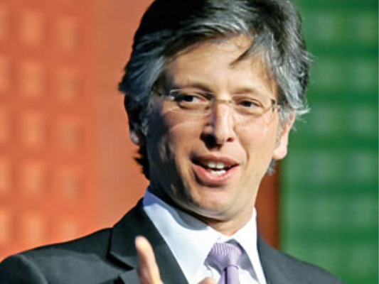
In a plenary lecture at the XV Brazil-MRS Meeting, Anders Hagfeldt, Professor at École Polytechnique Fédérale de Lausanne (EPFL), Switzerland, will talk about recent advances on some solar cells technologies that are alternative to the silicon one, in particular those based on perovskite materials and those based on dye sensitized thin films (known as dye-sensitized solar cells, DSSCs). Hagfeldt has been performing research on both types of solar cells, and succeeded in improving their efficiency using different methods and new materials.
Hagfeldt obtained his diploma of Master of Science in Physics and Chemistry from Uppsala University (Sweden) in 1989 and started his doctoral studies in the same university. In 1993, he concluded his PhD with a thesis on microporous and polycrystalline semiconductor electrodes. Then he went to EPFL, in Switzerland, where he was a postdoctoral fellow with Prof. Michael Grätzel, the inventor of the DSSCs.
In 1994 he went back to his alma mater (Uppsala), first as a junior researcher and then as a Professor in Chemical Physics and Physical Chemistry. He was a Visiting Professor at the Royal Institute of Technology (Sweden) from 2005 to 2010, and at the Institute of Materials Research and Engineering (Singapore) from 2008 to 2010. In 2009, he co-founded Dyenamo, a company dedicated to materials and equipment for solar energy applications.
Since 2014, Hagfeldt is a Full Professor of Physical Chemistry at EPFL, where he heads the Laboratory of Photomolecular Science. Besides, he is a Visiting Professor at Uppsala University and Nanyang Technological University (Singapore). He is a member of the European Academy of Sciences, Royal Swedish Academy of Sciences, Royal Society of Sciences in Uppsala, and the Royal Swedish Academy of Engineering Sciences.
Anders Hagfeldt´s was ranked in various international lists of highly cited researchers, such as the Thomson Reuter’s list of the top 1% most cited in Chemistry (2014-2016) and the top-100 material scientists of the past decade by Times Higher Education (2011). In fact, Hagfeldt authored above 400 papers with more than 47.000 citations and has an h-index of 103, according to Google Scholar. Moreover, he is the author of 9 patent applications.
Here follows a short interview with Professor Anders Hagfeldt.
SBPMat newsletter: – Could you state, very briefly, which are the main advantages and disadvantages of the different solar cells technologies, in terms of efficiency, cost and other relevant criteria?
Anders Hagfeldt: – When it comes to different technologies, the very dominant technology has been for long time based on silicon material, the “silicon solar cells”. In terms of market share, I think that around 90% of all solar cells stored in the world are silicon solar cells. They are mainly produced in China. Silicon has always had the advantage of being efficient and very stable, robust, durable. So, you can get, for example, guarantees of lifetime of over 20 years. If you go few years back, it was always said that silicon solar cells were too expensive and that they wouldn´t never be competitive with other energy technologies, such as fossil fuels and so on. However, five years ago, the production volume has increased a lot and the prize has became unexpectedly lower. Actually, silicon solar cells can be considered quite cheap today. Therefore, silicon solar cells are very good. They have good performance at low cost and match the price in kilowatt-hour of other energy technologies such as burning liquid hydrocarbons, for example.
The next class of technology is called “thin-film solar cells”, and it comprises two different materials. One is known as CIGS, that comes from copper indium gallium selenide, which is the material that absorbs sunlight. The other material is cadmium telluride (CdTe). The latter solar cells are manufactured in a big company in the United States called First Solar. Both of these technologies have the promise to be cheaper than silicon technology. They are almost as efficient as silicon: 10% to 15% less efficient. Both materials are disposed in very thin films, so the materials cost is low and, probably, they can be produced cheaper than silicon solar cells. Therefore, the key thing for thin films to be able to compete with silicon is to be a little bit higher in efficiency and scaling up the production.
These are the three main commercially available technologies today. If we go to research activities, the most “hype” at the moment is the perovskite solar cell. It had its breakthrough only four years ago, and during these few four years, it has reached similar efficiencies as thin-film solar cells. That has been the fastest development in solar cells. Perovskite solar cells will probably be cheaper than thin-film solar cells, but they are still in a research stage. The main question mark of perovskite solar cells has been on stability. In that point, we have made some breakthroughs. Two papers of us have been accepted by the Science journal reporting very promising stability data for perovskite solar cells. That is something I will report on the Brazil-MRS Meeting as a key or latest result of perovskite technology. It is very exciting, perovskite solar cells are not fundamentally unstable, they show promising stability. However, there is a lot of work to be done in terms of scaling up and further stability testing and development.
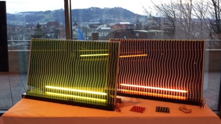
The other technology I will talk about is dye-sensitized solar cells (DSSC), which is also in research or demonstration level. They are lower in efficiency, so, what we look for in that technology today is niche applications. These cells are based on dyes, which means that you can make them in different colors, and use them in windows, buildings and so on. At the moment, DSSC cannot compete with silicon for large scale, but there is interest for buildings, consumer electronics, rechargeable batteries, keyboards and so on.
SBPMat newsletter: – In your opinion, which are the main next challenges in the field of solar cell research and development?
Anders Hagfeldt: – I can divide this answer in two parts.
Firstly, there is still room and it is still important to make solar cells more efficient to lower the cost of the kilowatt-hour produced. There is a kind of dream target I see. This is not really in my expertise, but I listen to more industrial people talking about U.S. dollar cents per kilowatt-hour (how much costs for solar cell to produce a kilowatt-hour). And it seems that now this cost can go down to 4 cents per kilowatt-hour, which is very good, but it could be cheaper. People say that it can go down to 2 cents per kilowatt-hour. The best thing you can do today to lower the cost per kilowatt-hour of solar cells is to try to increase their efficiency. That is where you see the potential of the perovskite solar cells, because they have had such a fast development and they are already at the same level of established technologies. It seems promising that these perovskite solar cells can show even higher efficiencies than the silicon ones. That is a big challenge but I think it is not impossible.
The second thing is that solar cells is intermittent, that means that they only produce electricity when there is sunshine. During nights and evenings, this is a problem. I come from Sweden that is a country where more electricity is needed when there is less sunshine. That means that you also have to find the storage for electricity.
These key challenges are not for solar cell itself, but for the whole picture of solar energy.
More and more solar cells are being used to produce electricity, but that creates problems to the utility grid, because there can be too much electricity when it is sunny day and too little when it is not sunshine. Therefore, we need to work on storage. I think that for small scale, batteries are interesting, but for larger scale, we need to find how to produce fuel from sunlight or from the electricity produced. And that can be hydrogen, that is something people look into a lot, but also for example methanol.
SBPMat newsletter: – Leave an invitation for our readers to attend your plenary lecture “The Versatility of Mesoscopic Solar Cells”.
Anders Hagfeldt: – I am very happy to go to Brazil. I have been around before, some years back, but I am very excited to meet new people to discuss our research at the meeting. Everyone will be very welcome and I will be very happy to discuss all kind of ideas and questions.
——————————–
Link to the abstract of Anders Hagfeldt´s plenary lecture at the XV Brazil-MRS Meeting: http://sbpmat.org.br/15encontro/speakers/abstracts/9.pdf