|
||||||||||||||||||||||||||||||||
|
||||||||||||||||||||||||||||||||
 Computational methods make a difference when the challenge is to develop a new material for a given technology or to adjust material properties to fit a specific application.
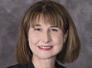
In the end of September, the computational materials scientist Susan Sinnott will talk about this topic of her expertise in a plenary lecture at the XV Brazil-MRS Meeting. Sinnott is Professor and Department Head of Materials Science and Engineering at Pennsylvania State University (USA). She is also the editor-in-chief of “Computational Materials Science” (Elsevier).
Susan Sinnott received her B.S. degree in Chemistry (with honors) from the University of Texas in 1987 and her doctoral degree in Physical Chemistry from Iowa State University in 1993. Then she worked as a postdoctoral associate at the U.S. Naval Research Laboratory until 1995. After that, she became a faculty member of the University of Kentucky. In 2000, she began her tenure at the University of Florida (UF). In 2012, she was named the Alumni Professor of Materials Science and director of the Cyberinfrastructure for Atomistic Materials Science at UF. In 2013, she was president of the American Vacuum Society (AVS). In 2015, she joined the Pennsylvania State University (Penn State).
Susan Sinnott is the author of more than 210 refereed journal papers and 8 book chapters. She has over 10,000 citations and an h-index of 46, according to Google Scholar.
She is a Fellow of the Materials Research Society, American Physical Society, American Ceramic Society, American Vacuum Society, and American Association for the Advancement of Science.
In the XV Brazil-MRS Meeting, Susan Sinnott will not only deliver the plenary lecture “Role of Atomic-Scale Modeling in Materials Design and Discovery”, but also take part in the roundtable “Meet the editors” to discuss scientific publication issues. Besides her position as editor-in-chief of “Computational Materials Science”, this scientist serves as associate editor, principle editor and divisional associated editor for other journals.
Here follows a short interview with the scientist.
SBPMat newsletter: – In your opinion, what are your most significant contributions to the field of materials modeling? Explain them very briefly and, if possible, share references of resulting publications or patents, products etc.
Susan Sinnott: – My research program uses computational atomistic methods to design and investigate materials. This area has seen tremendous growth in the last two decades because of a combination of factors, including the increasing availability and low cost of fast computers, the refinement of atomistic methods, the shrinking of device dimensions, and the improved ability of experimentalists to study materials at the nanometer scale. It approaches well-established continuum level modeling (such as finite element analysis) and fluid dynamics at high length scales (100s-1000s nanometers), and overlaps with traditional physics and chemistry at small length scales (1-10 nanometers).
A major contribution from my research group is the development of inventive methods to enable the modeling of new material systems at the atomic level. In particular, my collaborators and I developed a new empirical, reactive potential for molecular dynamics simulations that allows for the modeling of heterogeneous material systems at the atomic scale, something that has traditionally only been possible with computationally intensive first principles methods such as density functional theory. This method has allowed us to investigate such otherwise intractable problems as Cu thin film growth on ZnO surfaces, and model the catalytic activity of metal clusters on oxide surfaces. These potentials have been incorporated into an open-source massively parallel molecular dynamics software developed at Sandia National Laboratory to make them available to the modeling community.
Some relevant publications are:
SBPMat newsletter: – In the abstract of your plenary lecture, you mention the concept of “materials by design”. Could you explain this idea in a few words? Today, is “materials by design” a fact or a promise?
Susan Sinnott: – The ability to design a material with desired properties a priori using computational methods has been a promise of the field of computational materials science for many years. This promise relies on designing materials that do not currently exist or with properties that are desired from compositions that are largely unknown. The day that we can input the properties desired for a given part or device into a computer and have it predict the composition and microstructure or morphology needed to produce those properties has not yet arrived but remains the ultimate goal of “materials by design” initiatives. Currently, the integration of computational and experimental approaches is more complete than ever before. This enables computational materials science methods to make predictions that can be subsequently validated, and for experimental observations to be explained. Advances depend on continued improvements in the accuracy and predictability of computational methods along with continuing improvements in the linkages of the computational results to data from experimental characterization and production methods. An integral component to the new paradigm for materials design and discovery is the production and integration of datasets from calculations, simulations, experiments, or a combination of all of these. Therefore the seamless integration of database mining and materials informatics methods with conventional experimental and computational materials science methods is required. Lastly, the materials community must reach a critical comfort level and associated understanding of the strengths and limitations of coupling these methods so that such comparisons can be made on a routine basis.
A relevant paper that discusses these ideas in more detail is:
“Material design and discovery with computational materials science”, S.B. Sinnott, Journal of Vacuum Science and Technology A 31, 050812 (2013)
SBPMat newsletter: – If you desire, leave an invitation for our readers to go to your plenary lecture at the XV Brazil-MRS Meeting.
Susan Sinnott: – I invite you to find out more at my plenary lecture at the XV Brazil-MRS Meeting.
Link to the abstract of Susan Sinnott´s plenary lecture at the XV Brazil-MRS Meeting: http://sbpmat.org.br/15encontro/speakers/abstracts/10.pdf
[Paper: Topologically Protected Metallic States Induced by a One-Dimensional Extended Defect in the Bulk of a 2D Topological Insulator. Erika N. Lima, Tome M. Schmidt, and Ricardo W. Nunes. Nano Lett., 2016, 16 (7), pp 4025–4031. DOI: 10.1021/acs.nanolett.6b00521]
Isolating nanoribbons with conducting regions
A research carried out in Brazil made an important contribution to the study of topological insulators, a class of materials that was theoretically predicted in 2005 and experimentally confirmed in 2007. The study was reported in an article recently published in Nano Letters (impact factor: 13.779).
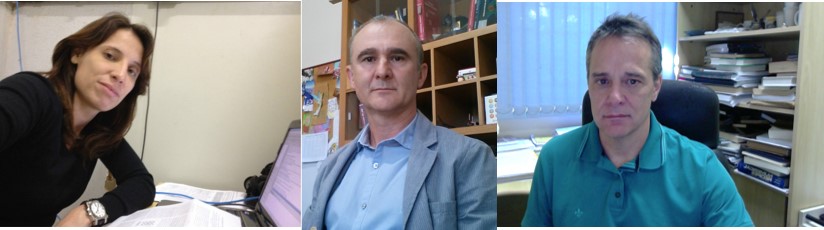
A unique property of Topological insulators is that they behave as insulators on the inside and as conductors on its surface or edge. According to Ricardo Wagner Nunes, professor at the Federal University of Minas Gerais (UFMG) and corresponding author of the article, “non-topological insulators may also have conductive surfaces, but in the case of topological insulators, conduction of charge and spin on the surface is robust, as it is “protected” by time reversal symmetry”.
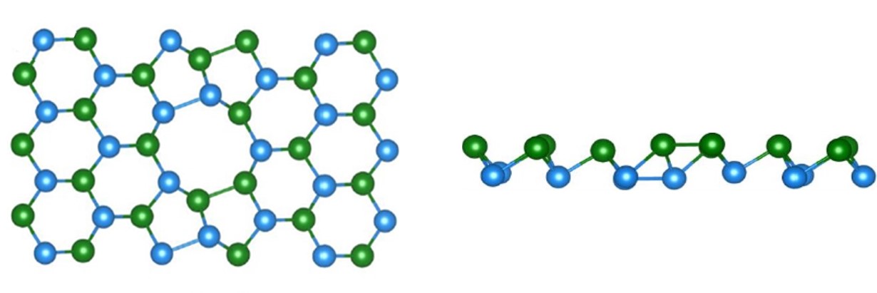
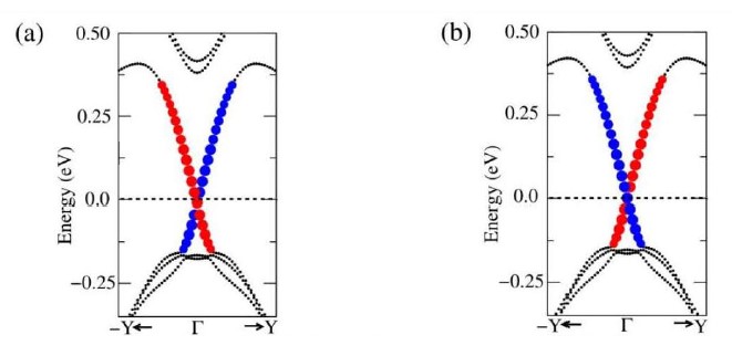
In the article in Nano Letters, Professor Nunes and colleagues, Erika Lima, of the Federal University of Mato Grosso (UFMT) – Rondonópolis campus, and Tome Schmidt, of the Federal University of Uberlândia (UFU), reported their work on a two-dimensional topological insulator, a bismuth nanoribbon of only two layers of bismuth atoms (one-atom thick), superimposed and bonded. Using computational methods, the scientists showed that the interior of the bismuth nanoribbon, instead of being fully insulating, may have conductive states (also called metallic states) generated from a particular type of irregularity in the atomic structure of the material, known as 558 extended defect.
“In our work, we show that a linear defect within a two-dimensional topological insulator can generate one-dimensional electronic quantum states that conduct spin and charge within the material”, say the authors.
This conclusion was supported through calculations performed on supercomputers, simulating what would happen to the electrons in quantum states, in the material, in the presence of defects. “We used first-principles Density Functional Theory calculations”, specify the authors, who relate that the computer simulation of defects in bismuth nanostructures required approximately 400 hours of computer simulations on supercomputers in the Department of Physics – UFMG and at the National Center for High Performance Computing in São Paulo (Cenapad) – UNICAMP.
In the article, the authors also propose the existence of pentaoctite, a new two-dimensional topological insulator. This material, which has not been synthesized yet, is a bismuth bilayer with a crystal lattice formed by atoms arranged in pentagons and octagons. As stated by the authors, “In our calculations we show that this new “phase” of the two-dimensional bismuth has low formation energy, which opens the possibility to be synthesized in the laboratory”.
According to the authors, the work reported in Nano Letters raises several issues in the scope of fundamental research, such as the influence of magnetic and non-magnetic impurities on the spin and charge transport in the proposed topological states, and the connection between the network symmetries and nature of the topological edge states on pentaoctite. “From the point of view of applications, it would be interesting if our work could motivate experimental studies of two-dimensional topological insulators based on bismuth and other materials, enabling theoretical and experimental collaboration on this issue”, comment the authors, leaving an open invitation to experimental research groups.
The origin of this research work
“The work originated by combining my interest in extended topological defects in two-dimensional and three-dimensional materials, with the experience of Professor Tome Mauro Schmidt (UFU) and Erika Lima, his doctoral student in the subject of topological insulators”, states Nunes.
In 2012, Nunes and collaborators published an article in Nano Letters on magnetic states (non topological) generated by linear extended defects in a monolayer of graphene. Later, in a conversation with Schmidt, a collaboration was decided in order to investigate if an extended defect with the same morphology would lead to the formation of topological states in a bidimensional topological insulator made of bismuth.
In her post-doctorate in the group of Professor Nunes, in 2015, Erika Lima performed all computer calculations. The three researchers, who are the authors of the article, interpreted the results and wrote the paper.
The research that led to the article received funding from Brazilian agencies CAPES, CNPq, FAPEMIG and from the National Institute of Science and Technology on Carbon Nanomaterials.
Professor Victor Carlos Pandolfelli, of the Department of Materials Engineering, Federal University of São Carlos (DEMa-UFSCar) was chosen to serve as one of the editors-in-chief of the journal Ceramics International. The international journal with 41 years of history is published by Elsevier. It currently has an acceptance rate of 25% of the articles submitted.
Pandolfelli completed his doctorate in Leeds (UK) in 1989 and in 1996 and 1997 he completed his postdoctoral studies at the École Polytechnique in Montreal (Canada). He is full professor at DEMa-UFSCar, member of the Brazilian Academy of Sciences, full member of the World Academy of Ceramics, a fellow of the American Ceramic Society, full member of the Brazilian National Academy of Engineering and guest professor at Wuhan University of Science and Technology (China). He is a member of the board of the World Academy of Ceramics (2014-2018), member of the International Technical Board of Morgan International (England) and Latin American coordinator of the FIRE (Federation for International Refractories Research and Education), which involves 10 universities in different countries and 17 leading companies in the refractory area. He is the author of 480 articles published in scientific journals and two books. He has received 12 international awards.
The Laboratory of Bioelectrochemistry and Interfaces at São Paulo University (USP), campus at São Carlos, São Paulo state, Brazil, invites applications for a postdoctoral research fellowship in bioelectrochemistry under supervision of Professor Frank Crespilho and funded by Foundation for Research Support of the State of São Paulo (FAPESP) contract. The successful candidate will conduct research on the molecular interaction between biomolecules and nanostructures, including:
Fellowship for postdoctoral researchers allows you to carry out a long-term research project (12-24 months), starting at 10/2016.
Applicants must have a Ph.D. in chemistry, chemical engineering, electrochemical engineering, or a related field. Experience in enzymes immobilization and basic electrochemistry is required. Experience with UV-Vis spectroscopy, and FTIR spectroscopy, is preferred. The successful candidate must have excellent communication skills and excel in a highly collaborative research environment. In addition to the timely publication of research results in peer-reviewed journals, the responsibilities of the postdoc include drafting progress reports. Interested individuals should send a (i)cover letter, (II) CV and list of publications, and have (III) two letters of recommendation sent to bioelectrochemistry@iqsc.usp.br. The deadline for application is 09/11/2016.
Vaga para professor adjunto 40h – DE no Programa de Engenharia de Nanotecnologia da COPPE.
Mais informações e inscrições: http://concursos.pr4.ufrj.br/index.php/component/content/article/37-concursos/concursos-em-andamento/edital-215-de-29-de-junho-de-2016/333-edital-215-de-29-de-junho-de-2016
The Brazilian Materials Research Society (SBPMat) is pleased to announce that the XVI Brazil-MRS Meeting will be held in the city of Gramado (State of Rio Grande do Sul, Brazil) from 24 to 28 10 to 14 of September, 2017.
Save the date!