Tag: ciência de materiais
SBPMat newsletter. English edition. Year 1, issue 9 – special: XIII SBPMat Meeting.
|
||||||||||||||||||||||||||||||||
Interviews with plenary lecturers of the XIII SBPMat Meeting: Robert Chang (Northwestern University, USA).
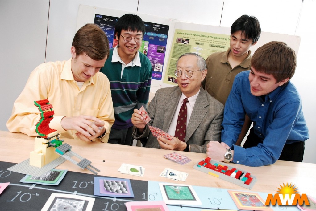
Robert Chang is a Professor of Materials Science and Engineering at the first materials science academic department in the world, created more than 50 years ago at Northwestern University, where he is also director of the Materials Research Institute.
He holds a Bachelor of Science in Physics from Massachusetts Institute of Technology (MIT) and a Ph.D in Plasma Physics from Princeton University. He spent 15 years performing basic research at Bell Labs (Murray Hill). During the past 28 years at Northwestern University, he has directed several National Science Foundation (NSF) centers and programs in materials research and education.
Prof. Chang was the president of the Materials Research Society (MRS) in 1989. He is the General Secretary and Founding President of the International Union of Materials Research Societies (IUMRS). He has received many distinctions for his work, such as the Woody Award from MRS in 1987, the Siu Lien Ling Wong Fellow from the Chinese University of Hong Kong in 1999, and the NSF Director’s Distinguished Teaching Scholar Award in 2005. He is fellow of the American Vacuum Society and MRS, and honorary member of Materials Research Societies of India, Japan and Korea.
He is (co)author of 400 peer reviewed journal articles, with near 13,000 citations, and h-index of 56.
Read our interview with the plenary speaker.
SBPMat newsletter: – Under your viewpoint, which are your main contributions in the field of Materials Science and Engineering?
Robert Chang: 1. Plasma processing of semiconducting materials;
2. Carbon based materials, such as diamond, fullerene, and carbon nanotubes, and their related devices;
3. 3rd generation solar cells;
4. Infrared plasmonics and sensors;
5. Thin film oxides for electronic and photonic devices.
Top publications below.
H. Cao, Y. G. Zhao, S. T. Ho, E. W. Seelig, Q. H. Wang, and R. P. H. Chang. Random Laser Action in Semiconductor Powder. Phys. Rev. Lett. 82, 2278 (1999); DOI:http://dx.doi.org/10.1103/
Michael D. Irwin, D. Bruce Buchholz, Alexander W. Hains, Robert P. H. Chang, and Tobin J. Marks.p-Type semiconducting nickel oxide as an efficiency-enhancing anode interfacial layer in polymer bulk-heterojunction solar cells. PNAS, vol. 105 no. 8, 2783–2787 (2008); doi: 10.1073/pnas.0711990105.
Q. H. Wang, A. A. Setlur, J. M. Lauerhaas, J. Y. Dai, E. W. Seelig and R. P. H. Chang. A nanotube-based field-emission flat panel display. Appl. Phys. Lett. 72, 2912 (1998);http://dx.doi.org/10.
Quanchang Li, Vageesh Kumar, Yan Li, Haitao Zhang, Tobin J. Marks, and Robert P. H. Chang. Fabrication of ZnO Nanorods and Nanotubes in Aqueous Solutions. Chem. Mater., 2005, 17 (5), pp 1001–1006. DOI: 10.1021/cm048144q.
SBPMat newsletter: – And what about your main contributions to science education, especially in Materials Science?
Robert Chang: – Over the past 20 years, I have led the development of the Materials World Modules program to teach pre-college students about Materials and Nanotechnology: materialsworldmodules.org; nclt.us; gsasprogram.org; imisee.net.
SBPMat newsletter: – Please give us a short teaser about your plenary talk at SBPMat meeting. What do you intend to broach?
Robert Chang: – Mobilizing world-citizens to solve global problems together!
SBPMat newsletter: – Feel free to leave other comments to our readers from the Materials research community, if you want so.
Robert Chang: – Materials and nanotechnology research and education are the driving force of all future technologies, including energy, environment, health, and security.
(Português) Processo seletivo para bolsas de pós-doutorado CAPES/PNPD no Programa de Pós-Graduação em Física da UFSC-Florianópolis.
SBPMat newsletter. English edition. Year 1, issue 8.
|
||||||||||||||||||||||||||||||||||||||||
Featured paper: Accurate engineering in spin valves manufacturing.
The scientific paper by members of the Brazilian community on Materials research featured this month is:
T. E. P. Bueno, D. E. Parreiras, G. F. M. Gomes, S. Michea, R. L. Rodríguez-Suárez, M. S. Araújo Filho, W. A. A. Macedo, K. Krambrock and R. Paniago.Noncollinear ferromagnetic easy axes in Py/Ru/FeCo/IrMn spin valves induced by oblique deposition. Appl. Phys. Lett. 104, 242404 (2014). DOI: 10.1063/1.4883886.
Accurate engineering in spin valves manufacturing
The production and characterization of spin valves is the theme of a collaborative work between Brazil and Chile, whose results were published recently in the prestigious journal Applied Physics Letters (APL).
Spin valves are devices consisting of three or more layers of nanometric thickness composing a sandwich of magnetic and non-magnetic materials. Sensors consisting of such structures fulfill a fundamental role in reading the information written on the hard disc drives, among other applications.
The operation of spin valves is based on an effect called “giant magnetoresistance”, which was the reason behind the Nobel Prize in Physics in 2007. The giant magnetoresistance of spin valve consists of a large change in the electrical resistance in response to the action of a magnetic field. This resistance depends on the relative orientation among the magnetization of the magnetic material layers.
The magnetization of a magnetic material is determined by the orientation of the spins of its electrons. Electrons have two intrinsic features: electric charge and magnetic moment, the latter known as spin. Explore the degree of freedom of the electron spin in addition to its charge led to the emergence of a new field of research called spintronics.
Then, on giant magnetoresistance of spin valves, when the layers of magnetic material have the same direction of magnetization, the device reduces its electrical resistance and becomes a better conductor of electricity. When the magnetic layers acquire opposite directions of magnetization, a significant increase of electrical resistance occurs.
For better understand this effect and, later, the results presented in the article of APL, it is important to remember that the magnetization is a vector physical quantity and that, therefore, besides having an intensity, it has a direction (parallel, perpendicular) and an orientation (indicated by the arrowhead representing the vector). Usually, metallic multilayers composed of magnetic materials separated by a non-magnetic layer, as spin valves, have the magnetization of ferromagnetic layers coupled, says Thiago Bueno, first author of the APL article and PhD student in Physics at the Brazilian Federal University of Minas Gerais (UFMG), supervised by professor Roberto Magalhães Padilla. This coupling can result in parallel magnetization (called “collinear”) with same or opposite orientations, and also in non-collinear magnetization.
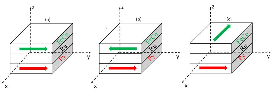
However, to magnetize the magnetic layers of the spin valve does not occur homogeneously in all directions; they feature the so-called magnetic anisotropy. “The magnetic anisotropy is an important magnetic property, because it establishes an easy direction of magnetization,” says Thiago Bueno. “This property is determined by a number of factors, including the types of materials, the thickness of layers, and the details of the method of sample manufacturing”.
On the work that originated the APL article, the team of scientists has made some adjustments to the method of spin valves manufacturing, obtaining interesting results on the properties of these devices.
Controlling the direction of magnetization
“This work was only possible due to the great collaboration between the parties along the preparation of samples of excellent quality, accurate experimental measures, interpretation of the data, until the publication of the results,” says Thiago Bueno.
Initially, at the Brazilian Center for Development of Nuclear Technology (CDTN in Portuguese) the team has made thin films composed of multi-layers with thickness of a few tens of nanometers. The films were obtained through the technique known as magnetron sputtering, in which argon ions are accelerated against the targets that contain the materials to be deposited, ripping off its atoms. With the aid of magnetrons, these atoms are deposited on a substrate, forming the layers of films. “Through this technique it is possible to obtain films with well-determined chemical composition, thickness and structural morphology,” says Thiago Bueno.
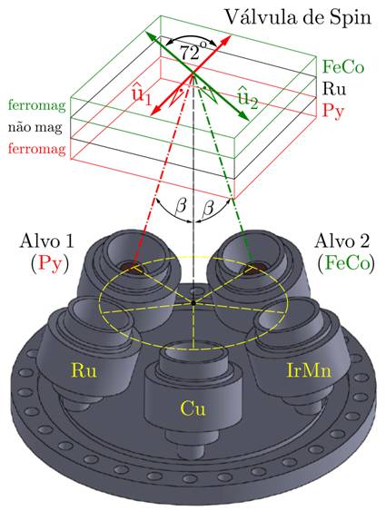
In this study, the scientists set up an oblique deposition scheme by putting the magnetrons making an angle of 72o between them and inclined towards the sample. Using the oblique deposition scheme, scientists made spin valves with ferromagnetic layers up to 10nm-thickness, composed of metallic alloys (Py and FeCo), and separated by a non-magnetic layer of ruthenium (Ru) of thickness between 1nm and 3.5nm. The devices were characterized in the Physics Department at UFMG using ferromagnetic resonance (FMR), an extremely sensitive technique that provides relevant information on the magnetization of materials.
After the interpretation of experimental results, which involved researchers from the Pontifical Catholic University of Chile, the scientists concluded that the oblique deposition induced non-parallel magnetization directions (non-collinear) on ferromagnetic layers of manufactured spin valves. “The angle between the easy axes, approximately equal to the angle between the magnetrons, was determined by the manufacturing geometry”, reinforces the author, Bueno. “One of the main contributions of our work is the demonstration that it is possible to manufacture spin valves where the axes of easy magnetization of ferromagnetic layers (Py and FeCo) are non-collinear,” he sums up.
According to the doctoral student, at the beginning of the work the authors already knew the oblique deposition effects in ferromagnetic/anti-ferromagnetic bilayers. With this study, the team took a step further and has investigated these effects in a more complex structure, the spin valve.
“We believe that our work will compel other researchers into manufacturing these devices, seeking new magnetic configurations between layers of the spin valve “, says Bueno.
Interviews with plenary lecturers of the XIII SBPMat Meeting: Karl Leo (TU Dresden, Germany).
The German physicst Karl Leo studied physics at the Albert Ludwigs University of Freiburg (Gemany) and obtained the “Diplomphysiker” degree with a thesis on solar cells at the Fraunhofer Institute for Solar Energy Systems (Germany). In 1988, he obtained the PhD degree from the University of Stuttgart for a doctoral thesis performed at the Max Planck Institute for Solid State Research in Stuttgart. From 1989 to 1991, he was a postdoc at AT&T Bell Laboratories (United States). In 1991 he joined the RWTH Aachen University (Germany) as an assistant professor and obtained the Habilitation degree. In 1993 he joined the Dresden University of Technology (Germany) as a professor of optoelectronics. Since 2001 until 2013, he has been also with the Fraunhofer Institute for Photonic Microsystems, being head of department and then director.
He won some of the most prestigious German awards in science, technology and innovation, such as the Leibniz award (2002) and the German Future Prize (2011).
He is the author of more than 550 refereed publications, with more than 23.000 citations, having an H index = 73 (Google Scholar). He is (co-)inventor of approximately 50 patent families.
Since 1999 he has co-founded 8 spin-off companies, such as Heliatek and Novaled, which have employed more than 250 people and raised more than 60M€.

Read our interview with the lecturer.
SBPMat newsletter: – Under your viewpoint, which are your main contributions in the field of Materials Science and Engineering? Please think about papers, patents, spin-off companies, products etc.
Karl Leo: – I spent most of the last decades improving organic semiconductors and developing new device concepts for organic semiconductor devices. One example is the development of controlled electrical doping, which allowed much higher electrical conductivities. As a result, we could e.g. realize white organic light emitting diodes which are more efficient than fluorescent tubes. As device principle, we e.g. developed novel vertical transistors which can drive very high currents so that they can be used to drive OLED displays.
SBPMat newsletter: – Please give us a short teaser about your plenary talk at the XIII SBPMat meeting. What do you intend to broach?
Karl Leo: – I will talk about highly efficient organic devices, touching both organic LED and organic solar cells. I will describe the challenges in materials research and the importance of new device concepts.
SBPMat newsletter: – Could you choose some of your main publications (about 3 or 4) on the topics of your plenary lecture to share them with our public?
Karl Leo: –
1. Doped Organic Transistors: Inversion and Depletion Regime. Lüssem, B., Tietze, M.L., Kleemann, H., Hoßbach, C., Bartha, J.W., Zakhidov, A. and Leo, K. , Nature Comm. 4, 2775 (2013).
2. Phase-locked coherent modes in a patterned metal-organic microcavity. Brückner, R. Zakhidov, A., Scholz, R., Sudzius, S., Hintschich, S.I., Fröb, H., Lyssenko, V.G. and Leo, K., Nature Photonics 6, 322–326 (2012).
3. White organic light-emitting diodes with fluorescent tube efficiency. Reineke, S.; Lindner, F.; Schwartz, G. et al., Nature 459, 234 (2009).
SBPMat newsletter: – Feel free to leave other comments to our readers from the Materials research community.
Karl Leo: – The field of materials research is as exciting as ever, and in the field of organic semiconductors, we are still in the beginning, maybe where silicon was in 1970…
SBPMat newsletter. English edition. Year 1, issue 7.
|
||||||||||||||||||||||||||||||||
Made in Brazil: incorporating silver nanostructures into oral hygiene products eliminates 99% of bacteria and fungi.
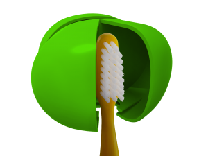 A research on the incorporation of silver with antibacterial properties on surfaces, conducted by the Center for the Development of Functional Materials (CDMF in Portuguese), one of the Research, Innovation and Dissemination Centers of the São Paulo Research Foundation (FAPESP) is being applied to toothbrushes.
OralGift, a company with 12 years of experience in the oral hygiene business, in association with CDMF and NANOX Tecnologia, released a new line of products coated with the NanoxClean technology. Produced with silver nanostructures incorporated into the raw materials, the surface of the product is protected against microorganisms and bacteria.
The researchers responsible for this work explain that damp environments, mainly bathrooms, display a large amount of bacteria and fungi. When toothbrushes are left exposed, there is a high possibility of contamination.
The technology incorporating silver nanostructures eliminates 99% of the bacteria and fungi accumulated on toothbrush and the cases used to keep them, as well as tongue cleaners.
The CDMF Director, Professor Eldon Longo, clarifies the importance of the association between the research developed at the university and the industrial-scale innovation made in companies: “Nanox is a first world company in innovation, with high technology. It develops products based on nanotechnology, mainly to healthcare. This innovation, released on the market, is another example of creativity in transforming knowledge into wealth for the country”.
About CDMF
The Center for the Development of Functional Materials (CDMF) is one of the Research, Innovation and Dissemination Centers (CEPID in Portuguese) supported by FAPESP (São Paulo Research Foundation), and the National Institute of Science and Technology of Materials in Nanotechnology, and counts with the collaboration of São Paulo State University (Unesp), Federal University of São Carlos (UFSCar), University of São Paulo, (USP) and the Nuclear and Energy Research Institute (Ipen).
Facebook profile: https://www.facebook.com/INCTMNCMDMC
NANOX
NANOX Tecnologia is located in São Carlos city (Brazil), and was created from a project developed by three young UFSCar students, which they improved during their graduate studies in the Chemistry Institute of Unesp at the Araraquara campus.
The company was among the first ones engaged in the field of nanotechnology in Brazil, and is currently considered the largest in its business in the country, being the first national company to export nanotechnology.
Interviews with plenary lecturers of the XIII SBPMat Meeting: Jean-Marie Dubois (Institut Jean-Lamour, França).
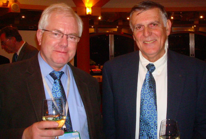
The French scientist Jean-Marie Dubois, PhD in Physics from National Polytechnic Institute of Lorraine (France) is a Distinguished Director of Research at the French National Center for Scientific Research, CNRS (France), where he chairs a committee dedicated to materials chemistry, nanomaterials and processing. He is the former director of Institut Jean Lamour in Nancy (France), a major research institute in field of materials.
His curriculum shows an international scientific trajectory. Dubois holds Honorary Doctorates (Dr Hon. Causa) from Iowa State University (USA) and Federal University of Paraïba (Brazil), is a former “overseas fellow” of Churchill College at University of Cambridge (U.K.) and a permanent visiting professor at Dalian University of Technology (China). He was recently elected as Honorary Member of Jožef Stefan Institute in Ljubljana (Slovenia). He is a member of Lorraine Academy of Sciences (France).
He is the author of more than 250 scientific articles in refereed journals, 14 international patents, and 7 books. His papers were cited more than 5400 times (H index = 39).
Read our interview with the lecturer.
SBPMat newsletter: – Under your viewpoint, which are your main contributions to the field of Materials Science and Engineering? And your scientific/technological contributions with more social impact (patents, products)?

Jean-Marie Dubois: – My first contribution that was aimed at a social impact was the discovery of Al-based metallic glasses, which could be good candidates for light-weight alloys useful for the aeronautic industry. I patented them in 1982, listing a number of favorable examples, and as is the rule for a patent, also counter examples. One such composition was in fact a stable quasicrystal, which was unraveled in Japan few years later. Based on this discovery, I was the first to patent few application niches of quasicrystals that are Al-based intermetallics showing no periodic order as do conventional crystals. The discovery of quasicrystals dates back to 1982, but was published in literature only in 1984, whereas my first patent on these materials was filed in 1988. From that on, I dedicated quite some efforts to discover, patent, and produce new research, about different areas of the physics of quasicrystals including thermal conductivity, adhesion and friction, corrosion resistance, etc. My leadership in this area of materials science is recognized by the international community through the “International Jean-Marie Dubois Award” that is offered every three year “to recognize important, sustained research on any aspect of quasicrystals within the 10-year period preceding the award”. Altogether, I own 14 international patents, with more than 35 extensions. I was responsaible for few tens of collaboration contracts with the industry, including a good dozen of contracts financed by the European Commissions with on average half a dozen of industrial partners and the same number of academic partners. The last one was a so-called Network of Excellence that started the field of Complex Metallic Alloys in Europe, with 20 partner institutions from 12 European countries and some 400 scientists on board.
SBPMat newsletter: – Please choose some of your main publications (about 3 or 4) to share them with our public.
Jean-Marie Dubois:
1) Useful Quasicrystals; J.M. DUBOIS, World Scientific, Singapour (2005), 470 pages.
2) Complex Metallic Alloys, Fundamentals and Applications; Eds. J.M. DUBOIS and E. BELIN-FERRÉ, Wiley (Weinheim, 2010), 409 p.
3) Topological instabilities in metallic lattices and glass formation; J.M. DUBOIS, J. Less Common Metals 145 (1988), 309-326.
4) The applied physics of quasicrystals; J.M. DUBOIS, Scripta Physica, T49 (1993) 17-23.
5) Properties- and applications of complex metallic alloys, J.M. DUBOIS, Chem. Soc. Rev., 41 (2012) 6760-6777.
SBPMat newsletter: – Please give us a short teaser about your plenary talk at SBPMat meeting. What do you intend to broach?
Jean-Marie Dubois: – My talk will be a laudation to the discoverer of quasicrystals who was awarded a Nobel Prize in Chemistry in 2011 for his discovery that forced the scientific community to revise its understanding of ordered condensed matter. Members of the MRS Brazil are used to know what is a crystal, a periodically ordered solid. I wish to introduce them to another type of order in solid, that is not periodic, and leads to unprecedented properties. Alloys that exhibit such a type of order are specific and I call them push-pull alloys. Then, I wish to show that this type of order is not restricted to metallic alloys, but may also be encountered in soft matter like polymers, oxides, artificial nanostructures, and even artistic drawings from ancient Islamic tilings. The talk will therefore be a review for the non-expert in quasicrystals and complex intermetallics
