The scientific paper by members of the Brazilian community on Materials research featured this month is:
T. E. P. Bueno, D. E. Parreiras, G. F. M. Gomes, S. Michea, R. L. Rodríguez-Suárez, M. S. Araújo Filho, W. A. A. Macedo, K. Krambrock and R. Paniago.Noncollinear ferromagnetic easy axes in Py/Ru/FeCo/IrMn spin valves induced by oblique deposition. Appl. Phys. Lett. 104, 242404 (2014). DOI: 10.1063/1.4883886.
Accurate engineering in spin valves manufacturing
The production and characterization of spin valves is the theme of a collaborative work between Brazil and Chile, whose results were published recently in the prestigious journal Applied Physics Letters (APL).
Spin valves are devices consisting of three or more layers of nanometric thickness composing a sandwich of magnetic and non-magnetic materials. Sensors consisting of such structures fulfill a fundamental role in reading the information written on the hard disc drives, among other applications.
The operation of spin valves is based on an effect called “giant magnetoresistance”, which was the reason behind the Nobel Prize in Physics in 2007. The giant magnetoresistance of spin valve consists of a large change in the electrical resistance in response to the action of a magnetic field. This resistance depends on the relative orientation among the magnetization of the magnetic material layers.
The magnetization of a magnetic material is determined by the orientation of the spins of its electrons. Electrons have two intrinsic features: electric charge and magnetic moment, the latter known as spin. Explore the degree of freedom of the electron spin in addition to its charge led to the emergence of a new field of research called spintronics.
Then, on giant magnetoresistance of spin valves, when the layers of magnetic material have the same direction of magnetization, the device reduces its electrical resistance and becomes a better conductor of electricity. When the magnetic layers acquire opposite directions of magnetization, a significant increase of electrical resistance occurs.
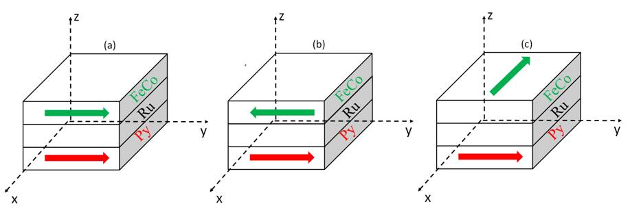
For better understand this effect and, later, the results presented in the article of APL, it is important to remember that the magnetization is a vector physical quantity and that, therefore, besides having an intensity, it has a direction (parallel, perpendicular) and an orientation (indicated by the arrowhead representing the vector). Usually, metallic multilayers composed of magnetic materials separated by a non-magnetic layer, as spin valves, have the magnetization of ferromagnetic layers coupled, says Thiago Bueno, first author of the APL article and PhD student in Physics at the Brazilian Federal University of Minas Gerais (UFMG), supervised by professor Roberto Magalhães Padilla. This coupling can result in parallel magnetization (called “collinear”) with same or opposite orientations, and also in non-collinear magnetization.

However, to magnetize the magnetic layers of the spin valve does not occur homogeneously in all directions; they feature the so-called magnetic anisotropy. “The magnetic anisotropy is an important magnetic property, because it establishes an easy direction of magnetization,” says Thiago Bueno. “This property is determined by a number of factors, including the types of materials, the thickness of layers, and the details of the method of sample manufacturing”.
On the work that originated the APL article, the team of scientists has made some adjustments to the method of spin valves manufacturing, obtaining interesting results on the properties of these devices.
Controlling the direction of magnetization
“This work was only possible due to the great collaboration between the parties along the preparation of samples of excellent quality, accurate experimental measures, interpretation of the data, until the publication of the results,” says Thiago Bueno.
Initially, at the Brazilian Center for Development of Nuclear Technology (CDTN in Portuguese) the team has made thin films composed of multi-layers with thickness of a few tens of nanometers. The films were obtained through the technique known as magnetron sputtering, in which argon ions are accelerated against the targets that contain the materials to be deposited, ripping off its atoms. With the aid of magnetrons, these atoms are deposited on a substrate, forming the layers of films. “Through this technique it is possible to obtain films with well-determined chemical composition, thickness and structural morphology,” says Thiago Bueno.

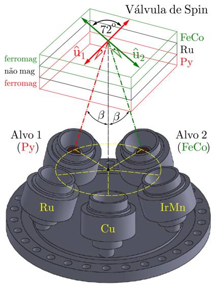
In this study, the scientists set up an oblique deposition scheme by putting the magnetrons making an angle of 72o between them and inclined towards the sample. Using the oblique deposition scheme, scientists made spin valves with ferromagnetic layers up to 10nm-thickness, composed of metallic alloys (Py and FeCo), and separated by a non-magnetic layer of ruthenium (Ru) of thickness between 1nm and 3.5nm. The devices were characterized in the Physics Department at UFMG using ferromagnetic resonance (FMR), an extremely sensitive technique that provides relevant information on the magnetization of materials.
After the interpretation of experimental results, which involved researchers from the Pontifical Catholic University of Chile, the scientists concluded that the oblique deposition induced non-parallel magnetization directions (non-collinear) on ferromagnetic layers of manufactured spin valves. “The angle between the easy axes, approximately equal to the angle between the magnetrons, was determined by the manufacturing geometry”, reinforces the author, Bueno. “One of the main contributions of our work is the demonstration that it is possible to manufacture spin valves where the axes of easy magnetization of ferromagnetic layers (Py and FeCo) are non-collinear,” he sums up.
According to the doctoral student, at the beginning of the work the authors already knew the oblique deposition effects in ferromagnetic/anti-ferromagnetic bilayers. With this study, the team took a step further and has investigated these effects in a more complex structure, the spin valve.
“We believe that our work will compel other researchers into manufacturing these devices, seeking new magnetic configurations between layers of the spin valve “, says Bueno.

