The scientific paper by members of the Brazilian community on Materials research featured this month is:
Archanjo, B.S.; Fragneaud, B.; Cancado, L.G.; Winston, D.; Miao, F.; Achete, C.A.; Medeiros-Ribeiro, G. Graphene nanoribbon superlattices fabricated via He ion lithography. Appl. Phys. Lett. 104, 193114 (2014); http://dx.doi.org/10.1063/1.4878407.
Graphene sheets engraved with helium ions
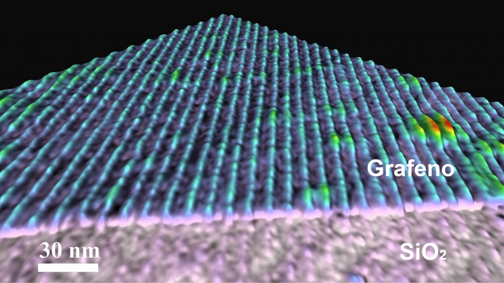
In a study led by researchers from Brazil and recently published in Applied Physics Letters (APL), scientists have engraved, on graphene sheets, nanosized periodic patterns, using a new method for that application, the helium hion beam lithography.
The team of scientists used a helium ion microscope (HIM) in order to bombard graphene with these ions and, thus, engrave parallel lines of length 1mm and width of only 5 nm, defining, among them, 20 nm-width ribbons (nanoribbons).
In addition to being quick and simple, the method has proven to be very accurate: it generated point defects smaller than other similar techniques and significantly preserved the atomic structure of the nanoribbons.
The new method extends the application possibilities of graphene, which, it is worth highlighting, is a flat material (it is only one atom tall) composed of densely packed carbon atoms, and which stands out because it can be used in nanoscale and for its high mechanical resistance, great electricity and heat conduction, transparency, and flexibility, among other properties.
“Direct writing in graphene using the focused beams of helium ions allows the fast manufacturing of different devices”, says Braulio Archanjo, researcher at the Brazilian National Institute of Metrology, Quality, and Technology (Inmetro) and lead author of the APL’s article. As an example, Archanjo mentions the possibility of manufacturing, in a near future, in pure graphene, the so-called “PN junctions”, essencial structures in semiconductor devices such as diodes and transistors, widely used in the production of electronics. Today, these structures are basically made in silicon.

The story of the work
In the context of studies on graphene metrology performed in the recent years at Inmetro, reports Archanjo, emerged the idea of manufacturing, in a controlled manner, periodic “defect” patterns, such as the parallel lines of the APL work. In 2012, an Inmetro team, in collaboration with researchers of the Federal University of Minas Gerais (UFMG), published a paper on periodic patterns engraved on graphene using a beam of gallium ions through FIB (focused ion beam) equipment.
Later, in a meeting of Archanjo with professors Carlos Achete, from the Federal University of Rio de Janeiro (UFRJ) and from Inmetro, and Gilberto Medeiros, from UFMG and from the research and development laboratory of Hewlett-Packard (HP Labs), a second work was planned, which would use, instead of FIB equipment, a HIM equipment, which resolution is up to ten times higher, but which is still not available in Brazilian territory.
So Archanjo spent three weeks in Silicon Valley, in the United States, using the HIM of HP Labs to make lithography in graphene samples manufactured at Inmetro. “We brought together the expertise we have here regarding graphene defects with the expertise of the HP Labs researchers regarding using a microscope of focused beams of helium ions”, summarizes the Inmetro researcher.
When he went back to Brazil with several graphene samples with engraved periodic patterns, the team began, at Inmetro, the study of such samples through atomic force microscopy and Raman spectroscopy. “This stage of the work was performed together with professors Benjamin Fragneaud, from the Federal University of Juiz de Fora (UFJF) and Luiz Gustavo Cançado, from UFMG”, tells Archanjo.
HIM: soon in Brazil
In the first semester of 2015, announces Archanjo, Brazil should have its first helium ion microscope. “The experience we gained performing the study at HP Labs will allow us to install it and use it”, says the researcher. The equipment will be available at Inmetro.
