[Paper: Direct Drawing Method of Graphite onto Paper for High-Performance Flexible Electrochemical Sensors. Santhiago, Murilo; Strauss, Mathias; Pereira, Mariane P.; Chagas, Andreia S.; Bufon, Carlos C. B. ACS Appl. Mater. Interfaces, 2017, 9 (13), pp 11959–11966. DOI: 10.1021/acsami.6b15646]
Pencil and paper to make an electrochemical sensor
Perhaps many of us have not thought of this before: painting a paper sheet with a graphite pencil creates, in addition to a drawing, a layer of electrically conductive material (graphite, made up of carbon atoms) on a flexible, inexpensive and widely available substrate (the paper). In other words, this extremely simple and quick method produces a very attractive platform for manufacturing sensors and other devices.
Based on this method of transferring graphite from pencil to paper, a team of Brazilian scientists developed a flexible electrochemical sensor. The device showed exceptional performance among similar sensors in the detection of a biological compound that is very difficult to detect , but also very relevant because it is present in all cells, fulfilling important functions in the metabolism of living beings.
The work was mostly carried out in the Brazilian Nanotechnology National Laboratory (LNNano) of the National Center for Research in Energy and Materials (CNPEM). Some analyses were conducted at the Multiuser Laboratory of Advanced Optical Spectroscopy of the Institute of Chemistry of UNICAMP, the State University of Campinas.
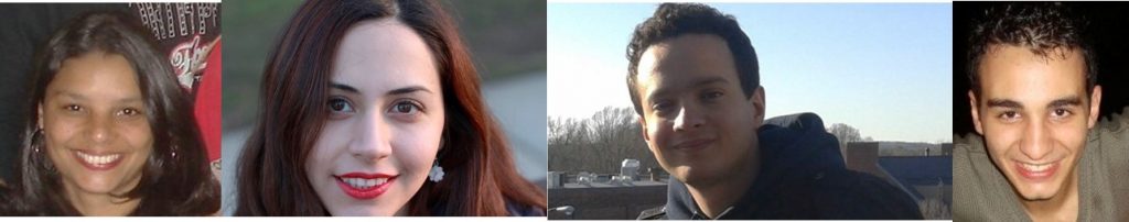
Researchers of the Laboratory of Functional Devices and Systems (LNNano/CNPEM): the coordinator Carlos Bufon (left) and Murilo Santhiago.
“One of the main contributions of the work was to show the efficiency of electrochemical devices prepared through a process of direct transfer of graphite on paper,” points out Carlos César Bof Bufon, corresponding author of a scientific article about the study, which was recently published in the journal ACS Applied Materials and Interfaces (impact factor = 7,504). Prof. Bufon and Dr. Murilo Santhiago lead the study, and all the authors are researchers of the Laboratory of Functional Devices and Systems at LNNano/CNPEM.
The work began with the aim of manufacturing carbon and/or hybrid electrochemical devices that would efficiently detect biological compounds, says Bufon. A survey of scientific literature showed the team of scientists that various types of carbon electrodes prepared through a wide variety of methods had already been reported, and that they all exchanged electrons very slowly when tested with some model molecules. In other words, for biological molecules they were not efficient electrochemical sensors. The team then chose the simplest carbon electrode preparation method (the pencil drawing) and decided to investigate why the material obtained did not show good results when used as an electrochemical sensor of these molecules. “We then decided to work on this issue by mapping the problems observed in other works and improving the aspects regarding the graphite surface”, states Santhiago.
The team was able to verify, for example, that the process of transferring graphite from pencil to paper left micro and nano debris on the surface of the electrode. To remove them, the researchers performed a quick electrochemical treatment on the electrode, which generated oxygen bubbles on the surface, which helped remove the debris and other impurities from the carbon film and push them away. “After this treatment, we found that the sensor response was one of the best for this type of material”, says Santhiago. To explain the exceptional performance, the scientists analyzed the carbon film before and after treatment using different materials characterization techniques and found that the electrochemical treatment generated changes in the structure and chemical composition of the carbon film surface.
After optimizing the paper-based carbon electrode, the team tested its ability to detect biological molecules and chose nicotinamide-adenine dinucleotide (NAD) as the analyte. This molecule is often used in tests, not only because of its relevance (it participates in more than 300 biological processes), but also because of the challenges of its detection. Therefore, the scientists had to make some adjustments in the electrode in order to make it more selective (to only detect NAD) and more sensitive (to detect small amounts of the molecule).
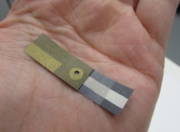
Picture of the paper-based electrochemical sensor.
Then, the scientific team inserted on the surface of the electrode a compound that facilitates the transfer of electrons, the dye Meldola`s Blue. In the NAD detection tests, the final version of the sensor showed excellent performance, presenting the best results so far reported regarding the selectivity and speed of detection among paper-based electrodes. “Now, the simplest method is also the most efficient one, the one with the greatest application potential”, concludes Murilo Santhiago.
Following the success of manufacturing high-efficiency pencil-based graphite electrodes, the team continued its research on the subject. The scientists are now studying other applications of the material in electrochemical devices, including wearable ones, for the detection of species of biological and environmental interest. They are simultaneously working on the scalability of the manufacturing process to minimize small variations between devices – not a trivial point when we consider that the method is based on the manual use of a graphite pencil, among other manual processes. “Achieving scalability and high-efficiency materials at the same time is not always an easy task”, says Bufon, citing the example of graphene, which was initially isolated using adhesive tape through a simple and manual process, and with reproducibility problems.
The research was funded by CNPq and FAPESP, and used the infrastructure of the Brazilian National System of Nanotechnology Laboratories (SisNANO) at LNNano.
Until August 14, undergratudate and graduate students who are authors of accepted abstracts can apply for the student awards of the XVI B-MRS Meeting. In addition to the traditional “Bernhard Gross Award” from the Brazilian Materials Research Society, this edition of the event will feature awards from the publisher of the American Chemical Society (ACS Publications), responsible for a number of very prestigious peer-reviewed scientific journals in the materials field.
The Bernhard Gross Award was established by SBPMat in honor of the pioneer of Brazilian materials research Bernhard Gross, and it distinguish the best works (up to 1 oral and 1 poster) from each symposium.
Among the winners of the Bernhard Gross Award, the three best posters and the three best oral presentations will receive the “ACS Publications Best Poster Prize” and the “ACS Publications Best Oral Presentation Prize” respectively. The prizes will consist of US $ 500 for each winning work, in addition to the certificate. The ACS awards will be sponsored by the following ACS’s journals: ACS Applied Materials & Interfaces, ACS Nano, Nano Letters, Chemistry of Materials, JACS and ACS Omega.
In order to compete for the prizes, students have to submit through the website of the event, an extended abstract, elaborated according to the template that is available in the instructions for authors.
The papers will be evaluated considering the quality of the extended abstracts and presentations, as well as the scientific contribution of the research work.
The Student Awards Ceremony will take place at the closing of the XVI B-MRS Meeting, on September 14. Prizes will only be given if the winner students are present at the ceremony.
Six ACS journals will sponsor the prizes for the best student contributions.
The newsletter of the Brazilian Materials Research SocietyNews update from Brazil for the Materials community
English edition. Year 4, issue 5.
XVI B-MRS Meeting (Gramado, Brazil, September 10-14)
Approximately 2,000 abstracts were submitted to the XVI B-MRS Meeting!
Authors. The authors will be notified by June 20 on the acceptance, modification or rejection of submitted papers.
Registration – discounts. Registrations are open. All categories have discounts until August 31st. See here the different values for B-MRS members (you can become a member during registration) and for non-members. And see here other advantages of joining SBPMat.
Students Awards. Contributions submitted by authors who are undergraduate or graduate students can apply for the students awards (the Bernhard Gross Award from B-MRS and other awards from partner entities). To participate in the selection, the author must submit an extended abstract in addition to the conventional abstract. The deadline is August 14. Additional information in the instructions for authors, here.
Plenary lectures. Seven internationally renowned scientists will speak about cutting edge research on subjects such as materials for biomedical and environmental applications; biomimetic surfaces;
heterogeneous catalysis; materials and technologies for miniaturized electronic circuits; piezoelectric films and their energy, optics and electronics applications. Learn more by clicking on the speakers’
photos, here.
Memorial lecture. At the opening of the event, SBPMat will pay homage to Professor João Alziro H. da Jornada, from the Federal University of Rio Grande do Sul (UFRGS), who will deliver the
traditional Memorial Lecture “Joaquim da Costa Ribeiro”.
Venue. The FAURGS event center is in the center of Gramado, within walking distance of restaurants, shops, tourist attraction spots and hotels.
City of the event. Gramado is a charming tourist town, with a wide and qualified chain of hotels, gastronomic restaurants and shops. This attractive city is also the starting point for a series of
sightseeing highlights that explores the area’s natural florid beauty, its history marked by German and Italian immigration, and the theme parks around the city.
Organization. Meet the organizing committee. Here.
Exhibitors.21 companies have already confirmed their participation in the industrial exhibition. Some booths are available. Companies interested in participating in the event with booths and other means of dissemination should contact Alexandre via this e-mail: comercial@sbpmat.org.br.
Mini-interviews with the plenary speakers of the event. Professor Hans-Joachim Freund, known as Hajo Freund, is a German scientist who heads, since 1996, a prestigious research institute in Berlin dedicated to the study of surfaces and interfaces. There, he also heads a group of more than 40 people devoted to understanding heterogeneous catalysis through the study of model catalysts. In Gramado, this scientist, who has a 97 h-index, will share with the audience his knowledge on heterogeneous catalysis, a theme of broad academic and industrial impact. See our mini-interview.
B-MRS news
Young Research Award. B-MRS announced the results of its post-doc award, this year in partnership with E-MRS. The four young winners, selected from 20 candidates, will take part in international events in Strasbourg (France). Learn more about this.
Save the date. B-MRS announces that the 17th edition of its annual event (XVII B-MRS Meeting) will be held in the city of Natal (Rio Grande do Norte state), at the Convention Center of Praiamar Hotel, on September 16 – 20, 2018, under the coordination of Professor Antonio Eduardo Martinelli (UFRN).
Featured paper
A team of scientists was able to produce a hybrid material made of graphene oxide nanosheets and iron oxide nanoparticles with a special 3-dimensional morphology. The work was carried out at the Center for Semiconductor Components at UNICAMP and at an Indian university. When the material performance in electricity storage was tested, the hybrid proved to be promising as a flexible micro-supercapacitor for wearable electronics. The research was reported in ACS Applied Materials & Interfaces. See our news story.
People from our community
We interviewed the new director of the Brazilian Nanotechnology National Lab (LNNano), Adalberto Fazzio, former president of SBF, former pro tempore president of the Federal University of ABC and former coordinator of micro and nanotechnologies of the Brazilian Ministry of Science, among other management positions. Fazzio was a Professor at the Physics Institute of USP from 1979 until his retirement in 2015, and made significant contributions to the understanding of various materials (from semiconductors to topological insulators) using computational methods. In the 1980s and 1990s, Fazzio pioneered the use of ab initio calculations in Brazil and is currently exploring the use of machine learning techniques to study materials properties. In the interview, Prof. Fazzio spoke about his professional trajectory and the perspectives in nano research in light of today`s Brazilian budget situation. He also left a message for the readers who are starting their scientific careers. See the interview.
Reading tips
Method that aggregates real-time observation and computational modeling of piezoelectric material reveals details of nano-scale power generation mechanism (based on paper from Nano Letters). Here.
Nanoparticle functionalized with antibiotic developed in Brazil kills bacteria resistant to this antibiotic (based on paper from Scientific Reports). Here.
Sensor created in Brazil evaluates ethanol fuel quality in seconds with more precision than the sensors currently used (based on paper from Scientific Reports). Here.
Technology: Brazilian company develops electrostatic protection materials applicable to flooring, packaging, soles, carpeting and other products. Here.
Events
9th International Conference on Materials for Advanced Technologies. Suntec (Singapore). June 18 – 23, 2017. Site.
10th International Conference on Nanophotonics (ICNP 2017). Recife, PE (Brazil). July 2 – 5 2017. Site.
1ª Escola Brasileira de Síncrotron (EBS). Campinas, SP (Brazil). July 10 – 21, 2017. Site.
2º Ciclo de Minicursos de Cristalografia. Juiz de Fora, MG (Brazil). July,10 – 21, 2017. Site.
XI Brazilian Symposium on Glass and Related Materials (XI Brazglass). Curitiba, PR (Brazil). July 13 – 16, 2017. Site.
VIII Método Rietveld de Refinamento de Estrutura. Fortaleza, CE (Brazil). July 24 – 28, 2017. Site.
XXXVIII Congresso Brasileiro de Aplicações de Vácuo na Indústria e na Ciência (CBRAVIC) + III Workshop de Tratamento e Modificação de Superfícies (WTMS). São José dos Campos (Brazil). August 21 – 25, 2017. Site.
International Conference on Luminescence (ICL-2017). João Pessoa (Brazil). August 27 – September 1, 2017. Site.
23a Reunião da Associação Brasileira de Cristalografia. Vitória, ES (Brazil). September 5 – 9 2017. Site.
XVI Encontro da SBPMat/ XVI B-MRS Meeting. Gramado, RS (Brazil). September 10 – 14, 2017. Site.
18th International Conference on Internal Friction and Mechanical Spectroscopy (ICIFMS-18). Foz do Iguaçu, PR (Brazil). September 12 – 15 2017.Site.
2ª Conferência Nacional em Materiais Celulares (MatCel’2017) + Conferência Internacional em Dinâmica de Materiais Celulares (DynMatCel’2017). Aveiro (Portugal). September 25 – 27, 2017. Site.
1st Pan American Congress of Nanotechnology. Fundamentals and Applications to Shape the Future. Guarujá, SP (Brazil). November 7 – 30 2017. Site.
Submit your suggestion for any section of our newsletter: comunicacao@sbpmat.org.br
Since April of this year, the Brazilian Nanotechnology National Laboratory (LNNano) of the National Center for Research in Energy and Materials (CNPEM) is headed by the scientist Adalberto Fazzio, 66, born in the São Paulo state city of Sorocaba.
Adalberto Fazzio has been studying materials through computational tools for over four decades. He pioneered in Brazil the use of ab initio calculations, widely used in the study of materials properties, and made significant contributions toward understanding transition metals, amorphous systems, gold (Au) and silver (Ag) thin films, carbon nanostructures, silicon, topological insulators, and other materials. Fazzio and his research group, known as SAMPA (acronym for “Simulations Applied to Atomic Materials and Properties”), have successfully worked on this at the Institute of Physics of the University of São Paulo (USP) and also with several theoretical and experimental collaborators from Brazil and abroad.
Adalberto Fazzio received his undergraduate (1972) and master’s degree (1975) in Physics at the University of Brasília (UnB) and his doctorate (1978),also in Physics, at USP.
Fazzio became a professor at the Institute of Physics – USP in 1979, shortly after completing his doctorate. In 1985 he became an associate professor at that university and in 1991 he became full professor. He was a visiting researcher at the National Renewable Energy Laboratory (USA) from 1983 to 1984 and at the Fritz-Haber-Institut der Max-Planck-Gesellschaft (Germany) from 1989 to 1990. In May 2015, he retired from USP. He was a visiting Professor at the Brazilian Federal University of ABC (UFABC) in 2016.
Throughout his career, Fazzio has held several management positions, such as president of the Brazilian Society of Physics (SBF) from 2003 to 2007; pro tempore president of UFABC from 2008 to 2010; micro and nanotechnologies general coordinator at the Ministry of Science, Technology and Innovation (MCTI) in 2011; assistant secretary of the Technology, Development and Innovation Secretariat of MCTI from 2011 to 2013, and director of the Institute of Physics – USP from 2014 to 2015.
He has also received other honors, such as the Brazilian National Order of Scientific Merit in 2006 (promoted to the Grand-Cross class in 2010). In 2013 he was elected a fellow of TWAS (The World Academy of Sciences). He is a member of several scientific societies, such as the Brazilian Academy of Sciences and the Academy of Sciences of the State of São Paulo in Brazil, and the American Physical Society, American Chemical Society and Materials Research Society in the United States.
Fazzio is the author of over 270 articles published in indexed scientific journals. His scientific production has about 8,000 citations, according to Google Scholar. He has supervised approximately 40 master’s and doctoral students.
Here is an interview with the scientist.
SBPMat Bulletin: Tell us what led you to become a scientist and in particular to work in the area of Condensed Matter Physics.
Adalberto Fazzio: When I finished my Physics course at the University of Brasilia in 1972, I met Professor José David Mangueira Vianna, who had returned from Switzerland with many projects on Molecular Physics. At that time we were talking about quantum chemistry. He presented a master’s project that was an improvement on semi-empirical models based on the Hartree-Fock method. Due to the low computational capacity of that time, these methods originating from the ZDO (Zero Differential Overlap) approximation were the most widely used to shed light on the electronic properties of molecules. After my master’s degree, I went to the Institute of Physics – USP in the group of Professors Guimarães Ferreira and José Roberto Leite (my doctoral advisor), changing from molecules to solids and from Hartree-Fock to DFT (Density Functional Theory). At that moment I became a Condensed Matter Physicist in a Department of Physics of Materials created by Professor Mário Schemberg. My thesis was about deep level impurities in semiconductors. Bear in mind this was in 1976 and the question was how to treat a crystal that has lost its translational symmetry. Finally, I developed a model, “Molecular Cluster Model for Impurities in Covalent Semiconductors.”
SBPMat Bulletin: What do you believe are your main contributions to the Materials area? We would like to ask you to go beyond listing the results and to briefly describe the contributions you consider as the most relevant. In your response, we ask that you consider all aspects of scientific activity. Feel free to share references to articles and books, if relevant.
Adalberto Fazzio: Whenever we reflect on the main contributions in a given area, we look at the most cited articles, which do not always correspond to the articles that the authors would expect to be the most cited. But I will try to give you a brief description of some of the themes in which I believe I made a contribution that was highlighted. In the study of defects and impurities in semiconductors, I highlight the study of transition metals (TM) in semiconductors. At the time – until 1984 – there was a wealth of experimental data concerning the position of levels of impurities in the gap and the optical excitations of all MT-3ds. And the theoretical calculations based on a medium-field theory did not explain these data. During my post doctoral research at NREL (National Renewable Energy Laboratory) in 1983/84, we developed a model to describe the experimental data. It was a model that coupled the field crystal theory with the DFT theory, which described effects of multiplets from the TM impurities. Several articles were published applying this model. The model is presented in detail in Phys. Rev. B 30, 3430 (84). This work was in collaboration with the researchers Alex Zunger and Marilia Caldas. And those results led to a letter in the Appl. Phys. Lett. (1984) which would be of great interest to experimental physicists, titled “A Universal trend in the binding energies of deep impurities in semiconductors”. A major change occurred in this area in the late 1980s, with the “Large Unit Cell” calculations, DFT method and pseudo potentials. Today known simply as “ab initio methods” or “free parameters”. Regarding this development, I was at the Max Planck Institute in Berlin, working with Matthias Scheffler. Together with my doctoral students (T. Schmidt and P. Venezuela), we were pioneers in the use of this type of methodology in Brazil, widely used until now. After these studies, I started working with amorphous systems. Since we could now work with systems containing many atoms per unit cell, we decided to couple the ab initio calculations using structures generated by Monte Carlo simulations. I highlight two papers: one in a-SiN (PRB, 58, 8323 (1998)) and a-Ge:N (PRL 77, 546 (96)).
At the end of the 1990s, at the Brazilian National Synchrotron Light Laboratory (LNLS), Professor Daniel Ugarte was performing beautiful experiments with HTEM, where he observed the formation of linear chains of atoms in Au and Ag fine films. Our group at USP, in cooperation with Edison Zacarias at UNICAMP, had begun studies to understand the formation of linear chains of Au atoms. Some of the questions were about how these chains broke and how we could explain the great distances that appeared between atoms. This experiment-theory interaction was a very important moment. Several papers were published, one which was widely cited “How do gold nanowire break?” (PRL 87, 196803 (2001)). This work was the cover of PRL and highlighted by the editor of Science. And later we showed how oxygen acts to trap the Au atoms in the wires (PRL 96, 01604 (2006)) and the effects of temperature and quantum effects on wire breakage and stability, important aspects to understand the observations (PRL 100, 0561049 (2008)).
In the same period, our group at USP focused on the study of nanostructures of carbon, silicon, etc. Although we had strong tools for describing electronic, magnetic, optical and mechanical properties, the understanding of these materials lacked the properties of electronic transport. In this context, we developed a computational code based on the Landauer-Büttiker theory. Several PhD students were involved in this code, which is known as TRANSAMPA. And, in my opinion, several important works were carried out to better understand the behavior of electronic transport properties. To exemplify this, we were pioneers in describing the transport in doped graphene tapes (PRL 98,196803 (2007)). I should also mention the collaboration with Professor Alexandre Reilly from IFT (Institute of Theoretical Physics of UNESP) who was then a post-doc, which resulted in a very important improvement of this code, and which allowed to treat materials with the realistic dimensions used in the experiments. In 2008, in a paper titled “Designing Real Nanotube-based Gas Sensor” (PRL 100, 176803), we showed how nanotubes can function as realistic-sized sensors, with defects. Using first-principle calculations, we had systems of micrometric dimensions within our reach.
Currently, my research is more focused on the search for devices formed by 2D materials whose interface is primarily built by van der Waals interactions. For example, like graphene, a new 2D material was isolated from exfoliated black phosphorus, also called phosphorene. We studied the graphene/phosphorene interface (PRL 114, 066803(20015)), showing how a device can be constructed.
Another class of materials I have been working on concerns the well-known topological insulators. A Topological Insulator (TI) is a material that has no states of energy gap “at the edges” and whose “bulk” is insulating! These states are topologically protected and robust against disturbances. In the case of two-dimensional (2D) materials (2D), they are known as insulators that feature Quantum Spin Hall (QSH). The scattering surface state is protected by time reversal (TR) symmetry, leading to an electronic transport without energy dissipation. In 2011, together with the UFU group, we showed how magnetic impurities in topological insulators have their spin texture modified (PRB 84, 245418 (2011)). Recently, in collaboration with Professor Zhang from the Rensseler Polytecnic Institute, we presented a general model for describing the topological/trivial interface. We showed, for example, the Bi2Se3/GaAs interface. There were replicas of the Dirac cone that emerged from the interface interaction including semiconductor states (Nature Comm. 6, 7630(2015)). Phosphorene is a 2D material that has semiconducting properties. In cooperation with the group of Professot Alez Zunger, of the University of Colorado, we studied this material under the action of an electric field and showed that for three or four layers of phosphorene, under the action of the field, it has a topological transition (NanoLett. 15, 1222 (2015)).
Finally, I would like to mention an activity that I am initiating, which is the use of Machine-Learning techniques for material properties. In particular, I have focused on topological insulators. And as I mentioned earlier, specifying the more relevant studies I have left out many others.
As for other types of contributions, together with José Roque I built a very productive group at IF-USP, known as SAMPA (Simulation Applied to Materials – Atomic Properties) where numerous doctors and masters, and several postdocs were cultivated. I should add that all this was possible mainly due to the support of Fapesp, via thematic projects. I was head of the Department of Materials Physics, Director of IFUSP and pro tempore Director of the Federal University of ABC. From a management point of view, I would like to highlight my participation at the Ministry of Science, Technology and Innovation, where I was the Under-Secretary of Setec (Technology and Innovation Secretariat) and SCUP (Secretariat of Research Units). And I am proud to have coordinated the creation of the Brazilian Nanotechnology Initiative, where the SISNANO system is an important arm – a set of laboratories dedicated to technological research and development.
I also wrote two books that have been adopted: “Introduction to Group Theory: applied in molecules and solids”, together with Kazunori Watari and “Quantum Theory of Molecules and Solids”, together with José David Vianna and Sylvio Canuto.
SBPMat Bulletin: You have just taken on the direction of the Brazilian National Nanotechnology Laboratory (LNNano). Please share with the Materials community your plans for LNNano. How do you see the situation of nanoscience and nanotechnology research in Brazil given the recent budget cuts?
Adalberto Fazzio: Two weeks ago I took on the direction of the National Nanotechnology Laboratory (LNNano), one of the four National Laboratories of the National Center for Research in Energy and Materials (CNPEM). This is a laboratory recognized for its excellence, dedicated to the production of knowledge in nanotechnology, moving from basic science to technological innovation.
I was very happy and I hope to continue the work of the researchers who were at the forefront of LNNano and who preceded me, such as Daniel Ugarte, Fernando Galembeck and Marcelo Knobel. This is the laboratory that holds a management bond with MCTIC fully dedicated to nanotechnology. One of its main missions is to service external users through open equipment. An example is the electron microscopy and probes park, which is certainly the best equipped in Latin America. LNNano is the main executor of government policies in the area. We have intense in-house mission-oriented research activity with impact studies. We are currently undertaking minor restructurings to better serve external users and to strengthen ongoing research.
The nanotechnology platform has raised considerable resources in all developed countries of the world. For example, the US government has annually deposited something in the order of US$ 1.8 Bi. Unfortunately, in Brazil we have had difficulties to provide continuity to even much more modest programs. However, the community has responded with great capability to the development of nanotechnology products. Today, for example, anchored in the SISNANO system, we have about 200 companies seeking innovation in the Nano area; and in particular, the performance of LNNano has been outstanding.
What we cannot however, is face budget cuts in science and technology every year. We are in a very delicate moment in our economy, low growth, but it is imperative to preserve the achievements of the last decades in the area of science and technology. The programs in the area of research and technology development must be preserved. This is because when the crisis is over, the country must be prepared to continue growing. Therefore, it is fundamental to continue generating new knowledge, striving for technological innovation and also training qualified human resources. In other words, the economic slowdown should not be accompanied by investment cuts in technology and development research.
SBPMat Bulletin: Please leave a message for the readers who are starting their scientific careers.
Adalberto Fazzio: The greatest wealth in our country is human capital. Brazil has a large young population, young people who are often in the middle of the path in their scientific and technological careers, because they are not able to envision in the future the acknowledgment and respect for a fundamental activity, which is the search for knowledge. Those who desire to pursue a scientific career must persevere and stand firm in their studies.
B-MRS (Brazilian Materials Research Society) announces the list of winners of “Young Researcher Award” (YRA), an award from the Society bestowed on postdoctoral fellows, this year in partnership with E-MRS (European Materials Research Society).
The winners are:
Gisele Amaral-Labat (USP – Department of Metallurgical Engineering and Materials)
Seyedeh Parinaz Akhlaghi (UNICAMP – Institute of Chemistry)
Kassio Papi Silva Zanoni (USP – São Carlos Institute of Physics)
Eduardo Guilherme Cividini Neiva (UFPR – Department of Chemistry)
The prize winners: Gisele Amaral-Labat, Seyedeh Parinaz Akhlaghi, Kassio Papi Silva Zanoni and Eduardo Guilherme Cividini Neiva.
The prize winners will participate in two invitation-only international events: “Forum for the Next Generation of Researchers 2017” (Strasbourg, France, 18-19 November 2017) and “6th World Materials Summit” (Strasbourg, France, 20-21 November 2017). They will have travel expenses covered.
SBPMat is grateful to all the candidates participating and congratulates those selected, wishing them a fruitful participation at the events.
Judging Committee
The winners were selected from 20 postdocs who submitted their applications by March 31 of this year. The selection of the YRA winners considered the eligibility criteria explained in the edict, the evaluation of the abstracts of the work to be presented in the events and the evaluation of the CV.
SBPMat thanks the judging committee, consisting of Professors Christoph Deneke, Iêda Maria Garcia dos Santos and Newton Barbosa.
 Pencil and paper to make an electrochemical sensor