Online registration for the XVIII B-MRS Meeting (Balneário Camboriú, September 22 to 26, 2019) is open.
Early registration (with descount) is open by August 2 August 9. Onsite registration at the event venue (Hotel Sibara) will be available throughout the meeting.
For participants of Brazilian institutions, B-MRS members benefit from additional discounts, and it is possible to become a B-MRS member or renew membership at the moment of meeting registration (online or onsite).
Newsletter of the
Brazilian Materials
Research Society
Year 6, issue 6. July 8, 2019.
B-MRS News
– XVIII B-MRS Meeting (Balneário Camboriú, September 22-26, 2019). The program of the event, at a glance, is already on the website. See here. Additionally, submission of extended abstracts to compete for student awards is open. Learn more about the awards here.
– XIX B-MRS Meeting (Foz do Iguaçu, August 30 to September 3, 2020). The event will be held together with the International Conference on Electronic Materials IUMRS – ICEM. The event site is already online. See here. In addition, the call for symposia proposals for the event is open until October 31, 2019. Access the symposia submission form, here.
– International Year of the Periodic Table. The International Union of Materials Research Societies (IUMRS), of which B-MRS is a member, endorses the International Year of the Periodic Table (UNESCO). Know more.
Featured Paper
A Brazilian scientific team has shown, through computer simulations, a way to control the electronic properties of a graphene sheet and its silicon-based substrate. The study, which was reported in Carbon, can contribute to the development of two-dimensional electronic devices. Know more.
Featured Scientist
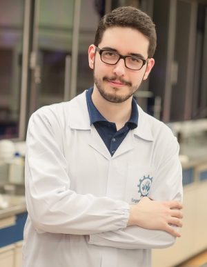
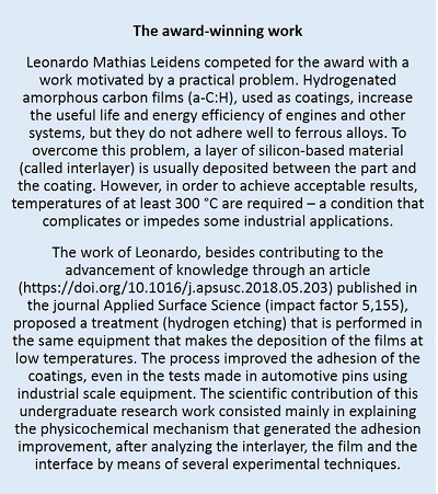
We interviewed Leonardo Mathias Leidens, winner of the Brazilian national award for the best undergraduate research in the area of Exact, Earth and Engineering Sciences. This young student, recently graduated in Chemical Engineering and a PhD candidate in Materials Science at the University of Caxias do Sul (Brazil), has studied the adhesion of amorphous carbon films in ferrous alloys, culminating in an industrial treatment that increases adhesion, and a model of the physicochemical mechanism that generates the improvement. See our interview.
News from B-MRS Members
– B-MRS members are editors of a MRS journal focus issue on nanomaterials for biomedical applications. Know more.
Community
– B-MRS expresses deep regret over the death of Eloisa Biasotto Mano, Emeritus Professor at UFRJ (Brazil). Professor Eloisa died on June 8, 2019, at the age of 94. She was honored by B-MRS in 2015 with the “Joaquim da Costa Ribeiro Memorial Lecture”. See the biographical article about Professor Biasotto Mano published in the 2015 B-MRS Bulletin, here.
XVIII B-MRS Meeting
(Balneário Camboriú, SC, Brazil, September 22 – 26, 2019)
Program. The program of the event “at a glance” is online, with its technical and social activities.See here.
Awards for students. To apply for awards for undergraduate and graduate students (Bernhard Gross Award and ACS Publications Prizes), authors are required to submit an extended abstract by July 14. Learn more, here.
Posters printing service. The poster file can be sent by email and later pick up the impression at the event location. Know more, here.
Venue. The meeting will be held in the delightful Balneário Camboriú at the Hotel Sibara Flat & Conventions, located in the center of the city, close to many hotels, restaurants and shops, and only 100 meters from the sea. More information, here.
Opening ceremony venue. The opening ceremony, the memorial lecture and the welcome cocktail will be held on September 22 (Sunday) at the Cristo Luz complex, one of the main tourist attractions in the city. There will be transportation to the venue, leaving the Hotel Sibara from 17:00 on. Know more about this place, here.
Memorial Lecture. The traditional Memorial Lecture Joaquim da Costa Ribeiro will be given by Professor Yvonne Primerano Mascarenhas (IFSC – USP). Know more about the speaker, here.
Event party. The party will be held in the lounge of the Green Valley, a prominent nightclub. Learn more about Green Valley,here. The party will feature the striking Brothers band. Watch the Brothers,here.
Host city. Balneário Camboriú (SC) is an important tourist destination that offers urban and wild beaches, ecotourism and adventure sports, boat trips, bicycles and cable cars – all within a unique landscape that combines mountains, sea and skyscrapers. The visitor has access to many options of gastronomy, lodging and shopping, as well as the bustling nightlife that stands out in the Brazilian scenario.
Lodging, tickets, transfers etc. Check the hotel options and the official travel agency of the event, here.
Plenary lectures. Leading scientists from institutions in Germany, Italy, Spain and the United States will deliver plenary talks on cutting-edge issues at the event. There will also be a plenary session by the Brazilian scientist Antônio José Roque da Silva, director of CNPEM and the Sirius project (new Synchrotron Light Lab). Learn more about the plenary sessions,here.
Symposia. 23 symposia proposed by the international scientific community compose this edition of the event. See the symposia list,here.
Organization. The chair of the event is Professor Ivan Helmuth Bechtold (Physics Department of UFSC) and the co-chair is Professor Hugo Gallardo (Department of Chemistry of UFSC). The program committee is formed by professors Iêda dos Santos (UFPB), José Antônio Eiras (UFSCar), Marta Rosso Dotto (UFSC) and Mônica Cotta (Unicamp). Get to know all the organizers, here.
Exhibitors and sponsors. 40 companies have already confirmed their participation in the event. Those interested in sponsoring/support can contact Alexandre at the e-mail comercial@sbpmat.org.br.
Reading Tips
– 2018 Impact Factors (2019 Journal Citation Reports): See the highlights of Wiley in Materials Science, here.
– Scientists acquire broad understanding of problems in the performance of lithium-ion batteries (used in smartphones for example) by analyzing the simultaneous behavior of thousands of particles that compose their electrodes (Advanced Energy Materials). Know more.
– Scientists grow 2D crystalline material following 3D curves and thus generate regions with differentiated optical properties. This discovery can be used to manufacture photon emitters and other electronics components of the future (Science Advances). Know more.
Events
II Simpósio Multidisciplinar em Materiais do Centro-Oeste. Caldas Novas, GO (Brazil). August 7 – 9, 2019. Site.
20th International Sol-Gel Conference. Saint Petersburg (Russia). August 25 – 30, 2019. Site.
V Reunião Anual sobre Argilas Aplicadas. Franca, SP (Brazil). August 28 – 30 de agosto, 2019. Site.
21st Materials Research Society of Serbia Annual Conference (YUCOMAT 2019) and 11th IISS World Round Table Conference on Sintering (WRTCS 2019). Herceg Novi (Montenegro). September 2 – 6, 2019. Site.
XVIII B-MRS Meeting. Balneário Camboriú, SC (Brazil). September 22 – 26, 2019.Site.
XL CBRAVIC (Brazilian Congress on Vacuum Applications in Industry and Science). October7 – 11, 2019.Site.
XII Brazilian Symposium on Glass and Related Materials. Lavras, MG (Brazil). October 22 – 25, 2019.Site.
19th Brazilian Workshop on Semiconductor Physics. Fortaleza, CE (Brazil). November 18 – 22, 2019.Site.
XIX B-MRS Meeting and 2020 IUMRS ICEM (International Conference on Electronic Materials). Foz do Iguaçu, PR (Brazil). August 30 – September 3, 2020.Site.
Follow us on social media
You can suggest news, opportunities, events or reading tips in the materials field to be covered by B-MRS Newsletter. Write to comunicacao@sbpmat.org.br.
When he answered the telephone on that May afternoon, Leonardo Mathias Leidens, 24 years old, thought it was a hoax. The president of CNPq (the Brazilian federal organization dedicated to the promotion of science and technology) was giving him the news that his undergraduate research (iniciação científica in Portuguese) had been chosen as the best in Brazil in the area of Exact, Earth and Engineering Sciences, in the sixteenth edition of the Prêmio Destaque na Iniciação Científica e Tecnológica.
However, in hindsight, if Leonardo had contained his excitement and looked back at that moment, he would have realized that the prize was in fact a likely consequence of a steady path through scientific knowledge, and a well-deserved recognition of his competency and dedication.
Leonardo was born in 1995 in Caxias do Sul, municipality of the Brazilian State of Rio Grande do Sul, of about 500 thousand inhabitants and an important industrial pole. After attending a public school in the city, always with excellent school performance, in 2013 Leonardo joined the undergraduate course in Chemical Engineering of the University of Caxias do Sul (UCS), a community university headquartered in Caxias do Sul, which has its campi in eight municipalities of the region.
In the first half of 2014, Leonardo found an opportunity to start doing science. He became a scientific initiation fellow, under the guidance of Professor Carlos A. Figueroa, leader in the UCS of a group of fundamental and applied research in Surface Science and Engineering, which would later receive the name of “Epipolé Group.” In this group, and always with the same advisor, Leonardo worked in several studies concerning the adhesion of amorphous carbon films as a scholarship holder of the university and then of the CNPq programs for undergraduate research. As a result of this work, Leonardo has today nine scientific papers (one of them as first author) published in international peer-reviewed journals, including some of the best journals in the area of surfaces and thin film.
In August 2016, Leonardo left the country for the first time to attend two semesters at the École Supérieure des Industries Chimiques (ENSIC), in the city of Nancy (France), after being selected as a fellow of BRAFITEC, a Brazilian federal program that supports the mobility of engineering students between institutions in Brazil and France. In this period, in addition to attend the courses, Leonardo presented, for the first time, a work in an international scientific event, the E-MRS 2017 Spring Meeting, held in the French city of Strasbourg.
After this enriching experience abroad, in mid-2017, Leonardo returned to Caxias do Sul and resumed his academic activities at UCS, including the undergraduate research in the Epipolé Group. In December 2018, he completed his bachelor’s degree in Chemical Engineering with a 3.96 average out of a maximum of 4 in all of the subjects studied. As a result, on graduation day, Leonardo was awarded the Academic Laurel by the Rector of UCS.
Due to his experience in more than four years as an undergraduate research fellow, Leonardo decided to pursue a doctorate without undertaking masters studies (Masters degree is the usual step before PhD in Brazil). Thus, earlier this year, he became a doctoral candidate of the Postgraduate Program in Materials Engineering and Science (PGMAT) of UCS, again under the guidance of Professor Figueroa.
On July 23, Leonardo will receive his CNPq award at the ceremony to be held in the city of Campo Grande (State of Mato Grosso do Sul) during the 71st Annual Meeting of the Brazilian Society for the Progress of Science (SBPC).
See our interview with Leonardo.
B-MRS Bulletin: Could you tell us briefly how and when you started and developed your interest in science/research? And your desire to become a scientist?
Leonardo Mathias Leidens: Curiosity has always been a perceivable characteristic of my personality. The will and concern to know the origin of “everything”, the whys and how things work led me to science, even if in a somewhat unconscious way. My parents always encouraged me to read and this was essential in the search for answers to my questions and in the development of creativity. More than that, as a child, I loved to work on simple experiments I learned on TV shows (unfortunately, the internet was not widely available in the 90s) or to create my own awkward experiments when I got a children’s chemistry kit (but with the simple instructions I would soon lose interest). Curiously, it took me quite a while to realize that combining all these things I did naturally and enjoyably could shape my career. It took a few years until, in high school, the penny dropped, and from there on I set out to achieve a new goal: to become a scientist. I entered the Chemical Engineering course with the intention of participating in Undergraduate Research activities and follow the academic career.
B-MRS Bulletin: Very briefly, what were the main competencies you have developed over the years as an undergraduate research fellow?
Leonardo Mathias Leidens: Basically, the greatest personal and professional development was the training in the “scientific method,” that is, the initial competency for training a scientist. Asking questions, seeking the state of the art and the answers already available for comparison with the presented reality and questioning/comparing the results became daily activities. In order to be able to develop all these research steps, training in complex equipment, data analysis and the proposal of ideas and projects were skills that I had to developed. In addition, throughout my scholarship I was able to improve languages, such as English (the language of science), as well as writing papers more meticulously and aptly for international journals, congresses, reports and projects.
B-MRS Bulletin: In your view, what were the most important factors that contributed to the achievement of the award-winning work?
Leonardo Mathias Leidens: Initially, it was the group’s trajectory, structure and experience in different approaches to minimize the adhesion problem of amorphous carbon films in ferrous alloys that allowed the work proposal and the result achieved, because with broad knowledge of the material system studied, it was possible to investigate in a meaningful way the problem and the positive modifications generated with the use of the hydrogen plasma. In my view, the success was the integration of basic science (the study of physicochemical mechanism of the treatment) with a real problem (to deposit the coatings under milder and efficient conditions on previously problematic substrates), which made the work complete and interesting in the scientific (knowledge generation) and industrial (applications with energy efficiency appeal) scopes.
B-MRS Bulletin: In another interview, you talk about being a scientist as a lifestyle, not just a profession. Tell us about that lifestyle that attracts you.
Leonardo Mathias Leidens: That expression has, fundamentally, two justifications. First, and as I said earlier, the scientific method was one of the most important learning aspects I have experienced over the years. It is applied not only in research but in various activities. Questioning and verifying everything (by tests and comparisons) are a scientist’s requirement, both inside and outside the laboratory. For example, in a society where never-ending information (of different qualities) is available, rigor becomes necessary to compare, select, and verify just how true or secure the sources are. On the other hand, science as a way of life means living science broadly. Integrating a diverse community, participating in projects and partnerships, and being able to make a difference in any area (no matter how small it looks) is much more than a profession. Finally, being part of a group of people who, with different backgrounds, stories and goals, come together and work for the generation of knowledge and advancement of humanity, even with so many difficulties, attracts me, encourages me and is a source of pride.
B-MRS Bulletin: You are currently in the first year of your doctorate. Have you thought about any project or career path after your PhD?
Leonardo Mathias Leidens: My advisor always suggests planning the next five years (at least)… It’s not always easy, especially in very unstable times. Regarding the doctorate, I would like to participate in a sandwich period at a university abroad because, having lived through this experience during my undergraduate studies, I realize the greater importance it would have in my scientific training as a doctor. Later, I intend to follow in the academic career, as researcher, in some institution here in Brazil or abroad.
B-MRS Bulletin: We invite you to leave some tips for our readers who are carrying out scientific initiation work in the area of Materials, answering the question “How to develop a national outstanding work.”
Leonardo Mathias Leidens: It’s not easy to directly suggest ways to produce a distinguished work because, to a certain extent, this is a consequence of a job well done and not the result of a “formula.” However, to reach the goal, I can say that one must take an active role in the research, proposing, without fear or apprehension, well-founded ideas for a problem of the area, even if at the beginning it is difficult and challenging for a undergraduate student. As we produce our own questions, we are encouraged to seek the answers and if they are not available, offer ways to obtain them Thus, with lots of work, dedication and scientific discussion, it is possible to transform a project into an outstanding work that can contribute to the advancement of a specific area and, more extensively, of society. However, one thing is fundamental: do not get absolutely discouraged when things do not go as planned. When we are on the frontier of knowledge, the result is not always the expected result – but this cannot curb the advance for further attempts.
With regards to me, as an undergraduate researcher in the Epipolé Group, I have always had the opportunity to participate actively in projects and discussions (and not only follow graduate students or do “mechanical” work, although these activities are also part of any undergraduate research grant and are important), even as a student of the initial undergraduate periods, and I enjoyed all these moments. This was instrumental in understanding how science is made and integrate with the group. Although greater responsibilities are created in these interactions, they were instrumental in the growth, encouragement and formation of a basis that allowed me to propose my own ideas, after a period of study and practice. For this, reading many scientific articles was also fundamental, besides being always abreast of the innovations of the area, but not forgetting to pay due attention to the scientific foundations, that is, the fundamental concepts.
[Paper: Graphene on the oxidized SiC surface and the impact of the metal intercalation. J.E.Padilha, R.B.Pontes, F. Crasto de Lima, R. Kagimura, R. H. Miwa. Carbon, Volume 145, April 2019, Pages 603-613.]
Controlling the electronic properties of graphene on silicon carbide
A Brazilian scientific team performed a study based on supercomputer simulations that reveals a way to overcome the challenge of controlling the electronic properties of graphene. Solutions to this challenge can make a difference in the development of two-dimensional electronic devices – a dimension in which graphene, the one-atom thick network of carbon atoms, stands out for its properties.
In fact, graphene is an extremely tough, lightweight, flexible and transparent material. It is also an excellent conductor of heat and electricity. However, it is still difficult to control the concentration and flow of electric charges in graphene, which limits its use in electronics.
Solutions have been proposed to overcome this technological limitation of graphene. Some of them are based on the insertion of small amounts of metallic atoms that modulate the electronic properties of the material without impairing the other characteristics. The method is similar to the doping of silicon, practiced routinely in the manufacture of semiconductors for the electronics industry.
Representation of the studied system: graphene sheet on substrate of oxidized silicon carbide with layer of intercalated metallic atoms (in this case, gold).
In the study that was recently reported in the scientific journal Carbon (impact factor 7,466), the Brazilian team investigated the structure and electronic properties of a graphene sheet on a silicon carbide (SiC) substrate – material often used to deposit or grow graphene. In this system, graphene remains attached to the substrate without chemical bonds, by means of distance-dependent weak attraction forces, called Van der Waals forces.
Given that in the production of graphene the presence of oxygen usually oxidizes the surface of the silicon carbide, the Brazilian scientists included in the simulations a layer of silicon oxide between the graphene and the substrate. Finally, in order to understand in detail the effect of the insertion of metallic atoms into this type of materials, the scientists added to the simulated system a layer of gold or aluminum atoms embedded in the oxide layer (in this case, Si2O5) in the interface region with graphene.
The researchers verified that the presence of the metallic layer modulates the concentration of the positive (so-called holes) and negative (the electrons) charge carriers in both the graphene sheet and Si2O5. In addition, the gold and aluminum atoms embedded in the Si2O5, which is semiconductor, induce the formation of conducting regions on the surface of this layer, in which the excess of electrons or holes is concentrated, induced by the presence of gold or aluminum, respectively. As a result, conductive channels are formed on the surface of the Si2O5, through which the charges flow.
This two-dimensional map series shows the concentrations of electrons and holes in the graphene sheet in the two graphene systems on the silicon carbide surface finished in Si [(a) and (c)] and terminated in C [(b) and ( d)]; in the presence of an aluminum monolayer [(a) and (b)] and the other containing a gold layer [(c) and (d)].Finally, the team verified that the “doping” effect (the change in the concentration of electrons and holes) can be enhanced by the application of an external electric field, perpendicular to the interface between the graphene and the substrate.
Based on these evidences, which were obtained mainly through computational simulations based on the Density Functional Theory, the paper suggests a way to control the concentration and flow of electrical charges on graphene sheets on silicon carbide substrates. The study also shows that the system studied (graphene sheet on oxidized silicon carbide with intercalated metal layer) can be a good platform for engineering electronic properties.
“The main contribution of the study is to show an efficient way of controlling the electronic properties of graphene on a solid surface covered with a metallic layer, by applying an external electric field,” says Professor Roberto Hiroki Miwa (Federal University of Uberlândia, UFU ), corresponding author of the paper. “We show that in addition to controlling the doping level of graphene, which is fundamental for the development of electronic devices in two-dimensional (2D) systems, the presence of the metallic monolayer allows the formation of conducting channels on the surface of the silicon carbide,” he adds. According to Miwa, the study may contribute to the development of faster, more accurate sensors, transistors and other electronic devices for charge transport and signal delivery.
At the beginning the work was motivated by the interest of UFU professors Roberto Hiroki Miwa and Ricardo Kagimura in understanding the graphene/oxide interfaces at the atomic level. The focus of the study matured as the authors delved into the scientific literature. As the volume and complexity of calculations increased, the researchers included new collaborators: a physics doctoral student at UFU (Felipe David Crasto de Lima) and professors from other institutions (José Eduardo Padilha de Sousa, from the Federal University of Paraná – Jandaia do Sul campus, and Renato Borges Pontes, Federal University of Goiás).
The authors of the paper. From the left: J. E. Padilha, R. B. Pontes, F. Crasto de Lima, R. Kagimura, R. H. Miwa.
In order to perform the calculations that support the simulations, the authors used computational resources from the Brazilian National Center for High Performance Processing (CENAPD) and the SDumont supercomputer of the Brazilian National Laboratory of Scientific Computation (LNCC). The work was funded by federal agencies CNPq and CAPES and the state agency FAPEMIG (Minas Gerais).
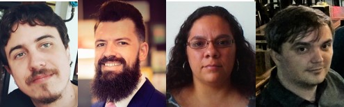
Four young B-MRS members are part of the team of invited editors of the latest issue of the Journal of Materials Research, a journal of the Materials Research Society (MRS). They are Bruno Vinícius Manzolli Rodrigues (Brazil University), Jorge Augusto de Moura Delezuk (IFPR), Mariana Amorim Fraga (Unifesp) and Rodrigo Sávio Pessoa (ITA).
From the left, Bruno Vinícius Manzolli Rodrigues (Universidade Brasil), Jorge Augusto de Moura Delezuk (IFPR), Mariana Amorim Fraga (Unifesp), and Rodrigo Sávio Pessoa (ITA).
The best undergraduate and graduate student contributions presented at the XVIII B-MRS Meeting (Balneário Camboriú, Brazil, September 22-26, 2019) will receive awards from B-MRS and ACS Publications, the scholarly publisher of the American Chemical Society.
To compete for awards, the author (student) must submit, by July 14, an extended abstract additional to the conventional abstract. Prizes will only be awarded for works presented by students at the symposia of the event, and only if the authors (students) are present at the ceremony, which will be held at the closing session of the event, on September 26.
B-MRS will award up to 46 contributions within the Bernhard Gross Award, that annually distinguishes the best student work from each symposium (up to 1 oral and 1 poster per symposium). To elect the winners, the committee will consider the quality of the extended abstract and presentation, as well as the scientific contribution of the work.
Among the winners of the Bernhard Gross Award, the top five oral and five best posters will receive a cash prize (US $ 500.00) and a certificate from ACS Publications.
The Periodic Table of Chemical Elements Underlies All of Our Modern Materials
Seminal work of Dmitri Mendeleev one hundred and fifty years ago revealed systematic interrelationships of all the chemical elements known and predicted at the time, and, remarkably, of those subsequently discovered.Those elements are the stuff of which everything and everyone we see is made. The phenomenal natural evolution of our world, including of life itself, assembles the necessary major and often crucial minor elemental ingredients required for Nature’s grand design. Mendeleev’s Periodic Table of the Chemical Elements and its legacy gave us the tools and understanding to invent and design well beyond what Nature has provided.
Whereas empirical uses of materials date to the Bronze and Iron Ages, our electronics, pharmaceuticals, and skyscrapers owe their existence to invention informed by knowledge of the properties of the elements and of the likely properties of myriad compounds and alloys that they form. Such research and invention continue apace in the laboratories of universities and companies with no end in sight. The community of materials researchers depends on, and fully participates in, this exciting progress. The International Union of Materials Research Societies (IUMRS) therefore enthusiastically endorses UNESCO’s declaration of 2019 as the “International Year of the Periodic Table of Chemical Elements (IYPT2019). See https://www.iypt2019.org.
According to IUMRS President Professor Y.F. HAN, “The thousands of researchers affiliated with our membership, who devote their careers to uncovering the next great innovation enabled by advanced materials, all rely on their early training which included Mendeleev’s Table and which emains invaluable in formulating the next new approach to solving problems and making new discoveries in the laboratory. It is therefore entirely appropriate for IUMRS to recognise this sesquicentennial anniversary on their behalf.”
IUMRS Head Office: Room 2112, No. 62 Zizhuyuan Road, Haidian, Beijing, China.
For more information about this topic, contact Dr. Fenfen Liang at +86 10 6872 2032, fax to 86-10-6872-2033, or email to liangff_cmrs@163.com.
Alternative contact: IUMRS Chief Advocacy Officer at cao@iumrs.net
Newsletter of the
Brazilian Materials
Research Society
Year 6, issue 5. June 7, 2019.
B-MRS News
– With more than 2,450 submitted abstracts, the XVIII B-MRS Meeting (Balneário Camboriú, 22 – 26 September 2019) sets a new record in the history of B-MRS annual meetings. Know more.
Featured Paper
A team of Brazilian researchers developed a method that allows studying the structure of nanomaterials locally and used it to understand the occurrence of disorder in the structure of nanocrystals. The method, which should help develop more efficient materials, is available to the community at LNNano. The study was reported in The Journal of Physical Chemistry Letters. Know more.
From Idea to Innovation
Using its own technology based on nanomaterials, Krilltech manufactures products that, without negative impacts on the environment, increase crop productivity and nutritional quality of food. The Brazilian startup plans to disseminate the benefits of its technology on planet Earth… and beyond. Learn more about Krilltech here.
Featured Scientist
We interviewed Norbert Koch, a professor at the Humboldt-Universität zu Berlin (Germany). Through fundamental research, the scientist made important contributions to the development of more efficient optoelectronic devices (such as LEDs and solar cells). At the B-MRS Meeting, he will talk about combining organic and inorganic materials into these devices. Know more.
News from B-MRS Members
– B-MRS founding member Edgar Zanotto (UFSCar) won the American Ceramic Society award for the best contribution to the study of phase equilibrium published in 2018.Know more.
XVIII B-MRS Meeting
(Balneário Camboriú, SC, Brazil, September 22 – 26, 2019)
More than 2.450 abstracts were submitted to XVIII B-MRS Meeting!
Upcoming dates for authors of works. Approval, modification, or rejection notifications will be sent by June 10. Abstracts that need modification must be corrected and resubmitted to the system by June 24. The authors of these abstracts will receive the final approval/rejection notices by June 30.
Awards for students. To apply for awards for undergraduate and graduate students (Bernhard Gross Award and ACS Publications Prizes), authors are required to submit an extended abstract by July 14. Learn morehere.
Venue. The meeting will be held in the delightful Balneário Camboriú at the Hotel Sibara Flat & Conventions, located in the center of the city, close to many hotels, restaurants and shops, and only 100 meters from the sea. More information, here.
Opening ceremony venue. The opening ceremony, the memorial lecture and the welcome cocktail will be held on September 22 (Sunday) at the Cristo Luz complex, one of the main tourist attractions in the city. There will be transportation to the venue, leaving the Hotel Sibara from 17:00 on. Know more about this place, here.
Memorial Lecture. The traditional Memorial Lecture Joaquim da Costa Ribeiro will be given by Professor Yvonne Primerano Mascarenhas (IFSC – USP).Know more about the speaker.
Event party. The party will be held in the lounge of the Green Valley, a prominent nightclub. Learn more about Green Valley here, aqui. The party will feature the striking Brothers band. Watch the Brothers,here.
Host city. Balneário Camboriú (SC) is an important tourist destination that offers urban and wild beaches, ecotourism and adventure sports, boat trips, bicycles and cable cars – all within a unique landscape that combines mountains, sea and skyscrapers. The visitor has access to many options of gastronomy, lodging and shopping, as well as the bustling nightlife that stands out in the Brazilian scenario.
Lodging, tickets, transfers etc. Check the hotel options and the official agency of the event,here.
Plenary lectures. Leading scientists from institutions in Germany, Italy, Spain and the United States will deliver plenary talks on cutting-edge issues at the event. There will also be a plenary session by the Brazilian scientist Antônio José Roque da Silva, director of CNPEM and the Sirius project (new Synchrotron Light Lab). Learn more about the plenary sessions,here.
Symposia. 23 symposia proposed by the international scientific community compose this edition of the event. See the symposia list,here.
Organization. The chair of the event is Professor Ivan Helmuth Bechtold (Physics Department of UFSC) and the co-chair is Professor Hugo Gallardo (Department of Chemistry of UFSC). The program committee is formed by professors Iêda dos Santos (UFPB), José Antônio Eiras (UFSCar), Marta Rosso Dotto (UFSC) and Mônica Cotta (Unicamp). Get to know all the organizers,here.
Exhibitors and sponsors. 38 companies have already confirmed their participation in the event. Those interested in sponsoring/support can contact Alexandre at the e-mail comercial@sbpmat.org.br.
Reading Tips
– Scientists are able to deposit inorganic epitaxial thin films (oriented with respect to the substrate) with simple and economic method (spin coating). This advance can massify these materials, required for electronic and optoelectronic applications (Science). Know more here.
– New 2D material: Scientists are able to make phosphorene nanoribbons, whose exceptional properties for energy and electronics applications have been predicted in more than 100 articles. The discovery happened accidentally (Nature). Know morehere.
– Organic semiconductors: Scientists reveal how nanotraps slow down conductivit in organic materials, and they show how to eliminate them (Nature Materials). Know morehere.
Opportunities
– Postdoctoral position on Perovskite materials and solar cells.Saiba mais.
Events
III Escola de Pesquisadores da USP. São Carlos, SP (Brazil). June 12 – 13, 2019. Site.
10th International Conference on Materials for Advanced Technologies (ICMAT 2019). Singapore. June 23 – 28, 2019. Site.
Webinar: Nanomaterials for Biomedical Applications. June 25, 2019. Site.
X Método Rietveld. Fortaleza, CE (Brazil). July 8 – 12, 2019. Site.
20th International Sol-Gel Conference. Saint Petersburg (Russia). August 25 – 30, 2019.Site.
21st Materials Research Society of Serbia Annual Conference (YUCOMAT 2019) and 11th IISS World Round Table Conference on Sintering (WRTCS 2019). Herceg Novi (Montenegro). September 2 – 6, 2019.Site.
XVIII B-MRS Meeting. Balneário Camboriú, SC (Brazil). September 22 – 26, 2019.Site.
XL CBRAVIC (Brazilian Congress on Vacuum Applications in Industry and Science). October, 7 – 11, 2019.Site.
XII Brazilian Symposium on Glass and Related Materials. Lavras, MG (Brazil). October, 22 – 25, 2019. Site.
19th Brazilian Workshop on Semiconductor Physics. Fortaleza, CE (Brazil). November 18 – 22, 2019.Site.
Follow us on social media
You can suggest news, opportunities, events or reading tips in the materials field to be covered by B-MRS Newsletter. Write to comunicacao@sbpmat.org.br.

 B-MRS Bulletin: Could you tell us briefly how and when you started and developed your interest in science/research? And your desire to become a scientist?
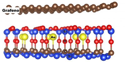
![This two-dimensional map series shows the concentrations of electrons and holes in the graphene sheet in the two graphene systems on the silicon carbide surface finished in Si [(a) and (c)] and terminated in C [(b) and ( d)]; in the presence of an aluminum monolayer [(a) and (b)] and the other containing a gold layer [(c) and (d)].](https://www.sbpmat.org.br/site/wp-content/uploads/2019/06/dopagem-grafeno.jpg)