|
||||||||||||||||||||||||||
|
||||||||||||||||||||||||||
|
|
||||||||||||||||||||||||||
|
||||||||||||||||||||||||||
|
[Paper: Decreasing Nanocrystal Structural Disorder by Ligand Exchange: An Experimental and Theoretical Analysis. Gabriel R. Schleder, Gustavo M. Azevedo, Içamira C. Nogueira, Querem H. F. Rebelo, Jefferson Bettini, Adalberto Fazzio, Edson R. Leite. J. Phys. Chem. Lett. 2019 10 1471-1476. https://doi.org/10.1021/acs.jpclett.9b00439]
Disclosing structural disorder in nanomaterials
It is known that it is very important to know and control the structure of a material (how its atoms are arranged in three-dimensional space) as it is largely responsible for the properties of the material and therefore for its applications. For example: regions of disorder in crystalline materials (whose atoms, ideally, are ordered in regular patterns) change some expected behaviors for these materials. Unfortunately, knowing the structure of some materials in detail can be a difficult task – particularly when it comes to nanomaterials.
Concentrating various skills and experimental and theoretical resources, a Brazilian team developed a method to establish the degree and location of disorder in the structure of crystalline and non-crystalline nanomaterials, interfaces and surfaces. The method, which is based on the combination of an experimental technique (transmission electron microscopy), a data analysis method (pair distribution function) and computational simulations, is already available to the scientific community at the Brazilian National Nanotechnology Laboratory (LNNano), and should help develop better performing materials.
In addition to developing the technique, the team applied it in the study of structural disorder in nanocrystals, which are basic elements of nanotechnology and are used for example, in solar cells and electronic devices. Although by definition they have ordered structures, these crystals of nanometric dimension can exhibit, in practice, regions with structural disorder.
In order to carry out the study, the scientists produced faceted nanocrystals of about 3.2 nm in diameter, formed by a core of zirconium dioxide (ZrO2), inorganic material, and a shell made up of organic substances known as ligands, whose atoms form chemical bonds with atoms that are on the surface of the inorganic nucleus. Ligands have the important role of stabilizing the nanocrystals, thus preventing them from aggregating.
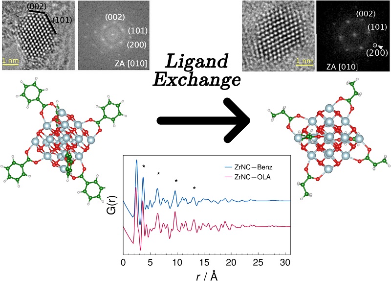
The team produced a first series of nanoparticles with ligands containing an aromatic ring and analyzed it using the developed method. The samples were then subjected to a process known as ligand exchange in which chemical reactions occur in the material in the presence of a solvent at a temperature above its boiling point. In these reactions, some connections break down and new connections occur. As a result of the ligand exchange, the team was able to produce nanoparticles with shells containing oleic acid, which were also analyzed using the developed method.

The scientists concluded that, unlike the ideal nanocrystal of zirconium dioxide, the two types of nanocrystals analyzed had a degree of structural disorder located on the surface of the nucleus. In addition, in the second group of nanoparticles, the disorder was significantly lower. The researchers interpreted this reduction as a result of the high temperature of the ligand exchange process, which altered the tensions of the network of atoms.
“In our work, we were able to directly assess the degree and location of disorder in the nanocrystals, which until then was not technically feasible,” says Gabriel Schleder, PhD candidate in the Graduate Program in Nanosciences and Advanced Materials of the Brazilian Federal University of the ABC (UFABC).
By better understanding structural disorder and its causes, the researchers were able to point out a way to control it. “Any property that significantly depends on surface-located structural disorder could be in principle controlled by this kind of ligand exchange process,” says Schleder. “Mechanical properties, photoluminescence, electronic transport and catalytic properties are some of them,” he adds.
The research was reported in a recently published article in The Journal of Physical Chemistry Letters (impact factor = 8,709).
Overcoming the challenge through collaborations
The initial idea of the study appeared in a meeting held at the end of 2017 at the National Center for Research in Energy and Materials (CNPEM), located in the city of Campinas, São Paulo. At the meeting, a group of reserachers discussed the implementation in Sirius (the next Brazilian synchrotron light source) of a technique that allows locally analyzing structural issues such as disorder and defects, called pair distribution function (PDF). The technique describes the distances between pairs of atoms by means of a mathematical function. To apply it, the specialist generally uses the results of X-ray diffraction measurements – an experimental technique that provides information about the structure of materials. However, in order to implement the analysis by PDF, the X-ray beam focused on the sample must be of very high energy – higher than that provided by the current Brazilian synchrotron light source.
During the meeting at CNPEM, Professor Gustavo de Medeiros Azevedo, researcher at the National Laboratory of Synchrotron Light (LNLS), and Professor Edson Leite, LNNano’s scientific director, decided to begin applying PDF using electron diffraction results, a specialty of LNNano’s researcher Jefferson Bettini. The electron beams would be generated by the transmission electron microscope (TEM) of LNNano. In fact, this instrument allows the control of the electron beam so that it focuses a small area of the sample, allowing the desired local analysis of the structure. Besides that, when switching from the “diffraction mode” to the “image mode”, the microscope would made possible to choose precisely the area of the sample to be analyzed.

The development team also involved professors Içamira Costa Nogueira, from the Federal University of Amazonas (UFAM) and Querem Hapuque Felix Rebelo, from the Federal University of the West of Pará (UFOPA), who contributed with the synthesis of nanocrystals that would be studied and with the development of the analysis methodology.
During the development of the technique, another challenge had to be faced. To interpret the PDF results, it would be necessary to have a simulation of an ideal nanocrystal – a nanocrystal model without structural disorganization that could be used as a reference.
New skills were then incorporated into the team, which was then joined by Professor Adalberto Fazzio, director general of LNNano and leader of a UFABC research group dedicated to computational techniques applied to materials, and his doctoral student Gabriel Schleder. Based on the Density Functional Theory (DFT), a computational modeling method in the field of Quantum Physics, the researchers were able to simulate the ideal nanocrystal that served as the analysis model.
“Something very positive we perceived is that the main results arose from the process of interaction, discussion and exchange of information mainly between theory/computational simulation and experiments. Without this, we certainly would not have good final conclusions,” says Schleder.


While a large part of humanity benefits from the advantages of solar cells, LEDs and other optoelectronic devices, some scientists are striving to find materials and structures that enable new developments in optoelectronic technologies.
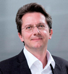
Norbert Koch (Professor at the Humboldt-Universität zu Berlin, and research group leader in that university and at the Helmholtz-Zentrum Berlin) belongs to the latter group of qualified people.
Prof. Koch studied technical physics at the Technische Universität Graz (Austria), where he also did his doctoral studies in solid-state physics. He spent two years as postdoc at Princeton University (USA). In 2003, he started setting up a research group at the Humboldt-Universität zu Berlin, where he was appointed as professor in 2009. His scientific production has more than 16,300 citations and his h-index is 66 (Google Scholar).
This scientist will be in September in Balneário Camboriú (Brazil), giving a plenary lecture at the XVIII B-MRS Meeting. In the talk, he will speak about very promising structures in the field of optoelectronics, which are based on a combination of organic and inorganic materials.
See our mini interview with Professor Norbert Koch.
B-MRS Newsletter: – We´d like to know more about your scientific work. Please choose one or two of your favorite contributions, briefly describe them, and share the references.
All modern optoelectronic devices are complex multilayer structures. To arrive at the desired function, e.g., light emission or energy conversion, with the highest possible efficiency, an optimized alignment of the electronic energy levels is key. For novel and emerging materials, such as organic and 2-dimensional semiconductors, this cannot be achieved readily because the fundamental underlying mechanisms, which govern the level alignment, are not properly understood. Consequently, my research is geared towards unraveling this understanding, and to devise means of optimizing interfacial energy levels. For instance, for a long time it was believed that the level alignment with organic semiconductors is substantially different from what was known for traditional inorganic semiconductors like silicon. The concerted effort of many groups worldwide has finally provided the insight that the established mechanisms do hold, but peculiarities of the organic compounds have to be considered appropriately. It turned out that the energy and density distribution of electronic states of the organic semiconductor critically determines the level alignment, at interfaces towards electrodes [Nat. Commun. 5, 4174 (2014)] and at semiconductor heterostructures [Sci. Adv. 1, e1501127 (2015)]. With this understanding at hand, device engineers can now minimize electrical losses at contacts and precisely tune the energy level offset at heterojunctions.
B-MRS Newsletter: – In your plenary talk at the B-MRS Meeting, you will talk about hybrid (organic / inorganic) structures for optoelectronics. Could you give examples of such structures and their present and/or future applications? Why this type of structure is relevant for developing optoelectronic devices?
The idea to combine inorganic and organic semiconductors is based on the notion to take advantage of the beneficial properties of each component while compensating their respective weaknesses. For instance, inorganic semiconductors typically exhibit high charge carrier mobility and organic ones stand out by very strong light-matter coupling. In a hybrid light emitting diode (LED), one can imagine to electrically pump the inorganic semiconductor at highest levels, and upon energy transfer the desired light is emitted by the organic semiconductor. This could result in LEDs with high brilliance at virtually any color that also feature ultrahigh modulation bandwidth.
For more information on this speaker and the plenary talk he will deliver at the XVIII B-MRS Meeting, click on the speaker’s photo and the title of the lecture here https://www.sbpmat.org.br/18encontro/#lectures.
Using nanotechnology to solve important human problems has for many years been a personal goal of Marcelo Oliveira Rodrigues, a professor at the University of Brasília (UnB) and a partner at Krilltech. One of these problems is undoubtedly the problem of food production. Data from the UN and FAO show that food demand will grow by more than 50% by 2050, while the expansion of areas available for agriculture will not keep pace with this growth.

Krilltech was launched on the market this year as the culmination of seven years of research, development and testing. The startup will soon be able to make its contribution, through nanotechnology, to a more productive and ecologically correct agriculture, which produces foods with better nutritional quality. “Our technology is a revolution in the modes of production and the way in which sustainable agriculture is done,” says Rodrigues.
In addition to some projects under development, the startup already has a portfolio of products, which includes a line adaptable to customer needs. The products can be applied to the soil or leaves of plants, or even in water, in the case of hydroponic crops. Krilltech products increase the photosynthesis rates of cultivated plants, make their water consumption more efficient and accelerate their metabolism (biostimulants). At the same time, they act as fertilizers to provide micro and macro nutrients that are necessary for plant growth (nitrogen, carbon, phosphorus, potassium, and others). “Our nanoproducts are multifunctional,” says Rodrigues. The startup also has a product line to incorporate mineral salts such as zinc and iron into grains and vegetables. “Producing potatoes, corn, lentils and chickpeas enriched with iron and zinc will contribute to resolving public health problems associated with the deficiency of essential minerals,” exemplifies the professor – researcher – entrepreneur.
Because they are based on nanotechnology, these biostimulants–fertilizers overcome the limitations of conventional technologies and are able to deliver much more nutrients to the crops. “Stabilizing in aqueous media all macro and micronutrients in a solution requires a high surface area and extremely hydrophilic material. Without nanotechnology this is an extremely difficult task,” explains Rodrigues.
According to him, Krilltech’s products do not affect the biota of soils and bodies of water, they do not accumulate in plant tissues (they are metabolized), and are not toxic to fungi, bacteria and animals. In order to guarantee the non-toxicity of its products, Krilltech counts on results of tests carried out with larvae, worms, fungi, bacteria, fish, several lineages of healthy and tumor cells and mice.
As for Krilltech’s production processes, they are of relatively low costs, partly due to the lean system adopted by the startup, based on leveling production according to demand and focusing on increasing efficiency and avoiding waste in production processes. “We work with sophisticated products, but production processes are efficient and we do not need imported equipment for our production,” says Rodrigues. In addition, Krilltech does not use toxic reagents in its processes and does not generate waste, says Rodrigues.
With these characteristics of its technology, production processes and products, Krilltech wants to gain a place in the growing biostimulant market, currently dominated by multinational companies headquartered mainly in Europe, North America and India. According to estimates reported by Krilltech, the demand for biostimulants will increase mainly in Asia and South America. It is estimated that this market will move around US$ 3.5 billion in 2022.
Emergence of the startup: a partnership between an university and a state-owned research corporation

“Transforming scientific research into technologies absorbed by the consumer market has always been a personal desire,” says Professor Rodrigues. So in 2012, shortly after joining UnB as an adjunct professor, he identified projects from his research group that had the potential to become innovations. By 2016, the group had developed a nanoformulation based on a high-cost drug, used in the Brazilian public system to treat fungal infections. “We were able to reduce the toxicity and cost of the drug by about 40 percent, but we were frustrated by the lack of resources to advance pre-clinical studies according to the Brazilian health regulatory agency standards,” says Rodrigues.
Also in 2016, the group began discussions with a unit of the Brazilian Agricultural Research Corporation, Embrapa. Initially, the goal was the development of plastics with special optical properties for use in protected cultivation (greenhouse and similar). “The conversations with Dr. Juscimar Silva (Embrapa) have evolved toward the development of our nanobiostimulants,” says Rodrigues.
The laboratory development of the technology was carried out at UnB, with the participation of undergraduate and graduate students, and with the support of the Brazilian government agencies FAP-DF, CNPq and Capes through scholarships and resources for consumables. “Public funding was essential for the early stages of development,” emphasizes Rodrigues. With support from Embrapa, the technology was tested on tomato, pepper and lettuce. “We are currently evaluating our products in the large monocultures of the country in partnership with national and multinational companies,” says the partner of Krilltech.
In 2018, the startup entered the pre-incubation program of the Technological Development Support Center (CDT) of UnB, which aims to assist in the development of the business model and the formalization of the future company.
Currently, Krilltech, together with UnB and Embrapa, is in the final stage of filing the patent application for the technology used in the products. “Krilltech has the exclusive right to exploit the technologies,” states Rodrigues.
Confident in the high performance of its products and agility in the development of innovations, Krilltech already has new partners and new projects. The startup has a partnership to enable hops culture in the center of Brasil. Also, Krilltech is testing its technology in microgravity conditions to contribute to farming projects outside the planet Earth (space farming). In addition, Rodrigues adds, a second startup will soon be created to explore nanobiopesticides of very low toxicity developed by the group.
See our brief interview with Rodrigues, PhD in Chemistry (2010) from the Brazilian Federal University of Pernambuco.
B-MRS Newsletter: What were the most important factors in enabling the creation and development of the startup?
Marcelo Oliveira Rodrigues: Undoubtedly, the support offered by UnB, the Brazilian Ministry of Science, Technology, Innovation and Communication and EMBRAPA in terms of technology protections, consulting and training were fundamental to the creation of Krilltech. However, I would like to emphasize that the crisis which Brazilian science has been subjected to and the difficulties of entering into cooperation agreements between the University and the private sector were two factors that contributed greatly to initiate this undertaking.
B-MRS Newsletter: What were the main difficulties the startup has faced thus far?
Marcelo Oliveira Rodrigues: Leaving the comfort zone implies difficulties that need to be overcome. Learning to undertake this endeavor required a cultural change in the way we planned and developed our projects; I think that was the great difficulty we have overcome.
B-MRS Newsletter: What, in your opinion, is the startup’s main contribution to society?
Marcelo Oliveira Rodrigues: Our technology contributes to reduce the environmental impact caused by the application of conventional fertilizers. For example, when fertilizer phosphorus and nitrogen are improperly leached to rivers, lakes and oceans, they can induce the formation of dead-zones, as the eutrophication process can induce excessive growth of algae that depletes water oxygen.
Unlike conventional nanomaterials (metal nanoparticles and metal oxides, polymer micelles, etc.), our technology enables the use of nanotechnology in agriculture. Krilltech has contributed to reformulating the fertilizer and phytostimulant industry, since our technology represents:
-The development of sustainable agriculture based on ecological agrochemicals;
-Contribute to eliminate and reduce the use of inputs and practices of hazardous agrochemicals (less hazardous chemical inputs);
-Mitigate environmental and human health risks due to non-toxicity of our products (design of safer chemicals);
-Elimination of the adverse impact of trophic transfer of conventional nanoparticles in the food chain;
-A disruptive paradigm needed for innovation in food production based on green nanomaterials.
B-MRS Newsletter: What is your goal/dream for the startup?
Marcelo Oliveira Rodrigues: We will have Krilltech units scattered around the world, we will see our technology contribute to sustainable development and we will contribute to reduce the impact of nutritional erosion and malnutrition.
B-MRS Newsletter: Leave a message to our newsletter readers and social network followers that assess the possibility of creating a startup.
Marcelo Oliveira Rodrigues: You should master the technology well, know the market and do not give up in the face of difficulties. The innovation environment in Brazil is unhealthy and standing out in these conditions increases the chances of success.

Professor Edgar Dutra Zanotto (DEMa – UFSCar), founding member of B-MRS, is one of two authors of the article selected by the American Ceramic Society to receive the Spriggs Phase Equilibrium Award of 2019. Entitled “Simple model for particle phase transformation kinetics,” the the award-winning article was published in the journal Acta Materialia in August 2018.
Since 2003, the award has distinguished the best contributions to the study of phase stability in ceramic-based systems among the works published in the calendar year prior to the award in the scientific literature (periodicals, books, bulletins, etc.).
The prize will be given on September 30 this year in Portland (USA) during the 121st ACerS Annual Meeting.
Paper: Reis, Raphael M. C. V. ; Zanotto, Edgar D. Simple model for particle phase transformation kinetics. ACTA MATERIALIA; v. 154, p. 228-236, AUG 1 2018
More than 2,450 abstracts were submitted to the XVIII B-MRS Meeting (Balneário Camboriú, Brazil, September 22 to 26). This number of abstracts sets a new record in the history of the annual meetings of B-MRS.
On June 10, authors of submitted papers will receive notification of acceptance, rejection, need for modification or transfer to another symposium. Authors will be able to submit corrected abstracts by June 24 and they will receive final notices by June 30.
The approved contributions will be presented in oral and poster sessions, within 23 thematic symposia, which cover a wide range of research topics in materials and their applications in segments such as health, energy, environmental remediation, electronics, photonics, defense , textile, aerospace and automotive, among others.
Words of the chairman (prof Ivan Bechtold)
“It is with great satisfaction that we have received this large number of submissions, showing that despite the financial difficulties and the lack of governmental stimulus, the scientific materials community is active and committed to carry out production of knowledge and training of human resources, which are so important for our country. At the same time, this expressive number of works increases our responsibility to organize an event according to the expectations, especially of students, who account for 63% of the registrations of the event. Our commitment is to make the event an environment conducive to the exchange of experiences and establishment of scientific cooperation. We count on the presence of all !! ”
Students awards
The best works presented by undergraduate or graduate students will receive awards at the end of the event. To apply for the awards, authors must submit an extended abstract in addition to the conventional abstract, by July 14. Prizes will only be awarded if the authors (students) are present at the closing ceremony on September 26.
The Bernhard Gross Award will be awarded to the best oral and best poster of each symposium. To elect the winners, the committee will consider the quality of the extended abstract and presentation, as well as the scientific contribution of the work.
Among the winners of the Bernhard Gross Award, the top five oral and five best posters will receive awards (cash and certificates) from ACS Publications, the renowned scientific publishing house of the American Chemical Society.
More information about the awards, and instructions and template for elaborating the extended abstract https://www.sbpmat.org.br/18encontro/#authors
Event website https://www.sbpmat.org.br/18concontro.
|
||||||||||||||||||||||||||||||
|
||||||||||||||||||||||||||||||
|
Many researchers are reporting problems with the submission system.
Therefore, on behalf of the Organizing Committee, the deadline for abstract submission will be extended until May 10th, 2019.
Don’t miss the opportunity of participating this important international scientific event on Materials Science and submit your Abstract for Oral or Poster Presentation.
[Paper: Gate-tunable non-volatile photomemory effect in MoS2 transistors. Andreij C Gadelha, Alisson R Cadore, Kenji Watanabe, Takashi Taniguchi, Ana M de Paula, Leandro M Malard, Rodrigo G Lacerda and Leonardo C Campos. 2D Materials, Volume 6, Number 2. DOI: 10.1088/2053-1583/ab0af1]

A scientific team from the Physics Department of the Brazilian Federal University of Minas Gerais (UFMG) developed a device based on ultrafine nanomaterials capable of recording and reading data, acting as computational memory. This memory, whose data storage mechanism originates based on optical phenomena – which is why it is called photo-memory – has shown to possess several of the characteristics currently desirable for memories: possibility of miniaturization, low power consumption, long data retention and relatively low cost.
The work opens up possibilities for developing efficient memories based on two-dimensional materials (those whose thickness is one or a few atoms) that could be used on lightweight and flexible platforms, such as wearable electronic devices. The research was reported in a recently published article in the scientific journal 2D Materials (impact factor 7,042).
“Our work consists of a scientific investigation with probable technological implications in the area of photo memories,” contextualizes Professor Leonardo Cristiano Campos (UFMG), corresponding author of the paper. “We developed a simple optoelectronic device, in which the simultaneous application of light and electrical charges modifies the electronic properties of molybdenum disulphide (MoS2), which is an ultrafine nanometric material,” he adds.

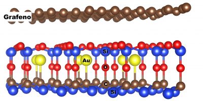
Initially, the doctoral students Andreij de Carvalho Gadelha and Alisson Cadore integrated a series of nanomaterials of few tens of nanometers in thickness, following the architecture of the field effect transistor (FET), which can be used as an electronic component of memories. The FET assembled at UFMG consists in essence of a layer of molybdenum disulfide placed on a flat crystal of hexagonal boron nitride, placed on a fine graphite substrate. Boron nitride was supplied by a research group from Japan, from the National Institute of Materials Science (NIMS).
The team then carried out a series of optoelectronic measures designed by the doctoral students Andreij and his supervisors (Professors Leonardo Campos and Rodrigo Gribel Lacerda), assisted by two opticians, Professors Leandro Malard Moreira and Ana Maria de Paula – all from the Physics Department of UFMG.
In general terms, the team simultaneously applied electrical voltage and laser radiation to FET. This combined action systematically changes the density of the free charges that travel through the molybdenum disulphide (semiconductor material), controlling the electrical conductivity of the material (process called photogating). The change persisted after the laser and tension were removed.
Thus, the scientific team generated in the material what is required to record data in digital electronics: two well-differentiated states that can be quickly detected and translated into the binary code such as zero (0) and one (1). Specifically, these are two states of conductivity of molybdenum disulphide: the one prior to the application of the laser light, called “off” or “0”, and the one subsequent to irradiation, called “on” or “1”, (this one characterized by the presence of the photocurrent).

In addition to revealing the ability of molybdenum disulphide FET to act as a photo-memory, the experiments and theoretical modeling performed at UFMG unveiled some very desirable characteristics in a memory: low power consumption (related to the ratio of “on” and “off”), and the ability to retain recorded data for long periods (the team estimated that up to 50% of a recorded data would remain saved after a decade).
The photo memory developed at UFMG demonstrated another interesting feature. By controlling the charge applied to FET, it is possible to modulate the conductivity states and generate a series of well-differentiated states (not only two).
“We believe that these memories can be applied in the long term,” says Professor Campos. To do this, says the scientist, it would be necessary to develop the large-scale production of nanomaterials, a challenge he estimates could be solved in a decade. In addition, it would require adapting the memory to the operation under environmental conditions, since the measurements carried out by the UFMG team were made in a vacuum. “We are developing encapsulation techniques that are likely to solve this issue,” says Campos.
The results reported in the 2D Materials article are part of Andreij Gadelha’s doctorate, who will defended his thesis on May 3. However, far from initially being chosen as a doctoral research subject, the molybdenum disulphide photo-memory effect was unveiled to the doctoral student and his advisor unexpectedly, as is often the case in the process of scientific discovery. “As if you’re looking at a specific point, but there’s that insight that turns your attention to the right path and you shout “EUREKA,” elucidates Professor Campos. Specifically, the doctoral student was attempting to annihilate certain effects that were undesirable in the context of the initial research, when he realized that these effects would enable an application in optical memories, and persuaded his advisor to change the focus of the work. “It is interesting to see that the undesirable effect has become our “golden-egg hen” leading to a turnaround in the direction of our research,” comments Campos.
The work was funded by the Brazilian federal agencies Capes, CNPq, the INCT of Nanocarbon and the Minas Gerais state agency Fapemig.
The board and directory of the Brazilian Materials Research Society (B-MRS) are publicly protesting against the budget cuts announced for the Ministry of Science, Technology, Innovations and Communications, which may render research and technological innovation in Brazil impossible. The Brazilian scientific system was developed over decades, based on the scientific community’s significant endeavor and on the support of different governments. The funding cuts of the Ministry in recent years have repeatedly subtracted resources for research and technological innovation, which further aggravates the country’s lack of competitiveness. These cuts pose a serious risk to Brazil’s performance in the coming years and decades. Even more serious is that, unlike other areas, the discontinuation of funding for science, technology and innovation in the country leads to the decline of researchers and disinterest of new generations of students, thus breaking the knowledge-building chain and hindering its resumption, due to the financial crisis.
The recent past has shown evidence that it is only through knowledge that the development and social well-being of a nation is achieved, and that countries have managed to escape economic crises through investment in science and technological innovation. There is no support that justifies cuts due to emergencies and urgencies brought on by a financial crisis. The amount of resources saved is insufficient to solve – or even significantly reduce – the country’s financial problems, given the already low investment in science and technology, lower than the criterion of any developed nations.
In a country with so many needs and so much inequality, as in Brazil, only technological development can improve the lives of our people, as demonstrated in recent decades. The efforts undertaken have led the country to a prominent position on the international scenario, which is now under threat, and to the rapid response of the scientific community to important economic and social issues, such as agribusiness and health. National development is only possible by means of a robust system of science, technology and innovation, with quality higher education and knowledge generation in different areas. In addition to the areas most directly related to technology, it is crucial that Brazil should develop research to identify the origins and propose solutions to our serious social problems.
If the relevance of education and knowledge generation for the country’s development is not recognized, in the long term the future of Brazil will be irreparably compromised.