The Department of Materials Physics and Mechanics of the Physics Institute of the University of São Paulo, Brazil, invites highly-motivated candidates to apply for two permanent positions, for a salary of R$ 10.049,62. Both openings are for Experimental or Theoretical Condensed-Matter Physicists, at the Assistant Professor level and is part of an initiative for further significant improvement of DFMT’s faculty.
The University of São Paulo has been consistently ranked among the top research institutions in Latin America. DFMT has proven academic excellence, and its faculty members are extremely active in many different topics such as New Materials, Nanoscience, Quantum Devices, Semiconductors, Biomolecular Physics, Organic Semiconductors, Complex Systems, Low-Temperatures Physics, and Magnetism.
New faculty members are expected to teach undergraduate and graduate courses, show research productivity commensurate with their experience, and a capacity to develop and sustain a research program that will result in peer-reviewed publications. They are also expected to advise students, provide service to the university, and sustain international collaborations. The application and the selection process can be done in Portuguese or entirely in English if the candidate does not speak Portuguese. We strongly encourage candidates from Brazil as well as from other countries to apply. The application forms and a description of the documentation necessary to apply can be found in the links Rules and Documentation (http://portal.if.usp.br/fmt/pt-br/node/1465 and http://portal.if.usp.br/fmt/pt-br/node/1467 ). We expect the presential interviews to take place late in the second semester of 2015 in order to start the appointment by March 2016.
More information about DFMT, its research activities and facilities can be found at
Brazilian Materials Research Society (SBPMat) newsletter
News update from Brazil for the Materials community
English edition. Year 2, issue 6.
SBPMat news: XIV Meeting – Rio de Janeiro, Sept 27 to Oct 1, 2015
Registrations: The early registration is open until July 31. The value of the registrations includes participation in the event, program book, welcoming reception, and daily coffee breaks. Learn more.
Meeting papers publication: authors of works presented in the meeting will have the possibility to submit papers to peer review for publication in IOP Materials journals. Know more.
Bernhard Gross award: Authors who are students can submit extended abstracts to compete for the award for best works (one oral and one poster) of each simposium. More info.
Hosting: A list of hotels is available, with special conditions for participants of the XIV SBPMat Meeting. Here.
Sponsors and exhibitors: 28 companies have already booked their place in the XIV SBPMat Meeting. Contact for exhibitors and other sponsors: rose@metallum.com.br.
The fourteenth edition of the annual meeting of the Brazilian MRS sets a new record in the history of these events, with 2,400 abstracts submitted to its 27 simposia and 2 workshops. Until July 10, the authors of the submitted papers receive their notes of acceptance, rejection or transfer to a different symposium. Know more.
XIV SBPMat Meeting: interviews with plenary speakers
Professor Ichiro Takeuchi, from the University of Maryland (USA), will talk in the SBPMat Meeting about the combinatorial approach in the field of Materials. This methodology, which substantially accelerates the rate of several research processes, has been helping Professor Takeuchi to discover a number of compounds and develop strategies to quickly determine the relation between composition, structure and property in many materials. In an interview with our newsletter, the scientist explains how the combinatorial research works in practice, and lists some of his main contributions to the field. He also discusses a topic of his plenary lecture: the “integrated materials engine”, which combines theory and high-throughput experiments in order to discover new materials. See the interview.
We also interviewed Professor Paul Ducheyne, from the University of Pennsylvania (USA). For about 4 decades, Ducheyne has dedicated himself to the study of biomaterials, field in which he is the author of hundreds of papers summing over 10,000 citations, besides 40 patents and books. In the interview, Ducheyne listed some of his most important contributions to the field, such as explaining how synthetic materials lead to tissue formation. In his plenary talk during the XIV SBPMat Meeting, Ducheyne will obviously address biomaterials; particularly bioactive ceramics with in situ functionalization and sol-gel materials used for the release of drugs and growth factors.See the interview.
Featured paper
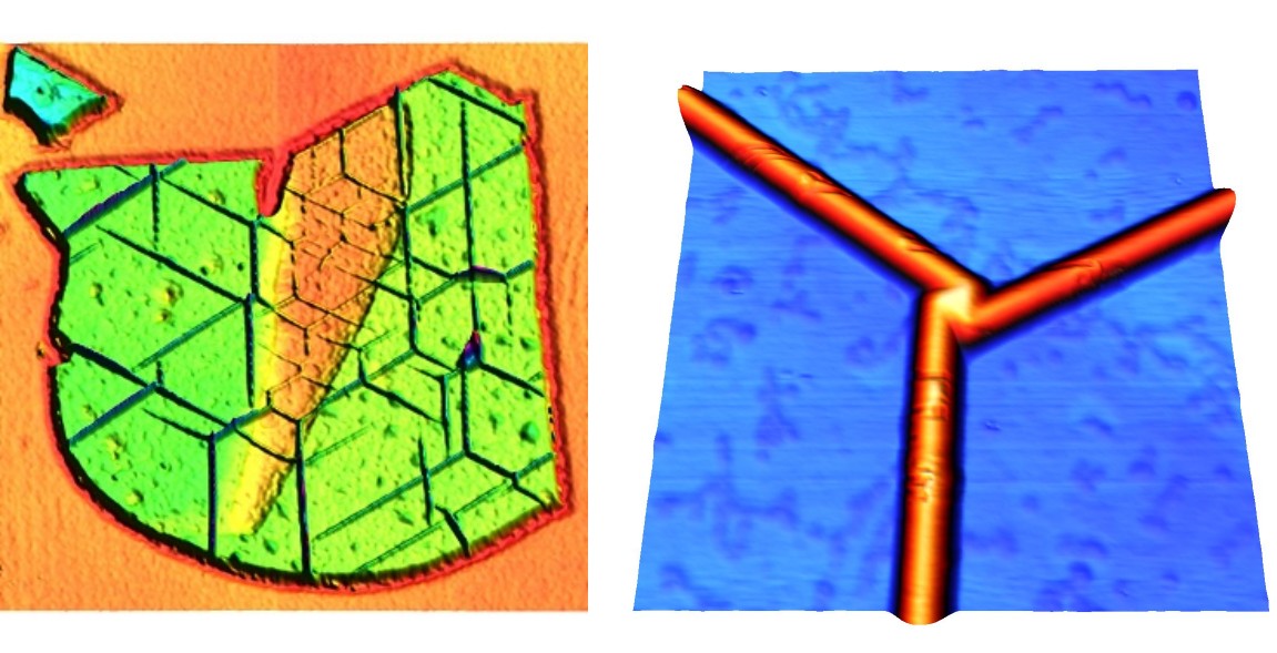
Analyzing AFM images of hexagonal boron nitride (a two-dimensional material), researchers from Brazil suspected that the nanometric folding pattern, which had formed as a result of annealing, followed a particular order. The scientists carried out a study involving experimental techniques, theory and simulations, and proved they were observing a phenomenon of strain organized in crystallographic directions. This property, new to two-dimensional materials, may come to be explored by straintronics. The paper has been recently published in Nano Research.See our story about the paper.
Reading tips
Books
“Refractory Castable Engineering”, a work with over 700 pages on refractory materials, authored by three Brazilian researchers, recently released by the Göller Verlag publisher (Germany). See the book flyer.
Scientific journalism stories based on highlighted papers
Innovating experimental set-up allows the study of friction between individual atoms – text and video (based on paper from Science). Here.
New, simple method to produce skyrmion bubbles enables more studies and applications to these magnetic particles (based on paper from Science). Here.
Nanothermometer with measuring range of over 300 degrees developed by team from Brazil and Germany (based on paper from ACS Nano). Here.
News from Brazilian National Institutes of Science and Technology (INCTs) and Research, Innovation and Dissemination Centers (CEPIDs)
Partnership between the Center for Development of Functional Materials (CDMF) and a company develops a system to prevent water waste by up to 30%. Here.
On the market: bottles double the shelf life of fresh milk, thanks to nanotechnology developed by a spin-off company of the CDMF. Here.
Proceedings of symposium N of the XIII SBPMat Meeting, co-organized by the National Institute of Surface Engineering, were published on Surface and Coatings Technology (Elsevier). Here.
See the winners of the competition of scientific images of surfaces organized by the National Institute of Surface Engineering. Here.
Events
Escola de Técnicas de Espalhamento de Raio-X (SAXS) e Neutrons (SANS) para Investigação Estrutural de Materiais e Sistemas Biológicos. Rio de Janeiro, RJ (Brazil). July, 6 to 10, 2015. Site.
XXVI Escola de Inverno de Física da UFMG. Belo Horizonte, MG (Brazil). July, 13 to 17, 2015. Site.
São Paulo School of Advanced Sciences (ESPCA) on Recent Developments in Synchrotron Radiation. Campinas, SP (Brazil). July, 13 to 24, 2015. Site.
Advanced School on Glasses and Glass-Ceramics (G&GC São Carlos). São Carlos, SP (Brazil). August, 1 to 9, 2015. Site.
III Escola de Química da UFRGS. Porto Alegre, RS (Brazil). August, 10 to 12, 2015. Site.
Primeira Conferência de Materiais Celulares (MATCEL 2015). Aveiro (Portugal). September, 7 to 8, 2015. Site.
XXII Reunião da Associação Brasileira de Cristalografia (ABCr) and I Meeting of the Latin America Crystallographic Association (LACA). São Paulo and Campinas, SP (Brazil). September, 9 to 11, 2015. Site.
Workshop em Ciências dos Materiais. São Carlos, SP (Brasil). 21 a 25 de setembro de 2015. Site.
XIV SBPMat Meeting. Rio de Janeiro, RJ (Brazil). September 27 to October 1, 2015. Site.
8th International Summit on Organic and Hybrid Solar Cells Stability (ISOS-8). Rio de Janeiro, RJ (Brazil). September 29 to October 1, 2015. Site.
13th International Conference on Plasma Based Ion Implantation & Deposition (PBII&D 2015). Buenos Aires (Argentina). October, 5 to 9, 2015. Site.
4th EPNOE International Polysaccharide Conference. Warsaw (Poland). October, 18 to 22, 2015. Site.
10th Ibero-American Workshop on Complex Fluids 2015. Florianópolis, SC (Brazil). October, 25 to 29, 2015. Site.
14th International Union of Materials Research Societies – International Conference on Advanced Materials (IUMRS-ICAM 2015). Jeju (Korea). October, 25 to 29, 2015. Site.
16th International Feofilov Symposium on spectroscopy of crystals doped with rare earth and transition metal ions. São Petersburgo (Rússia). 9 a 13 de novembro de 2015. Site.
43rd International Conference on Metallurgical Coatings and Thin Films (ICMCTF). San Diego (EUA). 25 a 29 de abril de 2016. Site.
To suggest news, opportunities, events, papers, interviewees or reading recommendations items for inclusion in our newsletter, write to comunicacao@sbpmat.org.br.
They are present in devices used in widely practiced medical procedures with the aim of treating or diagnosing health problems. They become part of the human body, temporarily or permanently, and interact, in a more or less active manner, with the biological system in which they are inserted. Obviously, we are talking about biomaterials. Examples of devices made of biomaterials are quite numerous. We can mention, among many others, stents that release drugs to achieve best results in the opening of arteries that are becoming blocked, and orthopedic implants that promote the regeneration of the bone tissue they are temporarily replacing.
Biomaterials is the subject of the XIV SBPMat Meeting´s plenary lecture that will be given by Paul Ducheyne. In the talk, Ducheyne will address, in particular, two kinds of biomaterials: bioactive ceramics with in situ functionalization, and sol-gel nanoporous materials that delivery drugs and other molecules.
Ducheyne is a Professor of Bioengineering and of Orthopaedic Surgery Research at the University of Pennsylvania (Penn), United States. He is also Director of the Center for Bioactive Materials and Tissue Engineering, a group of multidisciplinary research that brings together scientists from the Engineering, Dentistry and Medicine Departments at Penn. Besides, Ducheyne is a Special Guest Professor at the University of Leuven (KU Leuven), Belgium, where he obtained his MSc and PhD degrees in Materials Science and Engineering.
Paul Ducheyne is the author or editor of a number of books on biomaterials; in particular, he is editor in chief of “Comprehensive Biomaterials,” a 3,650 paged book divided into six volumes, published in 2011 by Elsevier publisher. Owner of a 58 H index, he has published about 330 scientific papers with more than 10,000 citations – of which some 2,600 belong to his 10 most cited articles. Ducheyne has also authored over 40 patents. In addition, from the 1980s on, he has organized several conferences and symposia in biomaterials.
In 1992, Ducheyne founded the company Orthovita, dedicated to products for treating injured bones and for controlling bleeding, and he was its CEO until 1999. In 2011, the company became part of Stryker Corporation, one of the leaders in the market of technology for medicine.
Paul Ducheyne was Secretary of the European Society for Biomaterials, and President of the US Society for Biomaterials and the International Society for Ceramics in Medicine. Among other awards and distinctions, in 2008 he won the C. William Hall Award of the Society for Biomaterials. Ducheyne was or is still part of the editorial boards of scientific journals in the fields of Biomaterials, Bioceramics, Bioengineering, Tissue Engineering, Orthopedics and Dentistry.
What follows is a mini-interview with this scientist.
SBPMat newsletter: – Could you briefly tell us what led you to devote to research on biomaterials?
Paul Ducheyne: – I was always attracted to medicine. In addition – when I graduated (in the seventies) – I foresaw the decline of the steel industry in the West, and I did not want to be caught into this. Therefore, my radical turning away from the then current materials science.
SBPMat newsletter: – How were you able to merge Materials Science and Biology in your scientific career?
Paul Ducheyne: – It is THE central theme in Biomaterials research.
SBPMat newsletter: – In your opinion, what are your most significant contributions in the field of biomaterials? Please explain them, very briefly, and share references from the resulting articles or books, or comment if these studies have produced patents, products, spin-off companies etc.
Paul Ducheyne: – Most people will know my mechanistic explanation for how synthetic materials (ceramics) stimulate cell function and lead to tissue formation. More recently, my using sol gel processed ceramics for controlled relase of a plethora of drugs and growth factors is also highly regarded. Lastly, I have published papers on a number of subjects (such as bone tissue ingrowth in porous materials, bone cement mechanical behavior, and titanium biocompatibility) which are highly cited.
The search for the materials that are most suitable for performing certain tasks maybe exists since the dawn of humanity. In this search, on the opposite end to the trial and error method, there is the combinatorial approach, which aims to increase the efficiency of the process of discovering or producing materials. This approach is based on the screening of large amounts of materials with compositions slightly different one another, using databases, rapid synthesis and characterization techniques, simulations, robots and other tools. The combinatorial approach has been applied to the pharmaceutical industry since the 1990s to identify new and useful compounds, and it also has its place in the field of Materials Science and Engineering.
Prof. Ichiro Takeuchi
During the XIV SBPMat Meeting, Professor Ichiro Takeuchi will give a plenary talk on the combinatorial approach to materials discovery – an issue that is part of his daily life. Takeuchi is a Professor of the Materials Science and Engineering Department at the University of Maryland, in the United States, since 1999. In this institution, he leads the Combinatorial Synthesis and Rapid Characterization Center and the Keck Lab for Combinatorial Nanosynthesis/ Multiscale Characterization. He is a Visiting Professor at the Tokyo University of Science since 2010. He is also member of the Executive Committee of the Forum on Industrial & Applied Physics from the American Physical Society (APS).
Takeuchi graduated with a Degree in Physics in 1987 at the California Institute of Technology (Caltech). For four years he worked in Japan at the microelectronics research laboratories of the NEC Corporation, to later return to the United States. In 1996, he earned his Ph.D. at the University of Maryland. Then, he went to the Lawrence Berkeley National Laboratory, where he stayed until 1999 as a postdoctoral researcher. In 2004, he was the chairman of the Gordon Conference on Combinatorial and High-throughput Materials Science. In 2009, he founded a company dedicated to the development of materials and systems for applications in the field of energy, the Maryland Energy and Sensor Technologies, LLC.
Ichiro Takeuchi was a Visiting Professor at universities in Japan and Germany. He has received awards and distinctions from the National Science Foundation (Career Award), the Office of Naval Research in the US (Young Investigator Program Award) and the University of Maryland, among other institutions. The scientist, whose H index is 40, according to Google Scholar, is the author of over 180 papers, with more than 5,900 citations, and a book on the combinatorial synthesis of materials.
What follows is a brief interview with this plenary speaker.
SBPMat newsletter: – Help us to visualize how the combinatorial research is performed. For instance, choose an example of a material created in your laboratories with this approach, and outline the “step-by-step”.
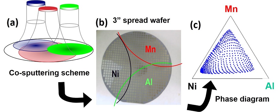
Synthesis of thin-film combinatorial library: in this example, co-sputtering (a) is used to generate large compositional variation across a 3” wafer (b); such a sample is called a composition spread wafer; the composition variation is mapped on to ternary compositional phase diagram using electron probe (c).
Ichiro Takeuchi: – We do thin film based combinatorial materials research. The goal is to carry out rapid screening of previously unexplored compositional landscape in order to discover new materials with enhanced physical properties. We make wafers or chips where there are large composition variations in deposited thin films. Sometimes the thin films are separated into different pads, and sometimes it is one continuous film with changing composition across the wafer. We want the variation to be as large and diverse as possible, so that we can map large compositional variation in a single experiment. We then take different characterization techniques to carry out rapid screening of various physical properties. For example, right now, we have a project to search for new permanent magnet materials. For this, we use techniques such as scanning SQUID or scanning magneto-optical Kerr effect measurements. These measurements can be used to map magnetic properties of all the compositions on a single wafer. These wafers and chips are called combinatorial libraries. We also do a lot of structural characterization. For this purpose, we often go to synchrotron beamlines. At such locations, because of the large beam flux, we are able to carry out x-ray diffraction of the entire wafer very quickly. Right now, we can scan 200-300 spots in 2 hours.
SBPMat newsletter: – In your opinion, what are your most significant contributions in the field of combinatorial materials science? Please explain them, very briefly, and share references from the resulting articles or books, or comment if these studies have produced patents, products, spin-off companies etc.
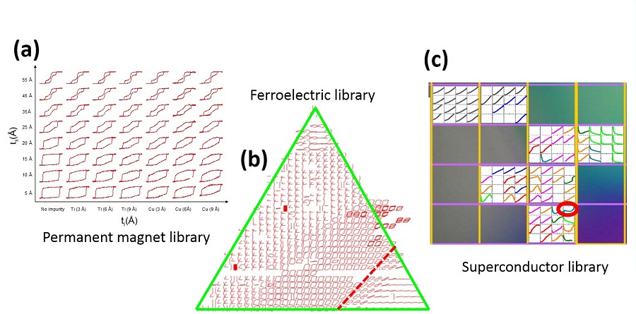
Examples of combinatorial libraries of functional materials and visualization of their data: (a) permanent magnet library for systematic investigation of exchange coupling showing magnetic hysteresis loops taken at each spot on the library (from Physical Review B75, 144429 (2007)); (b) ferroelectric library displaying ferroelectric hysteresis loops measured at each spot (from Journal of Materials Research 27, 2691 (2012)); (c) superconductor library with resistance – temperature curves mapped onto the positions where they were measured (from APL Materials 1, 042101 (2013)).
Ichiro Takeuchi: – Over the years, we have carried out combinatorial investigation on a variety of topics in the general field of functional materials. They include superconductors, shape memory alloys, magnetosrictive materials, ferroelectric and dielectric materials to name a few. In carrying out such experiments, we have had to develop and establish techniques to effectively implement the strategies. We have indeed discovered a number of new compounds. For instance, working together with theoretical colleagues, we have found shape memory alloys with long fatigue lives. I have patents on a number of low-loss dielectric materials as well as novel piezoelectric materials. Many groups are now doing follow-on work on a lead-free morphotropic phase boundary piezoelectric material we found a number of years ago. In addition to the materials that were discovered, we have established combinatorial strategies as a technique to rapidly delineate composition-structure-property relationships in different materials systems. We have recently published a comprehensive review article. It is: “Applications of high throughput (combinatorial) methodologies to electronic, magnetic, optical, and energy-related materials,” Journal of Applied Physiscs 113, 231101 (2013) by Martin L. Green, Ichiro Takeuchi, and Jason R. Hattrick-Simpers.
SBPMat newsletter: -If you wish, leave a message or an invitation to your plenary talk to the readers who will attend the XIV SBPMat Meeting.
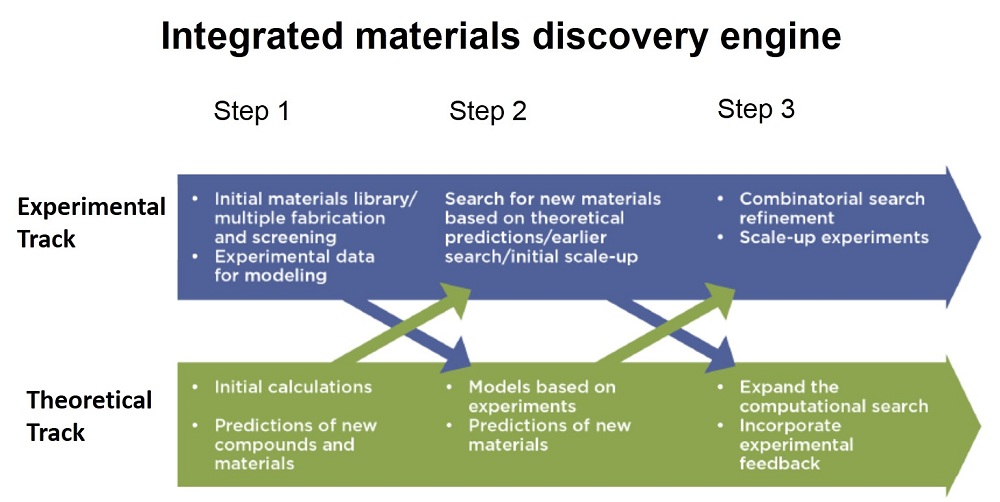
Ichiro Takeuchi: – The notion of search and discover is central to materials research. The combinatorial methodology is the natural counterpart to the concerted efforts in theoretical design of materials taking place around the world. By effectively coupling theory with high-throughput experimentation, we can really accelerate the rate at which new materials are discovered. I will present a mode of research we call “integrated materials engine” where theory and experiments are woven together and built on a flexible database and data management platform.
Integrated materials discovery engine: we propose coupling of high-throughput combinatorial materials exploration with theoretical investigation. Multiple feedback points between the two tracks ensure that we carry out accelerated exploration effectively.
With nearly 2400 abstracts submitted, the fourteenth edition of the annual meeting of the Brazilian Materials Research Society (SBPMat) sets a new record in the history of these events.
The term for submitting abstracts was closed on June 15. Until July 10, the authors of the submitted papers will receive their notes of acceptance, rejection or transfer to a different symposium. Abstracts written in Portuguese were refused.
Among the accepted papers, the ones whose authors are undergraduate or graduate students may compete for the Bernhard Gross Award, which will distinguish the best papers in each symposium (one oral presentation and one poster, at most). In order to compete, the authors, after being informed of their approval, must submit an extended abstract, in accordance with the instructions and the model displayed on the site of the event.
This year, the meeting counts with twenty-seven thematic symposia and two workshops, one on nanomanufacturing and the other on organic electronics in the industry, in addition to a symposium entirely organized by students enrolled in the SBPMat University Chapters (UCs).
The UC program at SBPMat was created in March 2014. It mainly aims to gather organized teams of graduate and undergraduate students from scientific and technological fields working in materials area, and officially link them to SBPMat. The activities to be carried out in such program intend to complement the academic development of these students, helping them to organize scientific and technological activities in materials fields, attend events held by the national and international scientific community, and establish exchanges with other UCs unities in the country and abroad.
The XIV SBPMat Meeting will be held in Rio de Janeiro, from September 27 to October 01st, 2015.
About the event
The SBPMat annual meeting is a traditional, international forum, dedicated to recent advances and perspectives on Materials Science and Technology. In the last editions, the event has gathered approximately 1,500 attendees, from the five regions of Brazil and dozens of others countries, for presenting and discussing scientific and technological studies in the field of Materials. The event also counts with plenary lectures, offered by internationally renowned researchers, and an exhibition of interest for the Materials community.
Paper: Crystal-oriented wrinkles with origami-type junctions in few-layer hexagonal boron nitride. Oliveira, Camilla K.; Gomes, Egleidson F. A.; Prado, Mariana C.; Alencar, Thonimar V.; Nascimento, Regiane; Malard, Leandro M.; Batista, Ronaldo J. C.; de Oliveira, Alan B.; Chacham, Helio; de Paula, Ana M.; Neves, Bernardo R. A. Nano Research. 2015, 8(5): 1680–1688. DOI: 10.1007/s12274-014-0665-y.
Camilla Oliveira at the atomic force microscope.
Camilla Oliveira was at the Federal University of Minas Gerais (UFMG), in Brazil, studying samples of hexagonal boron nitrite (hBN) with an atomic force microscope (AFM) within the framework of her doctoral studies in Physics, when one particular aspect of the control samples caught her attention and that of her advisor, Professor Bernardo Neves. After undergoing a heat treatment (annealing), the hBN had gained nanometric wrinkles, arranged in a geometric pattern that seemed to follow some sort of organization.
The researchers decided to study these wrinkles in more detail. They had an important question to answer: was there any relation between the arrangement of the wrinkles and the hBN crystal structure? In other words, did these wrinkles have a crystallographic orientation? Until that moment, there were no records in scientific literature of crystallographically-oriented wrinkles in two-dimensional materials, but this property could be useful.
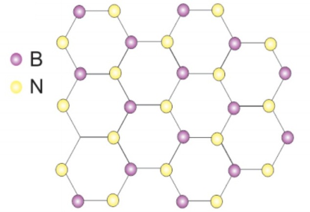
The two-dimensional hBN crystal lattice (1 atom high).
Camilla and her advisor joined other scientists from UFMG and the neighbor Federal University of Ouro Preto (UFOP) in order to carry out that research. The team produced samples composed of a few layers of hBN anchored on a silicon substrate, they heated them at 1,000 degrees Celsius and then cooled them. During this process, the silicon and the boron nitride displayed opposite strain behaviors. Due to the heating, the hBN contracts itself, while the silicon expands, shrinking the hBN. On the other hand, the cooling expands the hBN and shrinks the silicon, folding the boron nitride as origami paper.
After much experimental work using several techniques and approaches, and various simulations, the scientists were able to confirm that the wrinkles were forming in well-defined directions inside the crystal lattice. Analyzing the folding pattern in details, the scientists noticed the triangular-shaped joints by which the wrinkles (usually three of them) met.
AFM images of a 10nm thick hBN flake after the heat treatment, displaying a crystallographically-oriented pattern of wrinkles (left); details of a typical joint (right). The average height of the wrinkles is 10nm.
Detail: as proven by the Brazilian scientists, for the crystallographically-oriented folding patterns to be formed, the heat treatment must consist of rapid heating, followed by slow cooling (for example, citing the rates used in the research, 50 °C per minute to heat, and 8 °C per minute to cool). The wrinkles produced with faster cooling rates are arranged in a disorderly manner, with no crystallographic orientation.
The researchers have also concluded that this type of organized strain could happen, not only to hBN, but to other two-dimensional materials as well, such as graphene, and that it could lead to interesting applications in straintronics – the field of knowledge that studies and explores the capacity of some materials to have their properties deeply changed due to strain processes.
The results of the research were recently published on the scientific journal Nano Research.
“In my opinion, the main contribution of the paper is to present a property that may be shared by many two-dimensional materials: the organized strain, i.e., strain in well-defined crystallographic directions, of a material at the nanoscale”, says Professor Neves, who is the corresponding author of the paper.
The research was funded by the Brazilian agencies Capes, CNPq and Fapemig, and by INCT-Nanocarbono.