
|
|||||||||||||||||||||||||||
|
|||||||||||||||||||||||||||
|
|
|||||||||||||||||||||||||||
|
|||||||||||||||||||||||||||
|
![]() Symposium proposals for the XVII Brazilian MRS Meeting can be submitted from October 31st, 2017 to January 31st, 2018.
Symposium proposals for the XVII Brazilian MRS Meeting can be submitted from October 31st, 2017 to January 31st, 2018.
The meeting will take place at the Praiamar Natal Hotel & Convention Center, located at the Ponta Negra Beach, Natal, RN, from September 16th to 20th, 2018. The meeting chair is Prof. Antonio Eduardo Martinelli (Federal University of Rio Grande do Norte).
Proposals may be submitted by any PhD professor or researcher affiliated to a Higher Education and/or a Research Institution in Brazil or abroad, in any current field of Materials Science and Engineering. A submission form is available at http://sbpmat.org.br/proposed_symposium/.
The following data is required:
– Description of the symposium scope
– List of topics of interest
– Tentative list of invited speakers
– Names and contacts of symposium organizers
The organizing committee looks forward to having your contribution and participation at the 2018 B-MRS Meeting in Natal.
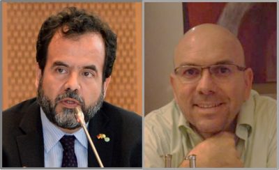
B-MRS President Osvaldo Novais de Oliveira Junior is the newest associate editor of ACS Applied Materials and Interfaces, an ACS Publications journal with an impact factor of 7,504. The full professor of IFSC – USP (Institute of Physics of São Carlos of the University of São Paulo) assumed this post in early September. At B-MRS, Oliveira Junior has been administrative director and counselor, and has been chairing the society since early 2016.
The Solar Energy journal (impact factor 4,018) also recently incorporated a member of B-MRS among its editors, Carlos Frederico de Oliveira Graeff, full professor and pro-rector of research at Unesp (Universidade Estadual Paulista Júlio de Mesquita Filho). Graeff was named associate editor in the area of Photovoltaics in this periodical of the publisher Elsevier. A member of B-MRS since its beginning, Graeff was scientific director of the society and served on the scientific committee of the B-MRS Newsletter.
Finally, Carlos José Leopoldo Constantino, also a professor at Unesp and a member of the B-MRS community, took over as Associate Editor in the Nanomaterials area of the Journal of Nanoscience and Nanotechnology (Impact Factor 1,483) from American Scientific Publishers.
|
||||||||||||||||||||||||||||
|
||||||||||||||||||||||||||||
|
![]() It is with great satisfaction that SBPMat announces the 17th edition of its annual event (XVII Meeting of SBPMat / B-MRS Meeting) to be held in the city of Natal (Rio Grande do Norte State), at the Convention Center of Hotel Praiamar, from September 16 to 20, 2018, under the coordination of Professor Antonio Eduardo Martinelli (Federal University of Rio Grande do Norte, UFRN).
It is with great satisfaction that SBPMat announces the 17th edition of its annual event (XVII Meeting of SBPMat / B-MRS Meeting) to be held in the city of Natal (Rio Grande do Norte State), at the Convention Center of Hotel Praiamar, from September 16 to 20, 2018, under the coordination of Professor Antonio Eduardo Martinelli (Federal University of Rio Grande do Norte, UFRN).
Save the date!
In the race to develop ever smaller and better performing chips, several technological limitations need to be overcome. Today, the bottlenecks to continue this trend lie mainly in techniques for manufacturing electronic circuits of less than 10 nanometers (nm). Among the techniques being improved to manufacture the next generation of chips, one of the most promising is extreme ultraviolet lithography (EUVL). This technology takes advantage of the very short wavelength of extreme ultraviolet radiation to pattern nanoscale circuits on the chip with the intermediation of the so-called “resists” – thin layers of radiation sensitive material that cover the chip substrate during nanofabrication.
At the XVI B-MRS Meeting, a plenary lecture will discuss an important contribution that the materials field can make to the next generation of chips: the development of suitable resists for the fabrication of electronic circuits of less than 10 nm through EUVL.
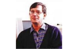
The subject will be presented by Kenneth E. Gonsalves, Distinguished Professor of the Indian Institute of Technology Mandi (IIT Mandi), a teaching and research institution created in 2009, where Gonsalves arrived in 2012 as a visiting professor.
Gonsalves obtained his BS in Chemistry from the University of Delhi (India) followed by an MS also in Chemistry from Boston College (USA) and a PhD from the University of Massachusetts at Amherst (USA) with a doctoral thesis on polymer synthesis. Then he performed a postdoctoral specialization on polymer ceramics at MIT (USA). From 2001 to 2014, Gonsalves was the Celanese Acetate Distinguished Professor of Polymer Materials at the University of North Carolina at Charlotte (USA).
Together with his research group at IIT and his collaborators from the United States, India, Brazil, Taiwan and Europe, Gonsalves carries out research and development on resists for advanced nanofabrication techniques, with support of major companies in the electronics segment, and on polymer scaffolds for tissue engineering.
Here follows a brief interview with the researcher.
B-MRS newsletter: – Tell us a little bit about your main scientific/ technological contributions up to the moment.
Kenneth Gonsalves: – My research has centered on polymers with an emphasis on synthesis of novel materials. For the last 20 years I have focused on resist technology for IC (integrated circuit) fab. This is a fascinating area as it has significant technological applications in the development of integrated circuits, solid state devices. In addition it can also be used successfully for cell and tissue engineering of scaffolds for biotechnologies.
B-MRS newsletter: – About the resists you are working on, what skills and expertise are needed to develop them, in your opinion? When this next generation of chips is expected to be available?
Kenneth Gonsalves: – Resist R&D is multifaceted and extremely complex. It requires extensive collaborations between chemists with organic, inorganic and polymer backgrounds. In addition, interaction with physicists and electrical/electronic engineers is essential. The next generation of chips at the 14 nm node are currently available. Sub 7 nm node technology is expected by 2018 onwards.
B-MRS newsletter: – Describe in the simplest and briefest possible way the process of EUVL, without forgetting to mention the role of resists.
Kenneth Gonsalves: – The EUV photons are generated by a plasma or synchrotron source operating at a wavelength of 13.5 nm. Through a series of special mirrors and a mask, the predesigned template for the IC fab is projected onto photosensitive materials such as polymers as well as inorganics. This is all conducted in vacuum, a challenge for the IC fab industry as it is a drastic change from current photolithography fab, which functions under ambient conditions. The extremely short EUV wavelength is a prerequisite for patterning features at the sub 20 nm scale. The challenges for resists that can meet the sub 7 nm node requirements are enormous. A new paradigm is paramount – hybrid resists, that are partially inorganic may provide solutions to patterning at these scales. Inorganic hardmasks are another alternative. The sensitivity of these photoresists has to be enhanced drastically in order to meet the mass volume production of chips. There are several other critical parameters that have to be met for a successful resist system. Again, this requires multidisciplinary, multi institutional, industry collaboration on a global scale.
——————
More information
On XVI B-MRS Meeting website, click on the photo of Kenneth Gonsalves and see his mini CV and the abstract of his plenary lecture: http://sbpmat.org.br/16encontro/home/
|
|||||||||||||||||||||||||||||||||||||
|
|||||||||||||||||||||||||||||||||||||||||
|
|||||||||||||||||||||||||||||||||||