
|
||||||||||||||||||||||
|
||||||||||||||||||||||
|
|
||||||||||||||||||||||
|
||||||||||||||||||||||
|
O artigo científico de autoria de membros da comunidade brasileira de pesquisa em Materiais em destaque neste mês é: Nanocatalysts for hydrogen production from borohydride hydrolysis: graphene-derived thin films with Ag- and Ni-based nanoparticles. Leandro Hostert, Eduardo G. C. Neiva, Aldo J. G. Zarbin, Elisa S. Orth. J. Mater. Chem. A, 2018,6, 22226-22233. DOI 10.1039/C8TA05834B.
Filmes de grafeno e níquel: melhores catalisadores para a produção de hidrogênio
Milhares de veículos movidos a gás hidrogênio já circulam em algumas regiões do mundo soltando apenas água pelo escapamento. Enquanto combustível ou fonte de energia, o hidrogênio é, de fato, uma opção extremamente limpa (não gera emissões nocivas) e eficiente (pode produzir mais energia do que qualquer outro combustível). Entretanto, o hidrogênio em forma pura não existe na natureza no planeta Terra. Ele precisa ser produzido, e a maior parte dos métodos de geração de hidrogênio conhecidos até o momento pecam tanto no aspecto econômico quanto no ecológico.
Uma alternativa a esses métodos foi recentemente apresentada por uma equipe de pesquisadores da Universidade Federal do Paraná (UFPR), ligados ao programa de pós-graduação em Química. Esses cientistas brasileiros propuseram um método limpo, eficiente, simples e de baixo custo para produzir hidrogênio. A equipe desenvolveu novos catalisadores (compostos que modificam a velocidade de uma reação química sem ser consumidos nela), feitos de grafeno e nanopartículas metálicas, que tornaram viável a produção de hidrogênio por meio da hidrólise de borohidreto – uma reação química ainda pouco utilizada na geração de hidrogênio apesar do enorme potencial que apresenta por ser limpa e muito simples.
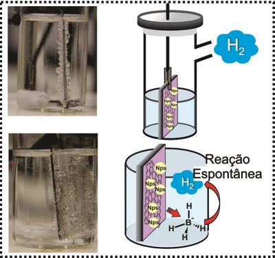
Nessa reação, que é realizada em temperatura ambiente, moléculas de borohidreto de sódio (NaBH4), reagem espontaneamente com moléculas de água gerando moléculas de hidrogênio (H2). O processo ocorre em apenas uma etapa, e é realizado com o auxílio de materiais catalisadores, que aceleram a velocidade da reação.
“O trabalho desenvolvido tem como principal contribuição a possibilidade de geração de H2 por meio de filmes finos de nanocompósitos de grafeno”, diz a professora Elisa Souza Orth, autora correspondente de um artigo sobre o trabalho, recentemente publicado no Journal of Materials Chemistry A (fator de impacto= 9,931). “Os nanocompósitos de materiais à base de carbono com nanopartículas metálicas têm mostrado muitas aplicações promissoras e mostramos que, para a hidrólise de borohidreto, menos explorada, eles também poderiam ser empregados com eficiência”, completa.
Dentre os filmes finos catalisadores produzidos pela equipe da UFPR, os que apresentaram melhor desempenho foram os de óxido de grafeno reduzido com nanopartículas de níquel (rGO/Ni). De fato, esse nanocompósito, produzido com um metal relativamente barato, o níquel, apresentou um desempenho superior ao da maior parte dos catalisadores já reportados na literatura científica, inclusive aqueles preparados com metais nobres, cujo custo é muito maior. Em linhas gerais, isso significa que pequenas quantidades de rGO/Ni (algumas dezenas de mg) geraram grandes volumes de hidrogênio (400 ml) em curtos prazos de tempo (5 horas).
Além disso, os filmes desenvolvidos pela equipe brasileira apresentaram mais uma característica importante para um catalisador: eles podem ser facilmente retirados do recipiente de reação, lavados e secados sem sofrer danos, possibilitando assim seu reuso. “Nesse trabalho, conseguimos reutilizar o mesmo nanocatalisador em 10 ciclos consecutivos, sem perder atividade”, conta a professora Orth.
Esses resultados foram possíveis graças à união das competências em fabricação de nanomateriais de carbono do Grupo de Química de Materiais, coordenado pelo professor Aldo José Gorgatti Zarbin com a expertise em processos de catálise do Grupo de Catálise e Cinética, liderado pela professora Orth. Esses dois grupos da UFPR têm um histórico de colaboração na aplicação de materiais de carbono; inicialmente, no estudo de pesticidas e, atualmente, no desenvolvimento de materiais multifuncionais com atividade catalítica extraordinária.
Além do desenvolvimento dos catalisadores e da sua aplicação na produção de hidrogênio, o trabalho publicado no Journal of Materials Chemistry A incluiu uma análise das diversas formas de se medir a atividade catalítica de um material. Os autores conseguiram uniformizar critérios e comparar diversos resultados obtidos no laboratório e encontrados na literatura científica. “Desenvolvemos um estudo cinético que complementa a discussão dessas reações complexas e pode ajudar a orientar para uma compreensão mais concisa da atividade catalítica”, explica Elisa Orth.
A pesquisa foi realizada dentro do doutorado em andamento de Leandro Hostert, orientado pela professora Orth, e contou com financiamento do CNPq, CAPES, Fundação Araucária, INCT Nanocarbono e L´Oréal–UNESCO-ABC por meio do Prêmio para Mulheres na Ciência (2015) e International Rising Talents (2016) recebidos por Elisa Orth.
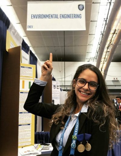
Quando era pequena, Juliana Davoglio Estradioto sonhava em ser cantora. Hoje, com 18 anos, os projetos dela são outros: seguirá a carreira científica. Uma carreira que, na verdade, já começou. Quando tinha 15 anos, Juliana se deparou pela primeira vez com um artigo científico e conheceu um laboratório de pesquisa. A partir desse momento, em apenas três anos, ela conquistou dezenas de prêmios em competições e feiras de ciências (locais, regionais, nacionais e internacionais) para estudantes do ensino médio. Entre essas distinções, talvez a mais glamorosa seja a que a levará, em dezembro deste ano, a passar uma semana na Suécia junto a outros 24 jovens pesquisadores do mundo para participar da cerimônia de entrega dos Prêmios Nobel 2019 e das comemorações com os laureados, além visitar instituições e empresas da Suécia e apresentar seu trabalho a estudantes suecos, entre outras atividades.
Juliana nasceu e cresceu em Osório (RS), um município de 40 mil habitantes, localizado a 100 km de Porto Alegre, rodeado por lagoas, serras e mar. Ali, em 2015, depois de concluir o ensino fundamental em uma escola pública estadual, ela ingressou ao Instituto Federal de Educação, Ciência e Tecnologia do Rio Grande do Sul (IFRS) – campus Osório, que tinha sido inaugurado cinco anos atrás, para cursar o Curso Técnico em Administração Integrado ao Ensino Médio. Criados por lei sancionada em 2008, os Institutos Federais (IFs) são instituições públicas e gratuitas, ligadas ao governo federal, que se especializam na oferta de educação profissional e tecnológica desde o ensino médio até a pós-graduação. Atividades de extensão e pesquisa fazem parte da proposta dos IFs para todos os níveis.
Já em seu primeiro ano no IFRS, Juliana se entusiasmou com um projeto de extensão voltado à comunidade de agricultores familiares da região, com viés social e ambiental, coordenado pela professora Flávia Santos Twardowski Pinto. Inicialmente como voluntária e depois como bolsista do IFRS, Juliana acabou participando de três projetos envolvendo pesquisa e desenvolvimento ao longo dos três anos do ensino médio, sempre orientada pela professora Twardowski.
O primeiro trabalho de Juliana resultou não apenas no desenvolvimento de um plástico biodegradável feito com resíduos agrícolas disponíveis na região (casca de maracujá), mas também na criação de uma aplicação para esse material: uma embalagem para mudas que não necessita ser retirada antes do plantio. Por esse trabalho, Juliana recebeu várias distinções, como o 4º lugar em Engenharia Ambiental na maior competição de ciências do mundo para estudantes do ensino médio, a Intel International Science and Engineering Fair (Intel ISEF), realizada em Los Angeles (EUA) em maio de 2017. Outro reconhecimento internacional importante foi a medalha de ouro obtida na Genius Olympiad, competição de projetos de ensino médio que abordam problemas ambientais e suas soluções, realizada em Oswego (EUA) em junho de 2018. Em nível nacional, a principal distinção recebida por Juliana pelo trabalho do plástico de maracujá foi o primeiro lugar da categoria Ensino Médio na 29 ª edição do Prêmio Jovem Cientista, outorgado pelo Conselho Nacional de Desenvolvimento Científico e Tecnológico (CNPq) e entidades parceiras. O prêmio foi entregue no Palácio do Planalto em dezembro no ano passado, com a presença do Presidente da República e várias outras autoridades governamentais.
No final do ano passado, quando Juliana concluiu o ensino médio no IFRS, ela já tinha uma opção concreta para a graduação: uma bolsa para estudar na University of Arizona (EUA), recebida como prêmio na Intel ISEF de 2018, da qual participou com um trabalho de desenvolvimento de materiais adsorventes a partir de resíduos agroindustriais para remoção de corantes em suspensão aquosa. Agora, ela tem, no mínimo, mais uma opção, pois foi aprovada no vestibular do curso de Engenharia Química da Universidade Federal do Rio Grande do Sul (UFRGS). Irá ficar na terra natal? Seja qual for a decisão, o histórico da moça faz pensar que saberá aproveitar as oportunidades.
Veja nossa entrevista com Juliana.
Boletim da SBPMat: – Você acabou de concluir o Ensino Médio Integrado ao Técnico em Administração. Quando você ingressou ao curso, pensava atuar na área de administração? O que a levou a participar de projetos de pesquisa científica?
Juliana Davoglio Estradioto: – Para ingressar no IFRS – campus Osório precisa fazer um processo seletivo, e já antes do processo eu precisava optar entre Administração e Informática. Foi muito difícil fazer essa decisão com 14 anos e acabei optando pela Administração. Nunca imaginei que fosse fazer pesquisa e muito menos que seria em temáticas tão diferentes do que eu via em sala de aula. Acho Administração uma área muito importante, mas não me vejo atuando na área; agora que sou Técnica em Administração, acabei me apaixonando pela pesquisa!
Assim que eu ingressei no curso me interessei muito por um projeto de extensão rural pois minha família é muito envolvida com a área de agronomia. A coordenadora era a professora Flávia e tinha que fazer um processo de seleção para entrar no projeto. Lembro da adolescente de 14 anos que estava morrendo de nervosismo, mas muito animada com a possibilidade de fazer algo diferente das aulas teóricas, uma vez que os IFs oferecem várias oportunidades. Logo em seguida já estava sendo orientada pela professora Flávia e admirando o trabalho que ela faz.
Boletim da SBPMat: – Complementando a pergunta anterior, como/quando surgiu e se desenvolveu em você a vontade de ser cientista? A participação nas amostras e competições foi importante nesse processo?
Juliana Davoglio Estradioto: – Quando eu era criança eu gostava de subir em árvores, observar insetos e ficar em contato com a natureza. Contudo, ao longo da infância aprendemos a ser mais contidos e nosso espírito investigativo diminui. Então eu nunca tive a vontade de ser cientista apesar de ser curiosa quando era criança, meu sonho de infância era ser cantora! E por isso digo que a ciência me escolheu e não o contrário, jamais imaginei que ia ser algo pelo qual eu ia ser tão apaixonada. Quando entrei no Instituto Federal, me envolvi em projetos e tive uma professora que realmente me incentivou a seguir nessa área. O contato com a ciência me ajudou a enfrentar um momento pessoal difícil, me fez querer ser uma pessoa melhor e mais determinada, além de persistente enquanto cientista. A participação em feiras de ciências foi mais importante na minha construção pessoal e auxiliou no desenvolvimento das minhas habilidades comunicativas e empatia, enquanto que o convívio no laboratório e a vontade de pesquisar me mostraram que eu quero fazer isso para o resto da vida.
Boletim da SBPMat: – Sobre o desenvolvimento do plástico biodegradável a partir de resíduos de maracujá, conte-nos brevemente o caminho percorrido, da ideia até a realização do material e da aplicação. Você consultou muitos artigos científicos? Trocou ideias com outros pesquisadores? Quais laboratórios usou?
Juliana Davoglio Estradioto: – O projeto do plástico biodegradável a partir da casca de maracujá surgiu a partir de um problema que eu observei na minha região a partir do projeto de extensão rural que eu participei no primeiro ano do ensino médio: que a indústria de processamento de frutos gera resíduos, sendo que no maracujá os resíduos correspondem a 70% do fruto. Eu queria trazer uma utilização para essa casca e a professora Flávia foi essencial no papel de me motivar e instigar a ir atrás de uma solução. Conversamos sobre ideias para o aproveitamento da casca e então eu descobri o que eram os artigos científicos. Foi um susto pois eu tinha 15 anos e não havia tido contato com artigos até então. Os artigos são um meio de comunicação mais acadêmico e eu tinha que descobrir muitas coisas antes de conseguir ler eles, pois minhas aulas no ensino médio eram básicas e as técnicas voltadas para a administração. Precisei aprender muito sobre Química e Biologia antes de conseguir entender os artigos, conversei com outros pesquisadores e muito consultei minha orientadora. No meio do desenvolvimento do projeto (quando estava tudo dando errado ahahahaha), descobrimos por coincidência que a primeira orientadora da professora Flávia estava trabalhando com filmes plásticos biodegradáveis, a professora Simone Hickmann Flôres. Assim foi possível fazer um intermédio e utilizar alguns laboratórios do Instituto de Ciência e Tecnologia de Alimentos da Universidade Federal do Rio Grande do Sul para fazer análises mais complexas, enquanto eu continuei fazendo a pesquisa no laboratório de panificação do IFRS – campus Osório (o único que tinha na época). Quando eu tive boas amostras de plástico, comecei a me questionar sobre a aplicação que poderia dar ao material. E foi aí que eu me lembrei justamente das visitas aos agricultores, em que eu tinha visto mudas envolvidas por um plástico preto (o polietileno de baixa densidade). Queria substituir esse material pelo meu plástico biodegradável e foi bem difícil até conseguir chegar em uma embalagem recipiente para mudas. O mais legal dessa aplicação é que a embalagem pode ser plantada junto com a muda, evitando a geração de lixo.
Boletim da SBPMat: – Em 2018 você começou a trabalhar em outro projeto ligado ao desenvolvimento de um material a partir de resíduos agrícolas, também coordenado pela professora Flávia. Poderia nos resumir do que trata esse trabalho e qual o status de desenvolvimento?
Juliana Davoglio Estradioto: – O projeto surgiu a partir da demanda de uma das maiores agroexportadoras da noz macadâmia aqui no Brasil, sendo que a noz está em ascensão no mercado mundial. O processamento do fruto para obter a noz que é comercializada gera um resíduo agroindustrial que é a casca de noz macadâmia. Essa casca normalmente é destinada a aterros sanitários ou para a combustão e produção de energia. O que eu queria fazer era uma aplicação biotecnológica, então minha hipótese foi se seria possível a utilização do resíduo agroindustrial da noz macadâmia na síntese de uma biomembrana polimérica. O projeto ainda está sendo desenvolvido e aprimorado, já consegui comprovar minha hipótese de forma positiva e estou buscando melhorar o aspecto das biomembranas.
Boletim da SBPMat: – A quais fatores e competências você atribui o sucesso que seus trabalhos tiveram em premiações nacionais e internacionais?
Juliana Davoglio Estradioto: – Acredito que minha vida seria completamente diferente se eu não tivesse estudado no Instituto Federal do Rio Grande do Sul, pois ele proporciona diversas oportunidades que infelizmente ainda não são ofertadas em outras escolas de ensino básico. Ter sido aluna do IF e orientada da professora Flávia fez com que minha visão sobre a educação e ciência mudassem, sou muito grata por entender o papel transformador que elas desempenharam na minha vida e em muitas outras realidades brasileiras.
Boletim da SBPMat: – A sua carreira em pesquisa científica começou com muitíssimo destaque. O que você pretende, do ponto de vista profissional, para os próximos anos ou para as próximas décadas da sua vida?
Juliana Davoglio Estradioto: – Pretendo continuar pesquisando nas áreas que sou apaixonada e ser uma cientista, gosto muito de ciências da natureza e acredito que nunca vá conseguir abandonar isso. Quero trabalhar com temáticas voltadas principalmente para a sustentabilidade, pois precisamos encontrar alternativas para o impacto que estamos causando em todos os ecossistemas. Contudo, além de ser uma pesquisadora, pretendo trabalhar com educação e divulgação científica.
Boletim da SBPMat: – Ao colocar seu nome no Google, a gente adivinha que a sua vida tem mudado bastante nos últimos tempos. São muitas entrevistas em todos os tipos de mídia, viagens, apresentações, premiações, formalidades, parabéns de políticos, conterrâneos e admiradores… Como você leva esta mudança?
Juliana Davoglio Estradioto: – É uma mudança muito positiva e representa muito para mim nesse momento, pois me sinto responsável pela divulgação de meninas que façam pesquisa no ensino médio. São atividades que me dão prazer e acredito que precisamos estimular outros jovens para que eles vejam a carreira científica como uma possibilidade e uma oportunidade.
|
||||||||||||||||
|
||||||||||||||||
|
O professor Sidney J. L. Ribeiro (IQ- UNESP – Campus de Araraquara), sócio da SBPMat, foi nomeado editor associado da revista Frontiers in Chemistry- Inorganic Chemistry.
A Frontiers in Chemistry, cujo fator de impacto é de 4,155, é um periódico da Frontiers – editora que publica artigos científicos revisados por pares na modalidade open access. Com apenas uma década de existência, a Frontiers ocupa atualmente o 4º lugar no ranking de editoras com mais citações por artigo.
O professor Ribeiro cumpria função de review editor na revista e agora passou a se desempenhar como associate editor. O cientista também é membro do corpo editorial das revistas Journal of Non-Crystalline Solids e Journal of Sol-Gel Science and Technology, ambas da editora Elsevier.

O programa University Chapters (UCs) da SBPMat inicia 2019 com um novo integrante, o UC da Universidade Federal de Pernambuco (UFPE). Com a criação desta unidade, o programa passa a contar com nove UCs distribuídos nas regiões sul, sudeste, nordeste e norte do país.
A equipe interdisciplinar do novo UC reúne 15 estudantes (três de graduação, cinco de mestrado e sete de doutorado) de cursos de Química, Ciências Biológicas e Ciência dos Materiais da UFPE. O tutor da unidade é o professor Petrus d´Amorim Santa Cruz Oliveira.
“O que nos motivou a criar nosso UC foi a necessidade de explorar o mundo da Ciência de Materiais, reinventando novos caminhos para ampliar e aproximar pessoas de todas as partes, desta forma diversificando e fortalecendo a nossa formação cada vez mais”, diz Karolyne Santos da Silva, presidente do UC. “Nossa expectativa maior é despertar o jovem para a ciência, mostrando que há possibilidades de ser inovador e de ter a oportunidade de vivenciar novas experiências com outros pesquisadores”, completa a doutoranda em Ciência de Materiais.
No contexto do programa UCs da SBPMat, a equipe planeja, inicialmente, realizar uma série de eventos: um curso de férias, o I Encontro de Ciência e Engenharia de Materiais de Pernambuco e workshops anuais.
Conheça o Programa UCs da SBPMat e as nove unidades que possui até o momento nos estados de Minas Gerais, Pará, Pernambuco, Piauí, Rio Grande do Sul e São Paulo: http://sbpmat.org.br/university-chapters/
|
||||||||||||||||||||
|
||||||||||||||||||||
|
Daniel Mario Ugarte nasceu em 23 de março de 1963 em Cosquín, uma pequena cidade nas serras da província de Córdoba (Argentina). Cresceu num ambiente familiar de muito estímulo à curiosidade, o aprendizado e a experimentação. Depois de cursar o ensino fundamental e médio nessa cidade, fez a graduação em Física na capital da província, na Universidad Nacional de Córdoba, a mais antiga do país vizinho (fundada em 1613). Após a graduação, fez um estágio em microscopia eletrônica de transmissão na Université Paris-Sud, na França, onde acabou ficando para realizar o doutorado em temas de nanociência (embora, naquele momento, o prefixo “nano” ainda não fosse amplamente utilizado). Ugarte obteve o diploma de doutor em Física em 1990. Mudou-se, então, para a Suíça, onde realizou um estágio de pós-doutorado que durou cerca de três anos na École Polytechnique Fédérale de Lausanne (EPFL). Ali continuou fazendo nanociência e nanotecnologia e obteve resultados de grande impacto acadêmico, notoriamente as “nanocebolas de fulereno”, que lhe renderam, aos 29 anos de idade, seu primeiro artigo na revista Nature, assinado apenas por ele e destacado na capa da edição. Esse paper, que hoje conta com mais de 2.000 citações, seria o primeiro de seis artigos publicados por Ugarte nas duas principais revistas científicas do mundo (a Science e a Nature), entre dezenas de publicações em periódicos científicos especializados, também de altíssimo impacto, como Nature Nanotechnology, Nano Letters, Physical Review Letters, entre outros.
Em 1993, por motivos pessoais, Ugarte foi morar no Brasil, e começou a trabalhar com a equipe que estava iniciando a construção do Laboratório Nacional de Luz Síncrotron (LNLS) no local atual, na cidade de Campinas (SP). Foi nesse contexto que ele pôde tornar realidade a sua ideia de construir um laboratório de microscopia eletrônica realmente aberto à toda a comunidade científica, sem esquecer os estudantes, que também cumprisse o papel de formar pesquisadores capazes de utilizar os equipamentos com habilidade. O Laboratório de Microscopia Eletrônica iniciou suas atividades em 1999, dirigido pelo cientista cordobés, e foi a semente do atual Laboratório Nacional de Nanotecnologia (LNNano). Entre 1994 e 1998, Ugarte atuou também como professor visitante na EPFL. Em 2004, o cientista deixou o LNLS para assumir o cargo de professor associado no Instituto de Física Gleb Wataghin (IFGW), da Universidade Estadual de Campinas (UNICAMP). Desde 2007, ele é professor titular dessa instituição. Além disso, de 2004 a 2007, o professor Ugarte coordenou uma rede de pesquisa em nanomateriais, a NANOMAT, que incluía 23 instituições e 150 pesquisadores.
Ao longo de sua carreira científica, Daniel Ugarte proferiu mais de 100 palestras convidadas em eventos científicos internacionais e recebeu vários prêmios prestigiosos por suas contribuições acadêmicas excepcionais, como o prêmio universitário da Fondation Latsis Internationale (Suíça, 1994), o John Simon Guggenheim Fellowship (EUA, 2002), o Prêmio Scopus Brasil da Elsevier e a CAPES (Brasil, 2008) e o prêmio de Física de The World Academy of Sciences, TWAS (Itália, 2018). Em 2012, Ugarte foi eleito membro da Academia Brasileira de Ciências (ABC). Além disso, vários estudantes orientados por ele receberam prêmios por suas teses de doutorado, outorgados pela Presidência da República (Prêmio Marechal do ar Casimiro Montenegro Filho), pela CAPES, pela Sociedade Brasileira de Física (SBF) e pelo IFGW – UNICAMP.
Daniel Ugarte é autor de mais de 100 artigos publicados em periódicos internacionais com revisão por pares. De acordo com o Google Scholar, sua produção acadêmica recebeu mais de 16.600 citações e seu índice h é de 43.
Veja a nossa entrevista com este sócio fundador da SBPMat e saiba mais sobre a sua história de vida, suas principais descobertas, suas críticas a algumas tendências no modo de se fazer ciência e sua mensagem aos pesquisadores mais jovens.
Boletim da SBPMat: – Gostaríamos de saber como/ por que você se tornou um cientista. Quando surgiu em você o desejo de ser cientista?
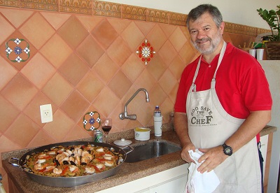
Daniel Ugarte: – Nasci na Argentina, com a informação genética típica daquele país: mãe de origem italiana, e pai de origem espanhola (basca, para ser preciso), mas tentando ser inglês (adoro rugby). Acho que o exemplo de curiosidade, trabalho e interesses variados de meus pais teve influência majoritária nas minhas escolhas. Nasci e cresci numa cidade no meio das montanhas/serras na Argentina (cidade de Cosquín, com aproximadamente 10.000 habitantes, na província de Córdoba). Minha mãe era professora do ensino fundamental e sempre tentava, com recursos financeiros muito escassos, obter livros para seguir estudando e melhorar suas aulas (naquela época não tinha internet); nós líamos em família esses novos textos de história, dinossauros etc. Meu pai, mesmo tendo frequentado a escola somente até os 12 anos, sempre foi muito curioso e ativo. Fazia de tudo como amador e autodidata; muito inquieto, era ator, pintor, músico, consertava de tudo, fazia chaves etc. A curiosidade e o espírito de criança ficaram sempre com ele: toda coisa nova, ele queria desmontar para ver como funcionava. Se tivesse que definir sua profissão, eu diria que ele fazia cartazes publicitários. Na oficina dele, todos os equipamentos foram construídos por ele mesmo. Naquela sala de bagunça constante, eu brincava furando ferros, soldando fios, cortando madeira, martelando coisas. Tínhamos poucos luxos, nenhum brinquedo caro, mas sempre havia livros, e eu fazia coisas muito incomuns (supervisionado por meus pais) aos olhos das outras crianças, tais como aeromodelos, rádios de galena, um telescópio etc. Com minha mãe, cozinhávamos sempre receitas novas (nhoques, bolos, alfajores, doces, etc.); aos 10 anos, todo domingo ao meio-dia, eu preparava o churrasco da família. Esses experimentos de química e calor foram muito instrutivos (e saborosos), sabores e aromas que tento ainda hoje reproduzir com precisão. Finalmente, para completar, tive a sorte de ter certa facilidade com Lógica e Matemática, a qual ficou em evidência quando fui para a escola. Tenho que agradecer muito aos professores de Ciência e Matemática que se esforçaram para manter minha motivação naquela cidadezinha e que eu pudesse crescer e fazer evoluir esse talento incipiente. Acho que com essa infância, o sonho de fazer ciência e trabalhar num laboratório (ou numa cozinha) fazendo descobertas e construir instrumentos maravilhosos é a consequência mais natural do mundo (devo esclarecer que fora do laboratório meu hobby principal é cozinhar).
Boletim da SBPMat: – Conte, brevemente, o que o levou a atuar no campo dos nanossistemas.
Daniel Ugarte: – Na verdade cheguei ao mundo “nano” pelas mãos da microscopia eletrônica. Na Universidad Nacional de Córdoba cursei Física, muito mais interessado no perfil experimental e no trabalho de laboratório utilizando as mãos. No curso, você deve fazer uma dissertação final para obter seu diploma. Entre as várias opções do Instituto de Física, preferi fazer um projeto associado à microscopia eletrônica de varredura e espectroscopia de raios X. Uma escolha pragmática visando ter mais opções de emprego após a minha graduação. Naquele momento, tive sorte, surgiu uma oportunidade de ir à França fazer um estágio em microscopia eletrônica de transmissão, e, após chegar lá (Laboratoire de Physique des Solides, Université Paris-Sud, Orsay), fui convidado a fazer uma tese de doutorado para estudar a excitação de plásmons de superfície em partículas pequenas (em inglês da época eram “small particles”, não “nanoparticles” como é hoje). O termo “nano” não existia ainda, e a “plasmônica” era somente uma curiosidade (hoje representa um dos temas de nanociência mais ativos). Uma vez concluída a minha tese, pude conseguir um pós-doutorado em Suíça, num dos primeiros institutos que concentrava suas pesquisas nas propriedades novas que surgiam ao diminuir o tamanho das partículas (Institut de Physique Experimentale, École Polytechnique Féderale de Lausanne). Resumindo, comecei nos embriões nano e sempre continuei estudando sistemas pequenos com técnicas de alta resolução espacial associadas à microscopia eletrônica de transmissão. A resolução atômica ou nanométrica desta técnica é imprescindível para a pesquisa básica ou tecnológica em nanossistemas, e os caros microscópios se tornaram símbolos para exibir a riqueza de cada programa “nano”.
Boletim da SBPMat: – Quais são, na sua própria avaliação, as suas principais contribuições científicas/ tecnológicas à área de Materiais e por que as considera mais relevantes?
Daniel Ugarte: – As nanoestruturas de carbono (fulerenos, nanotubos, grafeno) representam um exemplo típico de nanomateriais com propriedades novas. Considerando datas, os fulerenos foram descobertos em 1986, o sólido de fulerenos em 1990, os nanotubos em 1991. Trabalhando na Suíça em 1992, observei acidentalmente que, irradiando materiais de carbono com o feixe de elétrons de um microscópio eletrônico de transmissão, tudo se transformava em “cebolas de fulereno” (esferas concêntricas de grafite, como uma boneca russa). Este experimento gerou um novo membro para a recentemente descoberta família dos fulerenos, e o trabalho teve uma incrível repercussão a nível mundial. No entanto, o interessante foi que esse não era meu projeto de pós-doutorado, o qual era uma pesquisa mais focada no estudo da difração eletrônica de nanopartículas metálicas. Em Lausanne tínhamos um laboratório de microscopia completo e com todos os equipamentos de fronteira. E notei que ninguém os usava de noite; então, decidir ir lá brincar… fazer experimentos exploratórios, inocentes, alternativos e, sem querer, apareceram as cebolas…. Mas quando falei pela primeira vez dos resultados ninguém acreditou; um revisor da prestigiosa revista Physical Review Letters falou que meus dados eram tão ridículos como os da fusão fria (tema altamente controverso naquele momento); foi um insulto do pior nível. Mas eu continuei defendendo meu trabalho, eu obtinha os mesmos resultados uma e outra vez, e era a verdade. Eu continuei apresentando o resultado nos congressos; sobrevivi a muitos comentários violentos e humilhantes. Para fazer coisas um pouco fora do paradigma é preciso ter “couro duro”. Finalmente, com o apoio inesperado e espontâneo de Sir Harry Kroto (que recebeu o Prêmio Nobel de Química em 1996), que não me conhecia nem nunca tinha falado comigo, meu artigo foi publicado na revista Nature. Eu tinha menos de 30 anos, era muito inocente, e fiquei muito surpreso com o enorme interesse da mídia, pois dava reportagens para muitos países, entre eles Japão, Alemanha etc. Sentia como se o mundo estivesse caindo sobre a minha cabeça. Com experimentos “naifs” (despretensiosos) e fora de contexto, feitos à noite, com instrumentos avançados, eu tinha criado opções de trabalho que batiam na minha porta. Porém, nesse momento, para surpresa de meus colegas franceses e suíços, tomo um caminho alternativo, e em 1993 opto por vir viver no Brasil por razões pessoais e familiares.
Poucos anos depois, estávamos, numa tarde de sábado de 1995, no laboratório em Lausanne, fazendo propostas de ideias ousadas (“brain storming”) com meu amigo Walt de Heer (um cientista incrível considerando profundidade e criatividade). Decidimos testar uma que surgiu lá na hora: utilizar nanotubos de carbono (a ponta é bem fininha mesmo) para produzir uma fonte de elétrons. Juntamos uma prensa hidráulica, fita de teflon de tipo encanador, grades de microscopia, mica velha, umas coisas do laboratório (câmara de vácuo, osciloscópio etc.) e montamos uma coisa horrível, suja, grotesca, completamente improvisada e… funcionou!!!. O resultado foi publicado na revista Science. Esse experimento criou uma nova área de pesquisa aplicada para os nanotubos de carbono que vários laboratórios industriais tentaram explorar; até hoje é uma área ativa de pesquisa. De novo, no meu caminho, outra proposta experimental inocente, mas criativa e descontraída (neste caso o resultado não foi acidental, mas planejado), que captou o interesse da comunidade tecnológica internacional.
No meu grupo no Brasil, decidi investir numa nova linha de pesquisa baseada num experimento irreverente proposto na Espanha por um pesquisador chamado Costa-Kramer (Nanowire formation in macroscopic metallic contacts: quantum mechanical conductance tapping a table top, Surf. Sci. 1995). Se juntarmos dois pedacinhos de ouro e depois os separarmos, no fim se forma um fio muito fino (como com chiclete) que pode até ter um átomo de diâmetro. Medindo a corrente elétrica que atravessa esse fio durante a elongação, podemos estudar efeitos quânticos na condução elétrica por nanoestruturas. Em Campinas, meu estudante Varlei Rodrigues (que depois recebera o Premio SBF de Melhor tese de Doutorado em Física em 2003) construiu um instrumento especificamente desenhado para realizar esse estudo com alta precisão em condições de ultra alto vácuo (UHV). Posteriormente pudemos fazer imagens de microscopia eletrônica do arranjo atômico dos fios gerados por elongação mecânica e também cálculos teóricos em colaboração com o grupo de Douglas Galvão. A partir dessas informações pudemos compreender em detalhe as nossas medidas experimentais; a partir desses resultados fui convidado a proferir quase uma centena de palestras em conferencias internacionais. Considero que esses resultados foram muito importantes do ponto de vista brasileiro, pois toda a pesquisa foi integralmente feita no país: as ideias, os experimentos avançados, a construção de instrumentação científica especifica, os cálculos teóricos e a compreensão. Além do impacto científico, a pesquisa sobre nanofios metálicos representa uma realização importante, pois nos permitiu mostrar, pelo exemplo, que estudos de nanociência experimental competitiva, podem, sim, ser feitos no país, combinando trabalho com originalidade e um certo grau de risco.
Falar de resultados alimenta nosso ego (o pequeno argentininho que todos levamos dentro…); outro aspecto de nossa contribuição para a sociedade vem quando nosso esforço é dedicado ao crescimento da comunidade, em particular para elevar o nível da ciência do país. Neste sentido, gostaria de lembrar um dos trabalhos mais reconfortantes de minha carreira: a idealização e criação de um laboratório multiusuário de microscopia eletrônica em Campinas. Esse projeto contou com o apoio constante e incondicional dos diretores do LNLS na época (Cylon da Silva, Aldo Craievich e Ricardo Rodrigues). Finalmente, os microscópios foram adquiridos com recursos (muitos recursos!!!) da Fundação de Amparo à Pesquisa do Estado de São Paulo (FAPESP). Desde a ideia inicial, trabalhei para que o laboratório fosse aberto e disponível aos pesquisadores brasileiros (não nas intenções, mas na realidade) e que também tivesse formação de recursos humanos como um foco de suas atividades. Contrariando a opinião geral da comunidade, no laboratório de microscopia todas as observações eram realizadas pelos próprios alunos de graduação ou pós-graduação envolvidos nos projetos, após um processo de treinamento. Muitos estudantes aprenderam a trabalhar, e os instrumentos nem quebravam, mas tivemos que nos dar o tempo de ensinar os pesquisadores interessados. Este modo de operação tinha como alvo evitar o sistema feudal (“senhor dono” de instrumentos) ou aplicação de sicofantismo. Fiquei nesse laboratório até 2009. Esse laboratório cresceu e se transformou no que hoje é chamado Laboratório Nacional de Nanotecnologia (LNNano).
Boletim da SBPMat: – Você possui uma quantidade fora do comum de artigos publicados em revistas de altíssimo impacto (Science, Nature, PRL …), principalmente no contexto de países em desenvolvimento. A quais fatores e competências você atribui esta característica da sua produção científica?
Daniel Ugarte: – Na pergunta anterior tentei dar vários exemplos de alguns momentos importantes de minha atividade científica. Tem contribuição do volume de trabalho, muito estudo, bem como a coragem de assumir riscos para fazer experimentos ousados e originais. Mas tem uma coisa que sempre tento ensinar aos meus estudantes: se nós fizermos um projeto, ele deve descascar um abacaxi e trazer uma contribuição relevante (se der certo…). Se alguma publicação for gerada, tem que contribuir com conhecimento novo, não de mentirinha, mas de verdade. Não vamos escolher somente temas de pesquisa que gerem resultado rápido; provavelmente o nosso estudo vai demorar, teremos que entender e aprofundar em muita coisa nova. Até podemos precisar desenvolver ferramentas/instrumentos/
Outro aspecto, fora o risco ou ousadia, é a qualidade; todo estudante ou colega que trabalhou comigo sabe que sempre fazemos o melhor possível, não tem “mais ou menos”. Só o melhor é aceito, ou, então, tem que fazer o experimento de novo até obter a mais alta qualidade. Alguns alunos me detestam, mas recentemente um antigo aluno da UNICAMP (hoje professor nos Estados Unidos) publicou um artigo na revista Nature, e me enviou uma mensagem agradecendo, pois hoje ele dá um enorme valor àquilo que aprendeu sobre puxar seus limites, nessa convivência comigo. Puxar a qualidade total do conteúdo do estudo, nos experimentos – que são a base em nosso grupo -, no estudo teórico, na interpretação, na modelagem etc. Como em todas as profissões, nós construímos nossa reputação ao longo dos anos, e ela pode ser prestigiosa ou não. Sempre foi um orgulho para meu grupo que nossos colegas e competidores recebem nossos trabalhos com atenção, acreditando que fizemos nosso melhor para cada resultado publicado (mas nem sempre concordam com nossas conclusões/interpretações… como todo mundo temos muitos artigos rejeitados).
Quando formei parte do comitê que analisa projetos no CNPq, fiquei surpreso pelo número de pesquisadores brasileiros que publicam mais de, digamos, 50 artigos por ano, mesmo alguns tendo altos cargos administrativos ou gestão em instituições de ensino ou pesquisa do Brasil (funções que requerem esforço concentrado as 24 horas do dia). Considerando minha capacidade de fazer pesquisa, acho totalmente impossível pensar em fazer quase uma publicação por semana!!! E isso se ficasse no laboratório o dia todo com os estudantes. Neste ponto gostaria de retornar ao conceito de qualidade, considerando o número e a contribuição científica de artigos gerados por um grupo ou pesquisador. Podemos assumir que segue uma distribuição estatística com forma de gaussiana descrita por dois parâmetros com uma média e uma largura (notas de 1 a 10). Conheço pesquisadores com produção um pouco incoerente, capazes de fazer o melhor (trabalho nota 10), e ao mesmo tempo, o pior (alguns trabalhos merecem nota muito baixa, digamos 1-2). Seja um grupo hipotético no qual a média de contribuição ao conhecimento por publicação é boa/muito boa (média 6 ou 7), e são geradas várias dezenas de publicações. Estatisticamente você deve publicar, entre essas dezenas, algum artigo com conteúdo de alta qualidade (lado superior da distribuição e longe da média) que obterá reconhecimento na comunidade (eventualmente, com sorte, publicado numa revista de alto impacto). Mas se você faz 100 publicações por ano e nenhuma atinge uma certa relevância na sua área de atuação, o nosso modelo estatístico simples indica que a contribuição média de seus trabalhos deve ser moderada. Além disso, também pode ser moderada a largura da distribuição; nesta situação, sua produção/trabalho é coerente, numa faixa estreita de nível de qualidade. As causas podem ser variadas; em alguns casos, a justificativa/explicação não precisa de longos discursos, é razoável associar contribuição moderada a, por exemplo, a juventude do pesquisador, infraestrutura deficiente ou financiamento limitado. O ponto crítico é quando o problema está na raiz, e as causas da qualidade moderada estão associadas à pesquisa dirigida para perguntas/alvos científicos/técnicos de menor importância e baixo risco. O que esperar de um ambiente, onde tanto as agências financiadoras como também os próprios pesquisadores (não é só culpa das agências) aceitam que essa séria deficiência pode ser compensada plenamente pelo número de publicações? O resultado será que os números crescerão, mas o impacto diminuirá.
Talvez eu seja irresponsável, teimoso (as raízes bascas ajudam), mas meu trabalho ao longo dos anos seguiu certos padrões. Prefiro fazer um prato de alta gastronomia (as vezes meio queimado), do que fazer centenas de pratos de arroz e feijão. Prefiro fazer menos coisas e não ter numerosas publicações irrelevantes envolvendo trabalho que não incluiu risco nenhum (também tenho desses trabalhos), e assim ter tempo de me atualizar, me desafiar, estudar e ver coisas fora de meu principal interesse. Assim tenho a oportunidade para novas ideias, inocentes, irresponsáveis, que com sorte vão dar certo. É importante, primeiro, ter claro que coisa nova/diferente vamos fazer em nossa pesquisa; se não tem nada novo/arriscado, como vai ser a contribuição à geração de conhecimento? Na realidade, essa linha de pensamento não é muito popular se olhamos em detalhe a maior parte dos projetos financiados na comunidade brasileira (no entanto, muitos discursos e planejamentos a definem como essencial). Ao contrario, a viabilidade é muitas vezes mais importante que a relevância e a originalidade. Nem falar de outros temas que dificultam o aumento da relevância da pesquisa em nanociência no Brasil, tais como física experimental, instrumentação científica, multidisciplinaridade, onde o contraste entre discurso e realidade dá enorme tristeza. Como na gastronomia, prefiro o “slow food”, um bom prato, bom vinho e tempo para desfrutar. Devemos nos rebelar contra a “fast science” (projetos short-term), pois isso está levando à uma ciência superficial (shallow-knowledge).
É triste ver a evolução do Brasil, os números crescem, o impacto diminui… Muitos podem ver positivamente a publicação em revistas de alto impacto, mas nem todos concordam. Vou dar um exemplo. Decidi estudar alguns temas novos onde considero que existem oportunidades de coisas muito originais e interessantes. Para fazer perguntas mais profundas, é preciso entender. Aprender toma tempo… Assim, meu relatório de atividades teve problemas para ser aprovado por baixa produtividade: não atingi a média. Nunca tive muita diplomacia nem habilidades políticas, portanto, juntando toda minha revolta, e sendo argentino e basco ao mesmo tempo, pergunto-me: será que sou terrivelmente ineficiente e devo me aposentar, o que no mínimo me permite manter meu espírito, minha liberdade e forma de trabalho intacta? Existem muitos discursos sobre como estimular pesquisa de ponta e formar pesquisadores; acho que meu jeito de contribuir é trabalhar “a mi maneira” e transmitir um exemplo para quem o considere válido.
Não posso esquecer de agradecer o sistema de Edital Universal do CNPq, onde sei que sempre posso enviar ideias malucas, e o sistema de revisão respeita minha história e confia em minha “irresponsabilidade”. É pouco dinheiro (se for comparado com os padrões internacionais), mas ganho muita liberdade !!!, e isso é essencial para ser criativo!!!
Boletim da SBPMat: – Agora convidamos você a deixar uma mensagem para os leitores que estão iniciando suas carreiras científicas.
Daniel Ugarte: – O trabalho científico requer ser sonhador e ter muita paixão, enorme esforço no estudo e no trabalho. Temos que poder associar conhecimento, originalidade, infraestrutura, habilidade técnica etc. Acho muito importante demonstrar a jovens que é possível sonhar e fazer pesquisa de ponta no Brasil. O meio científico pode ser muito agressivo, mas devemos ter claro que o mérito é o parâmetro mais importante, e que, apesar de o ambiente de pesquisa ser extremamente competitivo, é essencial desenvolver nossas atividades mantendo as qualidades humanas, profissionalismo e ética.
Ao longo de uma carreira científica devemos enfrentar essas muitas situações diferentes. Minha vida acadêmica no Brasil teve muitas etapas, algumas foram resplandecentes, com trabalho, desafios, produtividade e com estudantes excelentes e motivados (o laboratório era o paraíso). Mas não posso deixar de pensar em outras etapas muito tristes, decepcionantes… associadas às mediocracias locais. No entanto, as pedras lançadas em nosso caminho foram completamente superadas por nosso trabalho, nossos resultados e nossa ética. Sempre, sempre, o mérito e a competência vão ganhar no jogo da ciência.
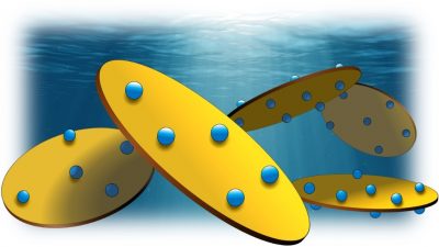
O artigo científico de autoria de membros da comunidade brasileira de pesquisa em Materiais em destaque neste mês é: Reaching Biocompatibility with Nanoclays: Eliminating the Cytotoxicity of Ir(III) Complexes. Malte C. Grüner, Kassio P. S. Zanoni, Camila F. Borgognoni, Cristiane C. Melo, Valtencir Zucolotto, and Andrea S. S. de Camargo. ACS Applied Materials & Interfaces 2018 10 (32), 26830-26834. DOI: 10.1021/acsami.8b10842.
Nanoargilas para superar a toxicidade
Trabalhando em laboratórios do Instituto de Física de São Carlos – USP (IFSC-USP), uma equipe científica desenvolveu uma estratégia que elimina a citotoxicidade (capacidade de destruir células) de um grupo de compostos com propriedades fotofísicas muito interessantes para aplicações na área da saúde. O estudo tornou viável a utilização dessas substâncias, outrora tóxicas, no estudo de organismos vivos e no diagnóstico e tratamento de doenças. Além de eliminar a citotoxicidade, a estratégia modifica algumas propriedades dos compostos, agregando novas funções que podem ser aproveitadas para sensoriamento de oxigênio intracelular e para aprimorar a eficiência de dispositivos luminescentes, como OLEDs.
O trabalho foi reportado em artigo recentemente publicado no periódico ACS Applied Materials and Interfaces (fator de impacto 8,097).
Tudo começou numa conversa informal entre três bolsistas de pós-doutorado ligados a laboratórios do IFSC-USP: Malte C. Grüner e Kassio P. S. Zanoni, ambos ligados ao Laboratório de Espectroscopia de Materiais Funcionais (LEMAF), e Camila F. Borgognoni, do Grupo de Nanomedicina e Nanotoxicologia (Gnano). Zanoni tinha trabalhado com complexos de irídio(III) durante seu doutorado, e desejava aproveitar algumas propriedades desses compostos para utilizá-los como agentes de terapia fotodinâmica. Tal terapia se refere a um conjunto de tratamentos para tecidos doentes, como por exemplo os atingidos pelo câncer, nos quais uma fonte de radiação externa é utilizada para a ativação, no momento apropriado, de um composto inserido dentro do corpo, o qual se encarrega de destruir as células que precisam ser eliminadas.
O desejo do pós-doc Zanoni, entretanto, esbarrava na alta citotoxicidade dos complexos de irídio(III). O pós-doc Grüner, então, teve a ideia inovadora de tentar utilizar laponitas (materiais que ele tinha estudado em seu doutorado) para inibir a citotoxicidade dos compostos. A partir dessa ideia, Grüner e Zanoni realizaram o preparo e a caracterização dos materiais no LEMAF, coordenado pela professora Andrea S. S. de Camargo. No GNano, coordenado pelo professor Valtencir Zucolotto, a pós-doc Borgognoni e a mestranda Cristiane Melo se encarregaram de investigar as interações das nanopartículas com as células.
Estratégia e aplicações
Uma das principais propriedades dos complexos de irídio(III) é a sua intensa luminescência (emissão de luz não resultante do calor) numa ampla gama de cores. Essa característica pode ser útil para iluminar células no interior de organismos vivos em técnicas de bioimageamento, usadas tanto para pesquisa quanto para diagnóstico e tratamento de doenças.
Por sua vez, as laponitas, que são nanoargilas sintéticas totalmente compatíveis com tecidos vivos, têm sido frequentemente propostas na literatura científica como nanoplataformas para transporte de fármacos e de outros compostos dentro de organismos vivos. As laponitas possuem cerca de 25 nm de comprimento e apenas 1 nm de altura.
No trabalho da equipe do IFSC-USP, um novo material foi desenvolvido como resultado da adsorção de moléculas de complexos de irídio(III) na superfície de nanodiscos de laponita.
Os pesquisadores verificaram, no laboratório (in vitro) a capacidade de o novo material ser absorvido por células, sua luminescência dentro das células e sua baixa toxicidade com relação a elas. Para isso, eles utilizaram células de fígado e observaram sua interação com o novo nanomaterial, comparando-a com a interação com o complexo de irídio(III) puro. Os resultados foram sumamente favoráveis aos nanodiscos de laponita com irídio(III), que demonstraram ser inofensivos para as células, além de apresentar boa penetração e alta luminescência – características que os tornam muito adequados para aplicação em técnicas de bioimageamento.

“Neste trabalho, foi demonstrado pela primeira vez que a adsorção de complexos de Ir(III) (em geral, altamente tóxicos) na superfície de nanodiscos de laponita é capaz de extinguir por completo a citotoxicidade desses compostos”, resume o pós-doc Kassio Zanoni, que em 2017 foi vencedor do Young Research Award da SBPMat. “Tal feito torna altamente viável o uso de compostos outrora tóxicos em meios celulares sem prejudicar a integridade do meio e, portanto, tem o potencial de expandir as pesquisas de novos materiais biocompatíveis para uso em mapeamento celular, medicina teranóstica e terapia fotodinâmica”, completa.
De acordo com os autores, o novo nanomaterial poderia agir como uma droga de terapia fotodinâmica, já que, ao ser irradiado com determinados tipos de radiação, produz uma molécula (o oxigênio singleto) que atua na destruição de células cancerígenas. Dessa maneira, o nanomaterial também se torna promissor no campo da medicina teranóstica, a qual propõe a combinação, numa mesma plataforma, do diagnóstico de doenças por bioimageamento com a sua cura por meio de terapias fotodinâmicas.
Além disso, o nanomaterial pode ser usado como sensor para determinar com exatidão a quantidade de oxigênio distribuído no interior de uma célula. “Conforme demonstrado no nosso trabalho, a intensidade da emissão desse nanomaterial é uma variável em função da concentração de oxigênio”, justifica Zanoni.
Por fim, o nanomaterial, na forma de um filme fino nanométrico, também poderia ser aplicado em diodos orgânicos emissores de luz (OLEDs) – dispositivos que já são usados, por exemplo, em telas de celulares. “Isso porque o complexo de Ir(III) adsorvido na laponita agrega propriedades fotofísicas, fotoquímicas e eletroquímicas que são estratégicas para o desenvolvimento de dispositivos mais eficientes”, explica Zanoni.
Esta pesquisa foi realizada com financiamento da Fundação de Amparo à Pesquisa do Estado de São Paulo (FAPESP).
O professor Oswaldo Luiz Alves (IQ – UNICAMP), sócio da SBPMat, foi agraciado com o título de Professor Honoris Causa da Universidade Federal do Ceará (UFC). O título lhe foi outorgado pelo Conselho Universitário da instituição no dia 17 de dezembro de 2018. Além de ser professor titular da UNICAMP, Alves é docente colaborador do Programa de Pós-Graduação em Física da UFC há mais de 30 anos.
Em outubro de 2018, o professor Alves recebeu mais uma importante distinção, a admissão na Ordem Nacional do Mérito Científico na classe Grã-Cruz.