Category: News
XIV SBPMat Meeting received 2,400 abstracts.
With nearly 2400 abstracts submitted, the fourteenth edition of the annual meeting of the Brazilian Materials Research Society (SBPMat) sets a new record in the history of these events.
The term for submitting abstracts was closed on June 15. Until July 10, the authors of the submitted papers will receive their notes of acceptance, rejection or transfer to a different symposium. Abstracts written in Portuguese were refused.
Among the accepted papers, the ones whose authors are undergraduate or graduate students may compete for the Bernhard Gross Award, which will distinguish the best papers in each symposium (one oral presentation and one poster, at most). In order to compete, the authors, after being informed of their approval, must submit an extended abstract, in accordance with the instructions and the model displayed on the site of the event.
This year, the meeting counts with twenty-seven thematic symposia and two workshops, one on nanomanufacturing and the other on organic electronics in the industry, in addition to a symposium entirely organized by students enrolled in the SBPMat University Chapters (UCs).
The UC program at SBPMat was created in March 2014. It mainly aims to gather organized teams of graduate and undergraduate students from scientific and technological fields working in materials area, and officially link them to SBPMat. The activities to be carried out in such program intend to complement the academic development of these students, helping them to organize scientific and technological activities in materials fields, attend events held by the national and international scientific community, and establish exchanges with other UCs unities in the country and abroad.
The XIV SBPMat Meeting will be held in Rio de Janeiro, from September 27 to October 01st, 2015.
About the event
The SBPMat annual meeting is a traditional, international forum, dedicated to recent advances and perspectives on Materials Science and Technology. In the last editions, the event has gathered approximately 1,500 attendees, from the five regions of Brazil and dozens of others countries, for presenting and discussing scientific and technological studies in the field of Materials. The event also counts with plenary lectures, offered by internationally renowned researchers, and an exhibition of interest for the Materials community.
Featured paper. Nanometric Origami: organized strain of two-dimensional materials
Paper: Crystal-oriented wrinkles with origami-type junctions in few-layer hexagonal boron nitride. Oliveira, Camilla K.; Gomes, Egleidson F. A.; Prado, Mariana C.; Alencar, Thonimar V.; Nascimento, Regiane; Malard, Leandro M.; Batista, Ronaldo J. C.; de Oliveira, Alan B.; Chacham, Helio; de Paula, Ana M.; Neves, Bernardo R. A. Nano Research. 2015, 8(5): 1680–1688. DOI: 10.1007/s12274-014-0665-y.

Camilla Oliveira was at the Federal University of Minas Gerais (UFMG), in Brazil, studying samples of hexagonal boron nitrite (hBN) with an atomic force microscope (AFM) within the framework of her doctoral studies in Physics, when one particular aspect of the control samples caught her attention and that of her advisor, Professor Bernardo Neves. After undergoing a heat treatment (annealing), the hBN had gained nanometric wrinkles, arranged in a geometric pattern that seemed to follow some sort of organization.
The researchers decided to study these wrinkles in more detail. They had an important question to answer: was there any relation between the arrangement of the wrinkles and the hBN crystal structure? In other words, did these wrinkles have a crystallographic orientation? Until that moment, there were no records in scientific literature of crystallographically-oriented wrinkles in two-dimensional materials, but this property could be useful.

Camilla and her advisor joined other scientists from UFMG and the neighbor Federal University of Ouro Preto (UFOP) in order to carry out that research. The team produced samples composed of a few layers of hBN anchored on a silicon substrate, they heated them at 1,000 degrees Celsius and then cooled them. During this process, the silicon and the boron nitride displayed opposite strain behaviors. Due to the heating, the hBN contracts itself, while the silicon expands, shrinking the hBN. On the other hand, the cooling expands the hBN and shrinks the silicon, folding the boron nitride as origami paper.
After much experimental work using several techniques and approaches, and various simulations, the scientists were able to confirm that the wrinkles were forming in well-defined directions inside the crystal lattice. Analyzing the folding pattern in details, the scientists noticed the triangular-shaped joints by which the wrinkles (usually three of them) met.

Detail: as proven by the Brazilian scientists, for the crystallographically-oriented folding patterns to be formed, the heat treatment must consist of rapid heating, followed by slow cooling (for example, citing the rates used in the research, 50 °C per minute to heat, and 8 °C per minute to cool). The wrinkles produced with faster cooling rates are arranged in a disorderly manner, with no crystallographic orientation.
The researchers have also concluded that this type of organized strain could happen, not only to hBN, but to other two-dimensional materials as well, such as graphene, and that it could lead to interesting applications in straintronics – the field of knowledge that studies and explores the capacity of some materials to have their properties deeply changed due to strain processes.
The results of the research were recently published on the scientific journal Nano Research.
“In my opinion, the main contribution of the paper is to present a property that may be shared by many two-dimensional materials: the organized strain, i.e., strain in well-defined crystallographic directions, of a material at the nanoscale”, says Professor Neves, who is the corresponding author of the paper.
The research was funded by the Brazilian agencies Capes, CNPq and Fapemig, and by INCT-Nanocarbono.
SBPMat newsletter. English edition. Year 2, issue 5.
|
||||||||||||||||||||||||||||||||||||
Featured paper: Magnetic thin films for miniaturized devices.
Paper: Annealing effects on the microwave linewidth broadening of FeCuNbSiB ferromagnetic films. Alves, M.J.P.; Gonzalez-Chavez, D. E.; Bohn, F.; Sommer, R. L. Journal of Applied Physics. 117, 123913(2015) DOI: 10.1063/1.4915330.

A team of scientists from the Brazilian Center for Research in Physics (CBPF) and the Federal University of Rio Grande do Norte (UFRN) conducted a study on magnetic properties of thin films made of a nanocrystalline material (i.e, formed by nanometric grains) type FINEMET. The conclusions of this scientific research can help produce high quality magnetic materials suitable for use in small-sized devices, such as magnetic random access memories (MRAMs) or nano-oscillators. Results of the study were reported in a recent article in the Journal of Applied Physics.
FINEMET type materials are alloys based on iron (Fe), silicon (Si) and boron (B) with small additions of copper (Cu) and niobium (Nb). They have very good magnetic properties when they are produced by rapid cooling followed by annealing. However, there is not yet an established route that allows obtaining the material having these properties in the form of thin films, which are better suited for miniaturized applications.
In the work of the Brazilian team, magnetic thin films FeCuNbSiB were synthesized at CBPF by scientists from UFRN and CBPF. Samples of the film were analyzed using various techniques such as grazing incidence X-ray diffraction, magnetometry and, in particular, broadband ferromagnetic resonance (FMR). “We explored this technique to the limit,” said Rubem L. Sommer, one of authors of the Journal of Applied Physics paper. “It is powerful and has allowed the study of nanostructured materials with great efficiency,” added the CBPF researcher. Sommer and his team have been contributing to the development of broadband ferromagnetic resonance technique since 2011.
The ferromagnetic resonance technique is used to study the magnetization of the material, measuring the amount of electromagnetic radiation in the microwave range that a particular material absorbs. In the conventional version of this technique, explains Sommer, this absorption is measured at a fixed frequency, and the external magnetic field is varied to tune the equipment in resonance. In the microwave range, the frequency may be between 300 MHz and 300 GHz, and 1 Hz equals 1 oscillation per second. “In the case of ferromagnetic resonance broadband, we scan frequency and the external field, making a direct mapping of the material dispersion relation,” explains Sommer.

Based on the combination of the films analyses obtained by the various techniques, the team of scientists unveiled the mechanisms that are responsible for broadening the ferromagnetic resonance linewidht in the material. “The thinner the resonance line, the higher the quality of the material for applications”, said Sommer. The scientists could conclude that the residual stresses (those who remain in the materials after the elimination of their causes) were causing the enlargement of the resonance linewidth, and that annealing reduced these tensions.
The study reported in the article was funded by Brazilian agencies CNPq and CAPES and was developed mainly in the doctoral research of Marcos Alves held in CBPF and recently defended. The doctoral dissertation of Diego González-Chávez, defended in 2013, was also important for the article, as it allowed the successful development of the broadband FMR technique.
The authors of the article are part of a larger network of collaboration that includes, in addition to researchers from CBPF and UFRN, contributors from PUC-Rio and the federal universities of Santa Maria (UFSM) and Rio Grande do Sul (UFRGS), says Sommer. “I believe that this work, as well as the performance of a network spread over different institutions is a very positive aspect of the current Brazilian scientific and technological research reality”, he said. The network develops research on nanostructured materials and magnetic devices for use at high frequencies. “Our research has always a double bias: basic research to understand the phenomena and application development,” said Sommer.
Scheme of ferromagnetic resonance equipment used in broadband research. The Kepco source feeds the magnetizing circuit (Helmholtz coils) and the signal is measured with a vector Network Analyzer (VNA). The sample is placed on a coplanar waveguide with micrometric dimensions.
Results typical broadband of FMR: microwave absorption curve (color) depending on the field and frequency.
SBPMat´s community people: interview with Israel Baumvol.
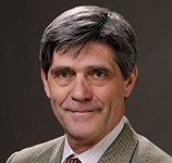
Israel Jacob Rabin Baumvol was born in Rio Grande do Sul, in the city of São Gabriel, in the last day of 1947. When he was a child, he moved to the city of Porto Alegre with his parents and siblings. When he was 19 years old, he entered the Federal University of Rio Grande do Sul (UFRGS) to study Physics. In the following years, in addition to participating in the political activity that occurred in the university against the existing military government, Baumvol dedicated a lot of effort to his studies, trying to reach the academic standard of the bachelor’s degree in Physics of the university. In 1971, he completed the graduation course – without honors, according to him. In the following year, he moved to the city of São Paulo to take a Master’s Degree in the University of São Paulo (USP), in Nuclear Physics and under the orientation of Professor Oscar Sala. In 1975, he returned to UFRGS to undertake his Doctorate, with orientation of Professor Fernando Zawislak, studying composites of perovskite structures. During the doctorate, he became a professor at UFRGS. In 1977, he defended his thesis. For the postdoctoral course, Baumvol chose an institution of industrial research in England, today known as Harwell campus. There, between 1979 and 1981, he worked with techniques of ionic implantation and its applications, mainly the plasma immersion ionic implantation (PIII), and he took part in research contracts with large companies. Due to his expertise in PIII, Baumvol entered the world of the materials for microelectronics, an area in which he made significant scientific contributions and obtained international reputation.
In the United States, Israel Baumvol was an invited researcher of the IBM research center from 1984 to 1988 and, from 1998 to 1999, of the Bell Laboratories, belonging to company Lucent. In France, between 1992 and 1996, he was a visiting professor at the Université Pierre et Marie Curie and at the Université Paris Diderot (Paris 7). In 1997, after coming first in a public entrance examination, he was nominated full professor at Paris 7, but he did not take over the position to stay in UFRGS. From 1995 to 1996, he was a guest professor of the Ruhr Universität, in Germany.
Baumvol was also coordinator of international events held outside Brazil. In 2000 and 2005, he was coordinator (chairman) of international symposia of Physical-Chemistry of silicon oxide and silicon – silicon dioxide interface, organized by the Electrochemical Society. In 2001, he coordinated the International Workshop on Device Technology of the Materials Research Society (MRS), held in Porto Alegre. In 2004, he was meeting chair of the MRS Spring Meeting & Exhibit, that occurs annually in San Francisco (United States).
In 2003, after retiring from his position of full professor of UFRGS, he led the creation of the Materials Science and Engineering Potgraduation Program of the University of Caxias of Sul (UCS), near 130 km far from Porto Alegre, and he was coordinator and researcher of the program until 2014.
From 2002 to 2003, Baumvol presided the Research Support Foundation of the State of Rio Grande do Sul (FAPERGS). More recently, between 2011 and 2013, he was vice-coordinator of the Materials Department in Capes (a federal agency for higher education improvement). Baumvol also coordinated big projects in the Materials segment, such as the first National Network of Research in Nanostructured Materials (2001-2005) and the National Institute of Surface Engineering (2009 to 2010).
Throughout his scientific career, Israel Baumvol has carried out research in subjects related to ionic implantation, thin layer physics and surface modification, in addition to materials for microelectronics.
Baumvol holds the highest productivity level scholarship in CNPq, the Brazilian federal science council. He has authored over 270 peer-reviewed articles, besides books and book chapters. His scientific production has approximately 3,000 citations. He acted as advisor in about 30 Master’s Degree and Doctorate dissertations.
In 2000, he was chosen Prominent Researcher by FAPERGS; in 2010, he was nominated Commander of the National Order of the Scientific Merit by the Presidency of the Brazilian Republic and in the following year, he was named Professor Emeritus by UFRGS. In May of this year, the “Professor Israel Baumvol Microscopy Center” was inaugurated in UCS.
Here is an interview with the scientist.
SBPMat newsletter: – Tell us what led you to become a scientist and to work in subjects of the Materials field.
Israel Baumvol: – It was the junction of three factors. The first one was the desire to use my knowledge one day to be able to contribute to the progress of the country and its citizens. This desire was developed through reading and great political participation during the graduation course. However, seeing as in Porto Alegre the tradition of basic research was very strong and there was nobody working in applied physics, I had a strict academic formation, that was very good for my future. The second factor was my post-doctorate, for which I chose an institution of industrial research, in England. I went there in 1979 to learn ionic implantation, because the institution was a pioneer in this method. There, I became acquainted with ionic implantation, specially its applications, such as reduction of the friction in metallic components (for example Ti-Al alloys) by means of implantation of species and heavy ionic composites, increase of the resistance to wear and corrosion of steel by nitriding, oxinitriding and nitrocarburizing using the method of ionic implantation by immersion in plasma (PIII). At that time, they were constructing there the first industrial-scale reactor of PIII, with a volume of approximately 30 m3, which was later spread throughout the world, including by companies that manufactured these reactors, such as Eaton and several others, including two companies in Brazil. This environment of applied physics fascinated me due to its possibilities. I participated in many research contracts, such as the one about bone prosthesis for a Japanese manufacturer, another about turbine blades for Rolls-Royce and another on cut blades for the future electric shavers project for Philips. These projects, in addition to fascinating me, had a component that for me was romantic: they were confidential projects. The third and last factor occurred by the end of my post-doctorate. I went to a congress in Germany, where I gave a 50-minute lecture, something very difficult nowadays, when the lectures only last about 20 minutes. When I finished speaking and answering questions, there was a coffee break. Dr. James F. Ziegler came up to me, introduced himself and gave me his business card, in which it was written “Research Director, Thomas J. Watson Research Center, IBM”. He invited me to go there because, during my lecture, he thought that the PIII method could solve a serious problem that IBM had with hard drives. Yet again, the siren song of a confidential project. I accepted the invitation and, for some years, during winter and summer vacations, three to four months per year, I went to IBM – Yorktown. There, I got in touch with something unusual for me, the silicon technology, which was just being born. That was yet another allure and my mind was made, Materials Science and Engineering.
SBPMat newsletter: – What are, in your own evaluation, your main contributions to Materials field?
Israel Baumvol: – I worked in many different subjects in my professional activity, some of them mentioned above. I will highlight three of them. The first one was my participation in the beginning of the PIII technology, which is nowadays widely used in the whole world, also in Brazil, where there are at least four services of PIII processes of steel components for the metal-mechanics industry. The second one is my contribution, throughout ten years of work, to explore and to reach the physical limits of silicon oxide as gate dielectric in the metal oxide semiconductor (MOS) technology. I formed a network of cooperation with academic laboratories in four different countries and with industrial laboratories, including IBM, Motorola, Texas Instruments, Bell-Lucent. We reached the physical limit, 1 nm. From there, the entire network started to work on a substitute for silicon oxide, which was the first change in the MOS technology, after forty years. There was a convergence for hafnium oxide and, eventually, certain hafnium-based double oxides. This material stood out, allowing an increase of processing speed and today it is used as gate oxide in advanced processors. It allowed the continuity of the Moore Law, which was threatened. This research segment led to the formation of a golden generation of PhDs, all around gate oxide, which is a crucial subject for the micro and nanoelectronics. Many of them are acting professionally in industrial companies, in technology of silicon and in other activities. Finally, I highlight the creation of a research environment in Materials Science and Engineering and of a post-graduate program in this segment. I started this activity with only one element: Caxias do Sul and its environs possess a large number of industrial companies, small, average and large companies needing research and human resources qualification. Only this, nothing more. Then, from nothing, I gathered some young high-qualified doctors and built the desired research environment, with many excellent laboratories and a very respectable post-graduation program. The impact on the industrial context of the region is notable and very recognized.
Bulletin of SBPMat: – Leave a message for our readers who are initiating their careers of scientists.
Israel Baumvol: – Follow your heart and not convenience. Take advantage of the doctorate, because this is the best time of the career: creative research and free from administrative responsibilities. Do not hesitate in showing your ideas. New ideas are not necessarily bad ideas. Use your post-doctorate to get in touch with the new and the unknown. Do not look for a place that works with the same subject of your doctorate research. Do not hesitate in changing the field, this is very stimulant and constitutes an important factor of individual progress. I pity the professionals who continue working in the subject of their doctorate theses, ten or twenty years after the conclusion. Applied research can very be good research. Get rid of preconceptions, it does not matter if the research is fundamental, or applied or directly industrial. What counts is quality. The only difference is between good quality research or bad quality research.
Interviews with plenary speakers of the XIV SBPMat Meeting: Ulrike Diebold.
Metal oxides display a wide range of properties. Accordingly, they become useful in numerous applications, such as gas sensing, catalysis, protection against corrosion, pigmentation, energy conversion, to name a few. An important detail: in order to comprehend and use these materials, the study of their surface is crucial.

Metal oxides surfaces will be the theme of a plenary talk of the XIV SBPMat Meeting. The speech will be given by Ulrike Diebold, a scientist among the leading experts on the subject in the world. Diebold is engaged in surface science since the time of her doctoral degree, defended in 1990 at the Vienna University of Technology (TU Wien), in Austria. A few years later, during her postdoctoral studies in a surface group at Rutgers University, in New Jersey (USA), she started her researches on titanium dioxide. In 1993, she became a Professor of Tulane University, in the city of New Orleans (USA) and she founded and coordinated a group on surface science. When the group labs were hit by hurricane Katrina in 2005, Diebold was welcomed by several institutions and settled, jointly with some members of the Tulane group, in Rutgers. Finally, she went back to the place where her scientific career had started, TU Wien, as a Professor and coordinator of the surface physics group. With her research groups, Diebold continues to advance in her basic and applied science studies on metal oxides, based, among other techniques, on scanning tunneling microscopy (STM), through which the scientist can investigate these materials at atomic scale.
Ulrike Diebold is the author of more than 180 peer-reviewed articles, which have over 12,000 citations. Her h-index, according to Web of Science, is 52. The scientist has already delivered more than 250 invited talks. Throughout her career, she has received numerous awards and distinctions from several entities such as the Alexander von Humboldt Foundation, American Chemical Society, Austrian Academy of Sciences, Austrian Ministry for Science, Catalysis Society of South Africa, Czech Republic Academy of Sciences, European Academy of Sciences, German National Academy of Sciences Leopoldina, National Science Foundation, among others. She is an associate editor for the Materials Physics Division of the journal Physical Review Letters.
What follows is a mini-interview with this plenary speaker of the XIV SBPMat Meeting

SBPMat newsletter: – In your opinion, what are your most significant contributions in the field of metal oxides surfaces? Please explain them, very briefly, and share references from the resulting articles or books, or comment if these studies have produced patents or products.
Ulrike Diebold: – The field started with the book “The Surface Science of Metal Oxides” by Vic Henrich and P.A. Cox, which was published in 1993 (Cambridge University Press). The book has motivated many people to develop an interest in metal oxide surfaces, and research has progressed tremendously since that time. Some is still valid to this day, e.g., the importance of defects for understanding the properties of oxide surfaces, and how critical it is to master surface preparation. Meaningful investigations can only be conducted on ‘well-characterized’ systems with a known and controlled surface structure. About ten years later, in 2003, I wrote a review that focused only on titanium dioxide, which is a widely-used material both in applications and in fundamental research (Surface Science Reports 48 (2003) 53). This review has received quite a bit of attention. Another decade later a whole issue of Chemical Reviews (vol. 113, 2013) was focused on metal oxide surfaces, which pretty much summarizes the state-of-the art in metal oxide surface research.
SBPMat newsletter: – Comment on the possibilities offered by tunneling microscopy to the study of surfaces, especially metal oxides surfaces.
Ulrike Diebold: – Scanning Tunneling Microscopy, which was invented by Heinrich Rohrer and Gerd Binnig in the early 1980s, has revolutionized our understanding of the nanoworld. One can use this technique for imaging the geometric and electronic structure of a surface at the local scale, atom-by-atom. This is particularly important for oxides, where it is often the irregularities in the lattice that are the most interesting entities, i.e., defects such as missing atoms, interstitials, or impurities. Scanning Tunneling Microscopy is the ideal tool to investigate such defects at the atomic level and to literally ‘watch’ defect-mediated chemical reactions.

SBPMat newsletter: – If you wish, leave a message or an invitation to your plenary talk to the readers who will attend the XIV SBPMat Meeting.
Ulrike Diebold: – I think it is simply exciting to observe phenomena such as defects disappearing from a surface and coming back, or single molecules dissociating or diffusing across a surface. If you want to see beautiful pictures and movies of processes that could potentially be relevant to your own research, please come to my talk.
More
Interviews with plenary speakers of the XIV SBPMat Meeting: Edgar Zanotto.

Glass-ceramics, discovered in the decade of 1950, are produced by the catalyzed internal crystallization of certain glasses containing nucleating elements, and submitted to temperatures from 500 to 1,100 °C. They can present many properties which make of them interesting materials for many applications in the fields of medicine, odontology and architecture, among others.
In the XIV SBPMat Meeting, glass-ceramics will be addressed in a lecture entitled “60 years of glass-ceramics R&D: a glorious past and bright future”. The lecturer will be Edgar Dutra Zanotto, full professor of the São Carlos Federal University (UFSCar), in Brazil, and director of the Brazilian Center for Research, Technology and Education in Vitreous Materials (CeRTEV).
Zanotto became fascinated by glass-ceramics in 1977, when he read the book Glass Ceramics by Peter McMillan, from Warwick University (United Kingdom), while he was completing the graduation course of Materials Engineering at UFSCar. From that moment on, these materials and their crystallization process have been the focus of his studies, first in his Master’s Degree in Physics (USP São Carlos, Brazil) then in his PhD in Glass Technology (University of Sheffield, United Kingdom) and, until the moment, in the research and development projects that he develops with his group in the Laboratory of Glass Materials (LaMaV) at UFSCar.

Edgar Zanotto is author of an important production in science and glass technology. There are more than 200 scientific articles, with approximately 3,500 citations in Web of Science and 5,000 in Google Scholar; 20 book chapters; 17 patent orders; 2 books and 4 prefaces of international books. His H index is 34, according to Web of Science, and 39 according to Google Scholar. Zanotto already received 28 prizes or distinctions from diverse entities, as American Ceramic Society, Elsevier Publishing Company, International Commission on Glass, The World Academy of Sciences and CNPq, the Brazilian Federal Research Foundation. He is Commander of the Brazilian National Order of the Scientific Merit. He was chairman of six of the most important international congresses on the glass area. He gave more than 110 invited lectures and a dozen of plenary lectures. He is editor of the Journal of Non-Crystalline Solids.
Here is a mini interview with this lecturer of the XIV Meeting of SBPMat.
SBPMat newsletter: – What are your most significant contributions or the ones with bigger social impact in the subject of glass-ceramics? Explain them very briefly and comment what was generated from them (papers, books, patents, products, etc.).
Edgar Zanotto: – I believe that the most significant contributions of my research group are referred to tests and improvements of models of nucleation, crystal growth and total crystallization of glasses. Moreover we developed and tested, successfully, models that describe the sintering with concurrent glass crystallization, besides several measurement techniques and theories of dynamic processes (viscous flow, structural relaxation, diffusion and crystallization) in glasses. The numbers of papers, patents and books generated from these researches are described above.

SBPMat newsletter: – Please, name some products made with glass ceramics that are in the market and some possible promising applications.
Edgar Zanotto; – Throughout the last 39 years we develop glass ceramics from iron and steel slags and from recycled glasses – for application in civil construction and architecture – and also more sophisticated materials for odontological and medical use. These will be presented in the lecture.
SBPMat newsletter: – If you wish, leave a message or an invitation to your plenary talk to the readers who will attend the XIV SBPMat Meeting.
Edgar Zanotto: – In the lecture I intend to revise the main models of nucleation and crystal growth in glasses and to discuss their applicability to the development of new glass ceramics. Everything will be illustrated with colorful figures of innumerable new products. I hope that the lecture will be interesting and motivating for the students and researchers (experimental and theoreticians) of the areas of materials science and engineering, and condense matter physics and chemistry.
Learn more:
(Português) Inscrições de solicitação de recursos da FAPESP para participar do XIV Encontro da SBPMat
SBPMat newsletter. English edition. Year 2, issue 4.
|
||||||||||||||||||||||||||||||||||||||