People from the community: interview with the Argentinean scientist Galo Soler Illia.

Galo Soler Illia.
Galo Soler Illia.

How many scientific vocations were aroused, and how many domestic accidents were caused, by experimental chemistry games for children (which until some time ago did not follow all the toy safety standards)? The Argentine scientist Galo Juan de Ávila Arturo Soler Illia belongs to this group. He remembers that his interest in science lit up (literally) with a small fire caused by a chemistry lab set in his parents’ home –  two lawyers, members of the Radical Civic Union, that was also the party of Galo Soler Illia’s grandfather, President Arturo Umberto Illia, who ruled Argentina from 1963 to 1966, until undergoing a coup.

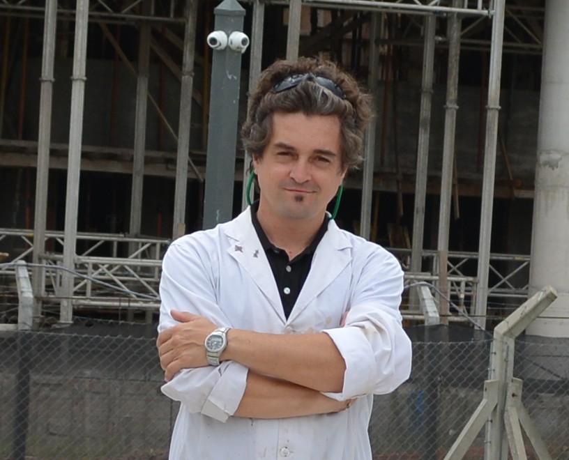
Today, Galo Soler Illia can be considered one of the best known researchers in the Brazil´s neighboring country, both in the scientific community (he is among the 30 Argentine scientists best positioned in Google Scholar for the citations to his works, and has also received the top national science awards) and among the lay public (in the field of Nanotechnology, he is a very active and didactic presenter in all the media, and is usually an information source for Argentine journalists).

Galo Soler Illia was born in Buenos Aires on May 31, 1970. He completed his primary studies in a private constructivist school, Bayard College. In 1983, he enrolled in the National School of Buenos Aires, a public institution dependent on the University of Buenos Aires (UBA), which among other things was characterized by a high study demand, a wealth of extracurricular activities and better-quality infrastructure than other public schools. In 1988, he graduated from the college with a specialization in Sciences. Both in primary and secondary education he had the opportunity to carry out activities in science labs.

In 1989, Soler Illia began to study in a Chemistry Sciences course at UBA. During the undergraduate course, he began teaching in the Department of Physical, Analytical and Inorganic Chemistry of UBA and doing research in a group of Materials Chemistry and also in a laboratory set up in the house of a friend. In 1993, he obtained a bachelor’s degree in Chemistry, with a grade point average of 9.13 / 10.

From 1994 to 1998, Soler Illia completed his doctorate in Chemistry, also at UBA, under the guidance of Professor Miguel Angel Blesa. Through research on nanoparticles of mixed metal hydroxides, he generated knowledge about the complex mechanism of particle formation, which would be very useful in his research as a postdoc and as a professional researcher, focused on the synthesis of materials with high control of their characteristics. Concomitantly to the doctorate, he continued to teach, as an assistant, at UBA.

In 1999, he moved to France, together with his wife Astrid Grotewold, also a chemist, and remained there until 2002. Soler Illia did postdoctoral studies at the Université Pierre et Marie Curie (Paris), under the supervision of Dr. Clément Sanchez, with a 2-year scholarship from CONICET, the main Argentine entity in support of science and technology. In the post-doc, Soler Illia developed methods to produce highly controlled porosity materials. This period resulted in Soler Illia’s most cited articles so far, with more than 1,800 citations in one of the papers, according to Google Scholar. At the end of his stay in France, Soler Illia also worked on applications of mesoporous thin films for the research and development center of the company Saint Gobain.

Galo Soler Illia returned to Argentina in early 2003, at a time when the country was ending great political instability, which caused the Presidency of the Republic to appoint 5 different people in just 11 days. In addition, the country was still under the effects of the severe economic crisis that had reached its peak in 2001. However, Soler Illia was quickly able to enter the research career at CONICET, working at the National Atomic Energy Commission (CNEA) and without wasting time, founded the Chemistry Group of Nanomaterials, which to date operates in the design and development of nanostructured materials. In 2004, the scientist became a professor of UBA in the department where he studied for his bachelor’s degree and doctorate.

In early 2015, Illia became director of the Institute of Nanosystems (INS) of the National University of San Martín, located in the metropolitan area of Buenos Aires. The INS is defined as a space for nanoscience and nanotechnology research, development and creation, whose ultimate goal is to solve priority problems of industry and society in general. At the institute, Soler Illia has a multidisciplinary scientific team of 4 researchers (4 more in 2017), 6 graduate and post-doc students and 1 laboratory technician, and also a management team of 6 professionals.

Currently, in addition to being director of INS, Galo Soler Illia is principal researcher of CONICET and associate professor at UBA. He is a member of advisory boards at the Argentinean Nanotechnology Foundation (FAN) and at the Brazilian National Synchrotron Light Laboratory, and also a member of the editorial board of the Journal of Sol-Gel Science and Technology (Springer). Moreover, Soler Illia has a scientific dissemination column on Nanotechnology  in a television broadcast program called “Scientists Made in Argentina”, which airs once a week on the Argentine public channel. Finally, Soler Illia has just been appointed (November of this year) as member of the Argentine Presidential Council 2030, composed of intellectuals from various fields to advise the president of Argentina, Mauricio Macri.

Soler Illia, whose h-index is 44, has produced over 120 papers published in international scientific journals, with about 11,000 citations, according to Google Scholar. He has supervised 7 completed PhD theses and is the author of 2 dissemination books on nanotechnology. He is also the author of 4 patent applications.

His work was recognized with a series of awards for science, technology, innovation and scientific popularization, among them the main Argentinean awards, like Houssay Award (2006 and 2009), from the Secretary and later Ministry of Science and Technology; the KONEX Award (2013) from the eponymous foundation and the Innovar Award (2011 and 2016) from the Ministry of Science, Technology and Productive Innovation. He also received distinctions from the National Academy of Exact Sciences, FAN, Argentinean Association of Physicochemical Research, CONICET, BGH and Dupont companies, among others. In May of this year, Galo Soler Illia was appointed titular scholar of the Argentinean National Academy of Exact Sciences, Physics and Natural Sciences, a select group of only 36 scientists.

Here’s an interview with the Argentine scientist.

SBPMat newsletter: Tell us why you became a scientist and work in the field of materials.

Galo Soler Illia: I always liked Chemistry. This started when I received a chemistry game, I was five years old, and while experimenting with it I burned my parent`s dinner table. Later, during my high school studies I was a bit of a nerd, writing software code for physics classes at my school. Writing code aroused my curiosity to know how things worked and how problems could be solved. I learned a lot. Near the end of secondary education, I decided to study Chemistry because I believed it was a very versatile and wonderful course that had great possibilities in many fields. At that time, I was really interested in Biotechnology, which was a new area. At the time I started my undergraduate studies at the University of Buenos Aires (UBA), the area of Materials Chemistry had began to emerge. Still a student, I began teaching as an assistant in the Department of Inorganic, Analytical Chemistry and Physical Chemistry of the Faculty of Exact and Natural Sciences, inspired by the example of young and enthusiastic teachers who were returning from abroad and who propagated an atmosphere of work and demand. Together with my best friends, we set up a laboratory on the terrace of one of my friend’s home. There we grew crystals and planned molecule synthesis. Since we spent all day at university and had some spare time, I found a place to work, without a salary or scholarship, in a Materials Chemistry group that had just begun. Everything was very fast, and before I noticed it I had finished my undergraduate studies and began my doctorate, manufacturing microparticles for catalysts. It was a beautiful time of my life, a time from which I still retain my innate curiosity, my willingness to explore and build materials and a wonderful group of friends, who have become outstanding colleagues now spread out throughout the world.

SBPMat newsletter: In your opinion, what are your main contributions to the Materials area, considering all aspects of your scientific activity?

Galo Soler Illia: I have always been interested in building materials, in the chemist’s task to join atom with atom, to manufacture new architectures. I focused on understanding the physicochemical phenomena that take place during the production of a material. When you know and understand these processes, you go from simply “preparing” a material to being able to design it and synthesize it, however complex it may be. And we can take advantage of the properties of the chemical elements to obtain the properties we desire. I’ll give three examples. In my thesis, I studied the precipitation and aggregation of nanoparticles of mixed metal hydroxides, precursors of catalysts. We discovered a very interesting world and were able to contribute to understanding the complexity behind a dynamic particle formation mechanism: the effects of particle shape and structure, the importance of metals coordination in the formation of a mixed phase, the evolution of surface charge and its effect on the stability of a colloid and much more, which helped me in the future as a solid basis for my research. I was fortunate to be able to work with Miguel Blesa, Alberto Regazzoni and Roberto Candal, three excellent Masters who guided me, stimulated and corrected me.

In my second phase, I worked in Paris in the laboratory of Clément Sanchez. I used what I had learned in order to develop methods to produce highly controlled porosity materials, known as organized mesoporous materials. Again, I became interested in the materials formation mechanisms, which are complex because they require controlling the growth of small inorganic species and their self-assembling with micelles. It is a small physical-chemical symphony, which one must learn to play. We had to use, develop and combine many characterization techniques to understand the phenomena taking place and how they controlled the formation and organization of pore systems, the stability and crystallinity of materials, which among others are important variables in the final performance of these solids.

In my third phase, back in Argentina, I set up a research group at the National Atomic Energy Commission in Buenos Aires, and devoted myself to building more complex architectures based on everything I had learned. My best contributions in this regard refer to the use of forces and interactions at the nanoscale to manufacture many different nanocomposites with designed and surprising optical and catalytic properties. All this required new laboratories, training human resources and the transfer of basic science to technologies. Particularly, over the last years we have worked with companies and aspire to generate nanotechnology in Argentina, extending the knowledge of our laboratory to society.

SBPMat newsletter: Briefly tell us about your interaction with Brazil. Do you come here often for collaborations, events, use of labs, seminars? Have you worked with Brazilian groups or in Brazilian laboratories?

Galo Soler Illia: I returned to Argentina in 2003 and I knew right away about what was being developed in Brazil. Since that time, I began developing projects at the National Laboratory of Synchrotron Light (LNLS), which is a beacon for all those who work in Materials in Latin America. The interaction with the synchrotron staff was very important for us to be able to characterize our materials, and we are amazed to see how the installations have improved over the years. A few months ago I had the opportunity to visit the Sirius building, which is simply stunning and which will be a world reference. I also had the opportunity to visit several universities, teaching courses and collaborating in the education of undergraduate and postgraduate students. Furthermore, we created the School of Materials Synthesis in Buenos Aires, which will have its eighth edition in 2017. This school was designed to generate a community of Latin American scientists qualified with skills in the rational synthesis of materials. We started with many Brazilian students, thanks to the support of the Argentinean-Brazilian Nanotechnology Society, which unfortunately has stopped working. It is truly beautiful to see how students from both countries work together in the laboratories and discuss and present their work in “portunhol” [hybrid mixture of Spanish-Portuguese]. From this school, and with the help of several colleagues, collaborative networks are emerging that will undoubtedly provide us with the technological base for larger joint ventures. I travel to Brazil several times a year and always admire the strength of the country to boost local technological development. I hope that after these difficult times, we may continue growing together.

SBPMat newsletter: We always ask the guest being interviewed in this section to leave a message for the readers who are beginning their scientific careers. What would you say to these junior scientists?

Galo Soler Illia: Looking back, I have three recommendations to young scientists. One is to never lose your imagination and your ability to ask questions; the second is to work hard to find the answers, and the third is to make use of the surprises. Sometimes, we train to develop a path and a strategy and we focus on the rigor to demonstrate and formalize what we find. However, it is crucial to know that this path is full of interesting nooks and turns, and sometimes an aspect we hadn’t taken into account opens up a new and unexplored landscape. Newton said that we, scientists, are sometimes like children on the beach, we find a shell that is prettier than the others and we are happy, but there lies before us the vast ocean of truth. My advice is to continually seek our shells, enjoy them and let us come within reach of understanding the wonders of our universe. And always keep in mind that developing science in our continent is a beautiful challenge that will add richness to our countries and well-being to our brothers.

Interviews with plenary speakers of the XV B-MRS Meeting: Ado Jorio (UFMG, Brazil).

Sixteen years ago, working as a post-doctoral fellow at the Massachusetts Institute of Technology (MIT) in the group of professor Mildred Dresselhaus, the Brazilian physicist Ado Jorio de Vasconcelos headed a study that would produce the first successful result of the application of Optics, more precisely Raman spectroscopy, in the individual characterization of carbon nanotubes – keeping in mind that nanotube´s walls are just one atom thick, with diameters typically about one nanometer. In the MIT website, the page of Professor Mildred, who has been studying carbon nanostructures at MIT for more than 50 years, reinforces the importance of the work she has carried out with Jorio: 5 of the 6 publications selected by the emeritus professor are co-authored by Jorio.

When Ado Jorio began his postdoc he was 28 years old and had just finished his doctorate in Physics from the Federal University of Minas Gerais (UFMG). His thesis was on phase transitions in incommensurate systems, conducted under the guidance of Professor Marcos Assunção Pimenta. Prior to that, he earned his bachelor’s degree in Physics, also from UFMG, after studying Electrical Engineering for three years.

After the postdoc at MIT, Jorio returned to UFMG and was later accepted as associate professor of the university in 2002 via a public selection procedure. From 2007 to 2009 he held a position at the Brazilian National Institute of Metrology, Quality and Technology (Inmetro) to develop nanometrology-related activities. In 2010, he became full professor of UFMG and that same year took over the direction of the Coordination of Transfer and Innovation of the University until 2012. In 2013 he was at ETH Zurich (Switzerland) as a visiting professor, carrying out teaching and research activities. In August 2016 he became Dean for Research of UFMG.

Since 2002, Jorio has expanded the subject of his post-doctoral work. He has conducted research in optics and the development of scientific instrumentation, namely the study of carbon nanostructures with various applications. An example of this diversity is a study in which Jorio participates, in which nanotechnology field techniques are used to understand details of the composition of the “Indian black earth”, a highly fertile soil with carbon sequestration potential, which is found in places formerly inhabited by Indians in the Brazilian Amazon.

Jorio holds one of the highest H-index among scientists in Brazil: 74, according to Google Scholar. He is also one of the most cited researchers in the world, evidenced by the inclusion of his name in the latest Thomson Reuters international list, which tabulated 1% of the most frequently cited papers in each knowledge area among all the indexed scientific articles between 2003 and 2013. Jorio is the author of over 180 scientific articles and 20 books or book chapters, and 8 patent applications. According to Google Scholar, his publications combine more than 30,000 citations.

His contributions have received numerous acknowledgments from prestigious institutions, such as the Somiya Award from the International Union of Materials Research Societies in 2009; the ICTP Prize of the Abdus Salam International Centre for Theoretical Physics in 2011, and the Georg Forster Research Award by the Humboldt Foundation in 2015, among many other national and international awards.

In the XV Brazil-MRS (SBPMat) Meeting, Ado Jorio will deliver a plenary lecture on a topic in which he is one of the world’s leading experts, the use of Raman spectroscopy to study carbon nanostructures. The Brazilian scientist will talk about how the technique evolved until reaching the nanoscale. He also promises to reveal some tactics that allow using light, whose wavelength is at least hundreds of nanometers, as a probe to investigate structures of only few nanometers.

See our interview with this member of the Brazilian research community in Materials and plenary speaker at our annual event.

SBPMat Newsletter: – Tell us what led you to become a scientist and work in the Materials area.

Ado Jorio: – It was a winding path! I entered university to study electrical engineering. Back then I played in a progressive rock band, so I looked for scientific research in the area of music. I was told to talk to a teacher at the physics department who enjoyed music, studied acoustics and materials. That’s how my career began and which ended up in materials science.

SBPMat Newsletter: – In your own words, what are your main contributions to the Materials area.

Ado Jorio: – I would say there are two main contributions. The first is in the area of carbon nanotubes, I have shown that optics could be brought to the level of individual nanotubes. This gave way to a very broad research field because there are various types of nanotubes, depending on their diameter and chirality. Before this work, people were studying nanotubes. After this work, people began to study specific types of nanotubes. It would be equivalent to saying that researchers studying the atom then realized that there are different types of atoms. The article that was the linchpin of this discovery was the [PRL86, 1118 (2001)]. The second contribution was the advancement of optics to study carbon nanostructures more broadly. I worked on several fronts, from scientific instrumentation for optical measurements below the diffraction limit, to the study and characterization of defects, approaching materials of interest in soil science, biotechnology and biomedicine. Some key references are the books “Raman Spectroscopy in Graphene Related Systems” and “Bioengineering Applications of Carbon Nanostructures”.

SBPMat Newsletter: – We always invite the interviewee to leave a message for the readers who are beginning their scientific careers. Many of these readers would like to one day achieve an H index like yours. What do you say to them?

Ado Jorio: – Make a big effort to attend conferences and make great presentations, always! Science is a debate and you have to be heard. Never repeat the same presentation. Each public requires a specific focus. Of course this advice depends on funding, but since the beginning of my career I have always spent my own money to fund my travels, and I still do this.

SBPMat Newsletter: – Leave a message or invitation to your plenary lecture for the readers who will participate in the XV Brazil-MRS (SBPMat) Meeting.

Ado Jorio: – After all of the above, and since the title and abstract are available, I can only offer my thanks to those who will honor me with their presence. It will be an honor to have these colleagues in the auditorium.

————————

Link to the summary of the plenary lecture of Ado Jorio: http://sbpmat.org.br/15encontro/speakers/abstracts/7.pdf

Postdoctoral Fellowship in Energy Science, Nanotechnology, Materials in the USA (Deadline: 30 Oct 2015).

The Consortium for Innovation on Nanotechology, Energy and Materials (CINEMA) aims to foster collaboration between Brazil and the United States in renewable energy and nanotechnology. Over 50 professors and researchers are looking to mentor and host Brazilian postdocs at US institutions.

A competitive stipend starting at US$ 44,310 will be offered to selected candidates for 1-2 years through Brazil’s Science without Borders program and the State Funding Agencies.

The CINEMA program is administered by the Renewable and Sustainable Energy Institute (RASEI), a joint institute between the National Renewable Energy Laboratory (NREL) and the University of Colorado Boulder.  Sponsors include MCTI, CNPq, CNPEM, and CONFAP.

Opportunities for fellowships exist at NREL, MIT, Stanford, the University of Colorado Boulder, Colorado School of Mines, and Colorado State University.

Check the website for details including research areas and how to apply: http://www.colorado.edu/rasei/cinema/application-information.

The next deadline is October 30, 2015 and occurs twice-yearly (February and October).

Interviews with plenary speakers of the XIV SBPMat Meeting: Nader Engheta.

Photo of Prof. Nader Engheta superimposed with some of the images related to his research. Credit: University of Pennsylvania photographer Felice Macera.

Materials created by applying the state-of-the-art in materials science and engineering and nanotechnology can make light and other electromagnetic waves behave in an extraordinary way, becoming very useful for applications in several fields.

To talk about this issue in the XIV SBPMat Meeting, Professor Nader Engheta (University of Pennsylvania, USA) will be in Rio de Janeiro in the end of September. Engheta is a recognized world leader in research on metamaterials – man-made materials created through micro or nanoengineering, and capable of interacting with electromagnetic waves in ways not found in nature.  Metamaterials can sculpt the waves in order to achieve unconventional light-matter interaction.

In Rio de Janeiro, Engheta will talk about extreme scenarios generated from metamaterials: light traveling at full speed through artificial structures, one-atom-thick optical devices, metamaterials that perform mathematical operations, miniaturized circuits – optical rather than electronic – composed by metamaterials, and structures with effective refractive index near zero.

In his childhood in Tehran (capital of Iran), Nader Engheta developed a special curiosity to understand phenomena related to waves. This curiosity propelled him to attend and get a BS degree in Electrical Engineering at the University of Tehran. In 1978, he came to the United States to pursue his post-graduate (master’s and PhD degrees), also in Electric Engineering, carried in the prestigious Caltech (California Institute of Technology), in the United States. In 1982, he got his PhD diploma from Caltech, with a dissertation in the field of electromagnetism. After a post-doctorate at the same institution, Engheta worked as a scientist in the industry for four years, working again with electromagnetism.  Then he joined the faculty of the University of Pennsylvania in Philadelphia in 1987, and was swiftly promoted through the professorial ranks, and now he is the H. Nedwill Ramsey Professor of Electrical and Systems Engineering, with affiliations in the departments of Electrical and Systems Engineering, Physics and Astronomy, Bioengineering and Materials Science and Engineering.

Owner of an H number of 69 according to Google Scholar, Engheta has more than 21400 citations. Besides being author of 28 book chapters and numerous journal articles and conference presentations, Engheta is coeditor of the book “Metamaterials: Engineering and Physics Explorations”, released in 2006 by Wiley-IEEE publisher. In 2012, he chaired the Gordon Research Conference on Plasmonics.

His contributions to science and engineering have received important recognitions and distinctions from several entities, as the international society of optics and photonics, SPIE (“2015 SPIE Gold Medal”), the international union of radio science, URSI (“2014 Balthasar van der Pol Gold Medal”) and the international professional association of electric and electronic engineers, IEEE (“2015 IEEE Antennas and Propagation Society Distinguished Achievement Award”, “2013 Benjamin Franklin Key Award”, “2012 IEEE Electromagnetics Award”, “IEEE Third Millennium Medal”), among many other entities. He is also Fellow of six international scientific and technical organizations, namely, Materials Research Society (MRS), American Physical Society (APS), Optical Society of America (OSA), American Association for the Advancement of Science (AAAS), SPIE, and IEEE.  Engheta also received several teaching awards.  In 2006 the Scientific American Magazine selected him as one of the 50 Leaders in Science and Technology for his development of metamaterial-inspired optical nanocircuitry.

Here follows an interview with Professor Nader Engheta.

SBPMat newsletter: – In your opinion, what are your most significant contributions on issues related to the topic of your plenary lecture? Explain them very briefly and if possible, share references of resulting papers or books, or comment if these studies have produced patents, products, spin-off companies etc.

Nader Engheta: – I am very interested in light-matter interaction, and in my group we explore different methods in manipulating and tailoring interaction of waves with material structures, both in the optical as well as microwave domains.  I am very excited about all the research topics my group and I have been working on.  Some of these topics include (1) The optical metatronic nanocircuitry, in which we brought the notion of “lumped” circuit elements from electronics into the field of nanophotonics, developing a new paradigm in which material nanostructures may function as optical circuit elements.  In other words, “materials become circuits” working with optical signals.  In this way, nanophotonics can be modularized, in an analogous way as in electronics.  This allows one to perform optical signal processing at the nanoscale, (2) Metamaterials that can do math:  following our work on optical metatronics, we are exploring how properly designed materials (e.g., layered materials) can interact with light in such a way that one can do mathematical operations with light.  In other words, we are exploring the following questions:  Can materials be specially designed to perform analog processing with light at the nanoscale?  As light propagates through such properly designed material structures, would the profiles of the output signals resemble the results of certain mathematical operations (such as differentiation or integration) on the profiles on the input signals?  In other words, can we design materials for specific mathematical operations in order to do “photonic calculus” at the nanoscale?  (3) The extreme scenarios in light-matter interaction: this may include extreme dimensionality, like graphene photonics as the one-atom-thick platform for light manipulation, extreme metamaterials in which material parameters such as relative permittivity and relative permeability attain near-zero values.  This category of materials, which we have named epsilon-near-zero (ENZ), mu-near-zero (MNZ) and epsilon-and-mu-near-zero (EMNZ) materials, exhibit very interesting features in their response to electromagnetic wave interaction.

References:

  • N. Engheta, “Circuits with Light at Nanoscales:  Optical Nanocircuits Inspired by Metamaterials”, Science, 317, 1698-1702 (2007).
  • N. Engheta, A. Salandrino, A. Alu, “Circuit Elements at Optical Frequencies:  Nano-Inductor, Nano-Capacitor, and Nano-Resistor,” Physical Review Letters, 95, 095504 (2005).
  • N. Engheta, “Taming Light at the Nanoscale,”  Physics World , 23(9), 31-34 (2010).
  • A. Vakil and N. Engheta, “Transformation Optics Using Graphene,” Science, 332, 1291-1294 (2011).
  • A.Silva, F. Monticone, G. Castaldi, V. Galdi, A. Alu, and N. Engheta, “”Performing Mathematical Operations with Metamaterials,” Science, 343, 160-163 (2014).
  • M. G. Silveirinha and N. Engheta, “Tunneling of Electromagnetic Energy through Sub-Wavelength Channels and Bends Using Epsilon-Near-Zero (ENZ) Materials,” Physical Review Letters, 97, 157403 (2006).
  • N. Engheta, “Pursuing Near-Zero Response”, Science, 340, 286-287 (2013).
  • A.M. Mahmoud and N. Engheta, “Wave-Matter Interaction in Epsilon-and-Mu-Near-Zero Structures”, Nature Communications, 5:5638, December 5, 2014.

SBPMat newsletter: – Help us visualize the metamaterials developed by your group. Please choose one of your favorite photonic materials and tell us, very briefly, its composition, its main properties and its possible applications.

Nader Engheta: – One of the structures developed by my group is the optical metatronic nanocircuits for mid-IR regime (from 8 to 14 microns), in which we properly tailored and constructed nanorods of Si3N4 with specific widths and thicknesses, separated by a specific gap.  These arrays of Si3N4 nanorods function as collections of optical nanoinductors, optical nanocapacitors and optical nanoresistors in mid IR.  We demonstrated that such structures behave as nanoscale optical circuits, with functionality analogous to electronic filters, but here these material structures operate in the mid IR regimes.  We have shown how these structure operate as optical filters in the mid IR, offering exciting applications for future integrated optical devices and components.

Reference:

  • Y. Sun, B. Edwards, A. Alu, and N. Engheta, “Experimental Realization of Optical Lumped Nanocircuit Elements at Infrared Wavelengths,” Nature Materials, 11, 208-212 (2012)

Later, in collaboration with my colleague Professor Cherie Kagan and her group at UPenn, we extended this work into the near IR regime (from 1 to 3 microns).  In this case, we used the indium tin oxide (ITO) as the material of choice, with proper design and patterning of ITO nanorods. We also demonstrated that such ITO-based optical metatronic circuits function as an interesting platform for optical circuitry and filtering.  This can have exciting possibilities in the silicon photonics.

Reference:

  • H. Caglayan, S.-H. Hong, B. Edwards, C. Kagan, and N. Engheta, “Near-IR Metatronic Nanocircuits by Design,” Physical Review Letters, 111, 073904 (2013).

SBPMat newsletter: – If you want, leave a message or invitation to your plenary lecture to the readers that will attend the XIV SBPMat Meeting.

Nader Engheta: – One of the exciting features of doing science is the joy of search for unknowns and the thrill of discovery.  I always believe that we should follow our curiosity and our passion for discovery. Also, in science and technology it is important to maintain the balance between the complexity and the simplicity in search for solutions to scientific inquiry.

More

SBPMat’ s community people: interview with Oswaldo Luiz Alves.

Professor Oswaldo Luiz Alves. (Credits: Gustavo Morita)

It was in the science clubs from the public school and from the neighbourhood, in the city of São Paulo, that Oswaldo Luiz Alves took an interest in sciences during his teenage years, conducting chemistry and biology experiments. At the age of 20, he graduated from one of the first technical courses in Industrial Chemistry in South America, at the Oswaldo Cruz Technical School, relying on a scholarship from the São Paulo State Education Office. During the course, he did an internship at the Biological Institute, ran by the government of the State of São Paulo, where he first got in touch with the infrared spectroscopy technique.

After a one-year experience working in the industry, he was accepted to the undergraduate course in chemistry of the State University of Campinas (Unicamp), and completed it in 1973, obtaining the titles of “bacharel” and “licenciado”. During his undergraduate studies, he acted in teaching and research at the Unicamp´s Institute of  Chemistry. As soon as he graduated, Alves, who was 25 years old at the time, was hired by that institute and, at the same time, started his doctorate, carrying out research on the application of vibrational spectroscopy (both Raman and infrared) in molecular complexes. In 1979, he left for France on a scholarship from the São Paulo State Research Foundation (Fapesp) for a post-doctoral internship, in which he again worked with vibrational spectroscopy. In that opportunity, he could use one of the first Fourier transform infrared spectrometers. Thus, Oswaldo Alves experienced firsthand the beginning of a time in chemistry of fruitful development of new analysis techniques, especially spectroscopic, and their applications. In addition, Alves was also motivated by another movement, which began in the 70s and which occurred mainly in the chemists’ community in Europe: the development and study of new materials within the so-called “solid state chemistry”.

Back in Brazil after almost two years in France, in which he worked as invited professor at the University of Lille, he found a scenario different from the European one. In Brazil, almost no chemist worked in the Solid State area yet. Thus, Alves dedicated himself to introducing the area and, in 1985, he founded the Solid State Chemistry Laboratory (LQES) at Unicamp’s Institute of Chemistry. Since then, the scientist has been making relevant contributions to materials science and technology, in sundry themes such as vitreous materials for telecommunications, two-dimensional materials synthesis techniques, development of integrated chemical systems, purification of carbon nanotubes and interaction between new carbon-based nanomaterials and biosystems.

Currently 67 years old, Oswaldo Alves is a full professor at Unicamp, where he works as a scientific coordinator of the LQES and the Laboratory of Nanostructure Synthesis and Interaction with Biosystems (NanoBioss/SisNano). In his 40 years of teaching, he was advisor to over 50 master’s and doctoral dissertations. He has authored over 200 articles published in scientific journals, which have more than 2,400 citations. He have also authored over 20 patents, 5 of them granted and one licensed, the latter refering to a technology aimed at the remediation of effluents from paper and textile industries. In the scientific dissemination field, he works as scientific editor of two news bulletins, “LQES News” and “Nano em Foco”.

Oswaldo Alves is a member of the Brazilian Academy of Sciences and of the Academy of Sciences of the State of São Paulo, as well as a commander of the Brazilian National Order of Scientific Merit. He is also a fellow of TWAS (The World Academy of Sciences for the advancement of science in developing countries) and of the Royal Society of Chemistry. He has received awards from different entities, such as Unicamp, the Brazilian Association of Chemical Industries (Abiquim) and the Brazilian Society of Chemistry, which he chaired from 1998 to 2000, in addition to being a founder and first director of its materials chemistry division.

See our interview with the scientist.

SBPMat’s Bulletin: – How did you become interested in science? What led you to become a scientist and work in solid state/materials chemistry?

Oswaldo Luiz Alves: – It has been many years. Before I got into University I took part in science clubs of my public school and my neighborhood in the city of São Paulo (Perdizes district). In the neighborhood’s science club we had a small laboratory with materials donated by one of the grandchildren of scientist Vital Brazil, where we conducted several chemistry and biology experiments. Soon after that, I got an internship at the Biological Institute, as a formal requirement of the Industrial Chemistry technical course, where I worked with infrared spectroscopy and polarography (dropping mercury electrode) applied to the determination of pesticides. When I got into Unicamp, in 1969, after a period of experience in the industry (Bayer), it was already clear for me that I would continue studying after graduating, which made me engage in research on rare earth compounds, through a research scholarship from FAPESP, already thinking of becoming a university professor and researcher. I went straight to doctorate, withouth having a master´s degree (that was not very common in the 70s in Brazil), working with Raman-laser and infrared spectroscopies and theoretical calculations of molecular force fields. In 1979, I went to France for my post-doctoral internship at the Laboratoire de Spectrochimie Infrarouge et Raman of the CNRS to work with Raman spectroscopy with spatial resolution, SERS and CARS effect and to commission one of the first infrared spectrometers that operated with Fourier transform. At that time, there was in Europe and especially in France (Bordeaux, Rennes and Orsay) an extremely prolific activity in solid state chemistry, within the materials perspective. I was taken away!

Upon returning to Brazil, I saw the opportunity to found the Solid State Chemistry Laboratory – LQES (1985), with a lot of difficulty, for almost all of the Brazilian chemists worked with solutions. Due to that, I migrated to the Physics community, where I remained for approximately 10 years, even getting to the point of coordinating materials-related activities at the famous meetings of the Brazilian Physics Society (SBF) in the city of Caxambu. Since then, I have always been involved in solid state and materials chemistry, taking part in the Optical Fiber Project (Telebras), where I worked with quantum dot-doped glass for telecommunications, glass for non-linear optics and, in the LQES, on activities connected to two-dimensional (lamellar) materials, nanocomposites involving conductor polymers, integrated chemical systems, glass-ceramics and porous glasses, silicon nanoparticles with complex functionalities, carbon nanotubes, graphene oxide and carbon dots. In the last three themes, my efforts are geared towards the study of the interaction between such new carbons with biosystems, from a viewpoint of assessment of the risks of nanotechnologies (regulation).

SBPMat’s Bulletin: – Which are, in your own assessment, your main contributions to the field of materials?

Oswaldo Luiz Alves: – It is always very hard to make such assessments, but I believe that some points could be listed.

In terms of scientific research, my main contributions have been the research works on quantum dot-doped glass and glass for non-linear optics, the development of synthesis techniques of several two-dimensional materials and their intercalation chemistry, the development of integrated chemical systems (conductor polymer glass, semiconductor glass), purification of carbon nanotubes (effect of oxidized debris) and interaction of new carbons with biosystems (protein “corona” effect and aggregation) and silicon nanoparticles with antagonistic functionality for drug delivery.

I created the Solid State Chemistry Laboratory (LQES), a pioneer in solid state chemistry research in Brazil, where I have worked to this day as scientific coordinator. Another contribution that I believe deserves to be highlighted was my work as coordinator of the “Chemistry Program for Electronic Materials” by FINEP (Funding Authority for Studies and Projects) (late 80s). Several of the more important materials research groups that worked, or still work, in Brazil at a high level, in several states, received funding from this successful program. My participation as founder and first Director of the Materials Chemistry Division of the Brazilian Chemistry Society is worthy of mention. I coordinated the FAPESP project that funded the construction of the first line of EXAFS (XAS) at LNLS (Synchrotron Light Brazilian National Laboratory), and I had direct participation in the user formation programs in a spectroscopic technique that had never been used in Brazil. I am currently working as scientific coordinator of the Laboratory of Nanostructure Synthesis and Interaction with Biosystems (NanoBioss/SisNano).

In 2014 I completed 40 years of teaching at Unicamp’s Institute of Chemistry, where I supervised over 50 students (both for master’s and doctorate degrees), many of whom are, today, leaders in research that stand out in the national and international scenario, and who exercise their activities in several Brazilian states.

I have worked as scientific editor of two news bulletins. The first one is the LQES News, a fortnightly publication that has been running for 14 years, with its editorial line connected to the developments in science and technology (general) and innovation and nanotechnologies. The second one is the “NANO em Foco” bulletin, edited in partnership with the Brazilian Agency of Industrial Development (ABDI), published on a monthly basis and running for 7 years, with an editorial line connected to commercial products, risks and regulation of nanotechnologies. In addition to that, I have published, also in partnership with the ABDI, the “Nanotechnology Guidebook (two editions), aimed at introducing nanotechnologies for the general public.

The several systems and materials studied and developed at the LQES have allowed the filing of 27 patents of process and application, including international ones, and a licensing of an innovative technology for the industry. In addition to that, I have taken part, as a consultant, in two processes related to the Program of Economic Subvention for Companies (Nanotechnology) by FINEP, which led to the development of 8 commercial products.

Along these many years, I participated in several activities connected to the Brazilian scientific policies, out of which we can highlight: coordinator of  councils (Chemistry) at CNPq and Fapesp. Member of the Deliberating Council at CNPq (2 terms of offices) and of the Nanotechnology Council (MCTI/SisNano) in all of its compositions. I have worked, until this time, as consultant for the nanotechnology segment of the Brazilian Agency of Industrial Development and the Management and Strategic Studies Center (CGEE). I have provided consultancy to the State Council for Science and Technology of the Economic Development, Science, Technology and Innovation Office of the State of São Paulo, for the nanotechnology segment. I am part of the scientific council of APAE São Paulo – a non-governmental organization for prevention and inclusion of people with intellectual disabilities.

SBPMat’s Bulletin: – Leave a message for our readers starting their careers in science.

Oswaldo Luiz Alves: – First of all, I would like to say that a scientific career is fascinating, especially in the times we live in, where paradigms are frequently broken. Another aspect, no less fascinating, is living with the intermulti and transdisciplinarities that, at the same time as they expand our knowledge, point out our limitations. In such relations, it is clear that a sound and in-depth knowledge of concepts, techniques and tools is fundamental. It is a process based on an attitude of openness and the acquisition of a “common language” that allows the interaction of different experts and expertises in the solution of problems, very well identified, in science, technology and innovation. Thus, we must, whenever possible, seek a balance between paper-oriented and knowledge-oriented research stances and, particularly, not forget to make a second reading of our research results, therefore seeking to examine their possible connection with the needs of the Brazilian citizens and of the national development.

Interviews with plenary lecturers of the XIII SBPMat Meeting: Robert Chang (Northwestern University, USA).

Prof. Chang and other developers of Nanocos, a card game that encourages students to learn science concepts and their role at the nanoscale.

Robert Chang is a Professor of Materials Science and Engineering at the first materials science academic department in the world, created more than 50 years ago at Northwestern University, where he is also director of the Materials Research Institute.

He holds a Bachelor of Science in Physics from Massachusetts Institute of Technology (MIT) and a Ph.D in Plasma Physics from Princeton University. He spent 15 years performing basic research at Bell Labs (Murray Hill). During the past 28 years at Northwestern University, he has directed several National Science Foundation (NSF) centers and programs in materials research and education.

Prof. Chang was the president of the Materials Research Society (MRS) in 1989. He is the General Secretary and Founding President of the International Union of Materials Research Societies (IUMRS). He has received many distinctions for his work, such as the Woody Award from MRS in 1987, the Siu Lien Ling Wong Fellow from the Chinese University of Hong Kong in 1999, and the NSF Director’s Distinguished Teaching Scholar Award in 2005. He is fellow of the American Vacuum Society and MRS, and honorary member of Materials Research Societies of India, Japan and Korea.

He is (co)author of 400 peer reviewed journal articles, with near 13,000 citations, and h-index of 56.

Read our interview with the plenary speaker.

SBPMat newsletter: – Under your viewpoint, which are your main contributions in the field of Materials Science and Engineering?

Robert Chang: 1. Plasma processing of semiconducting materials;

2. Carbon based materials, such as diamond, fullerene, and carbon nanotubes, and their related devices;

3. 3rd generation solar cells;

4. Infrared plasmonics and sensors;

5. Thin film oxides for electronic and photonic devices.

Top publications below.

H. Cao, Y. G. Zhao, S. T. Ho, E. W. Seelig, Q. H. Wang, and R. P. H. Chang. Random Laser Action in Semiconductor Powder. Phys. Rev. Lett. 82, 2278 (1999); DOI:http://dx.doi.org/10.1103/PhysRevLett.82.2278.

Michael D. Irwin, D. Bruce Buchholz, Alexander W. Hains, Robert P. H. Chang, and Tobin J. Marks.p-Type semiconducting nickel oxide as an efficiency-enhancing anode interfacial layer in polymer bulk-heterojunction solar cells. PNAS, vol. 105 no. 8, 2783–2787 (2008); doi: 10.1073/pnas.0711990105.

Q. H. Wang, A. A. Setlur, J. M. Lauerhaas, J. Y. Dai, E. W. Seelig and R. P. H. Chang. A nanotube-based field-emission flat panel display. Appl. Phys. Lett. 72, 2912 (1998);http://dx.doi.org/10.1063/1.121493.

Quanchang Li, Vageesh Kumar, Yan Li, Haitao Zhang, Tobin J. Marks, and Robert P. H. Chang. Fabrication of ZnO Nanorods and Nanotubes in Aqueous Solutions. Chem. Mater., 2005, 17 (5), pp 1001–1006. DOI: 10.1021/cm048144q.

SBPMat newsletter: – And what about your main contributions to science education, especially in Materials Science?  

Robert Chang: – Over the past 20 years, I have led the development of the Materials World Modules program to teach pre-college students about Materials and Nanotechnology: materialsworldmodules.orgnclt.usgsasprogram.orgimisee.net.

SBPMat newsletter: – Please give us a short teaser about your plenary talk at SBPMat meeting. What do you intend to broach?  

Robert Chang: – Mobilizing world-citizens to solve global problems together!

SBPMat newsletter: – Feel free to leave other comments to our readers from the Materials research community, if you want so.  

Robert Chang: – Materials and nanotechnology research and education are the driving force of all future technologies, including energy, environment, health, and security.