|
||||||||||||||||||||||||||
|
||||||||||||||||||||||||||
The comprehensive and diverse range of activities of the program was undoubtedly one of the highlights of the fifteenth edition of the annual event of the Brazilian Materials Research Society, the XV B-MRS Meeting. The organizing committee of the event, led by Professors Ana Flávia Nogueira (IQ-Unicamp, Brazil) and Mônica Alonso Cotta (IFGW-Unicamp, Brazil), envisaged and made possible a technical program consisting of tutorials, laboratory visits, plenary lectures, panel discussions, oral presentations, poster sessions, technical lectures of companies and exhibition stands.
Chairlady of the event Mônica Cotta: diverse themes and formats over 11 hours of sessions.
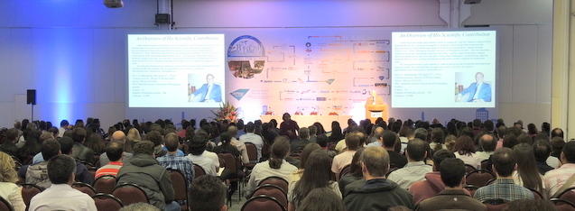
The proposal was overwhelmingly and enthusiastically accepted by the participants of the event, who packed auditoriums, halls and exhibitors area of the convention center Expo D. Pedro, in Campinas (state of São Paulo), to get to know, present and discuss recent advances and perspectives of Materials Science and Engineering. The number of participants registered (about 1,800) exceeded the expectations of the organizing team, given Brazil`s current resource scarcity.
Chairlady Ana Flávia Nogueira: grateful and satisfied with the results achieved in a difficult environment.
The various presentations and interactions during the event were mainly in English, but many different accents could be heard. In fact, the event was attended by participants from 23 countries from North and South America, Europe and Asia. Internationalization was also present in the organization of the meeting, through the symposium coordinators from Canada, Finland, France, Germany, Portugal, Spain, Sweden and USA, and obviously from Brazil.
In the numerous sessions, advances and perspectives were discussed regarding the various types of materials (nanomaterials, biomaterials, two-dimensional, surface and interface materials, electronic organic materials, electroceramics, advanced metals, nanocellulose, semiconductors and superconductors, among other). Not only research but also technology and innovation in materials were included in the presentations and discussions, which covered methods for the discovery of new materials, manufacturing processes, studies on structure and properties of materials, and experimental and theoretical techniques to perform them. There were also countless references to material applications in segments such as energy, health, transportation, packaging, electronics and photonics, and others, including the presentation of cases in which research and development have generated innovation. These moments showed the strong relationship of materials research with the economic growth of countries, with improved quality of life and with the preservation of our planet’s natural resources.
B-MRS president Osvaldo N. de Oliveira Jr: Relationship of materials research with society is stronger than ever.
In fact, it was sustainability that guided the organizers of the event to not print the program books at this year’s meeting. Instead, the participants had a good internet connection and an app that could be downloaded to their mobile devices using a QR code provided at the entrance of the convention center or available in the virtual stores of Google and Apple. The app also included a QR code reader through which participants could obtain the abstracts of the papers presented in the poster sessions.
The XV B-MRS Meeting received support from the Brazilian funding agencies Capes, CNPq and FAPESP, as well as other entities, and sponsorship of the exhibiting companies.
SUNDAY AFTERNOON TUTORIALS AND VISIT TO CNPEM
The intensive schedule began on Sunday afternoon, before the opening of the event, with two tutorials. For nearly 3 hours, more than 200 participants learned about high-impact research, in particular concerning the publication of scientific articles with helpful pointers from Professor Valtencir Zucolotto (IFSC-USP, Brazil). The author of over 140 papers published in international journals, with more than 4,000 citations according to Google Scholar, Zucolotto developed and teaches courses on this subject in Brazil and abroad.
In parallel, in another room of the convention center, about 30 participants hunched over their laptops received theoretical and practical training in computer simulations by professors Pedro Autreto (UFABC, Brazil) and Ricardo Paupitz (UNESP, Brazil).
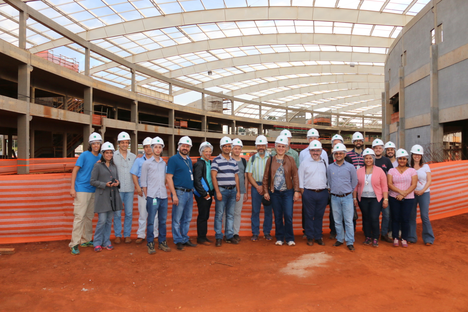
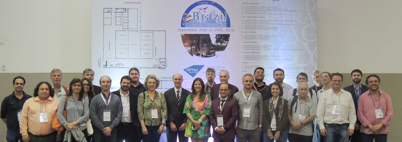
While the tutorials took place at Expo D. Pedro, about 10 kilometers away, a third group of participants of the XV B-MRS Meeting, composed of senior researchers from Brazil and abroad, visited the synchrotron light, nanotechnology and biosciences national laboratories, open to the international scientific community, which comprise the National Center for Research in Energy and Materials (CNPEM). The group also toured the under-construction facilities of Sirius, which will be the second fourth-generation synchrotron light source of the world when it opens before the end of this decade.
SUNDAY NIGHT: OPENING CEREMONY, TRIBUTES AND COCKTAIL
In the evening, at 7:30, almost 700 people occupied the largest room in the convention center to attend the official opening session of the event. “Meetings like this are celebrations of what scientists and technologists can do for the world, for humanity”, said the president of SBPMat, formally opening the XV B-MRS Meeting. On the stage, in addition to Professor Novais de Oliveira (IFSC-USP, Brazil), the table included the chairladies of the event and Professor Roberto Mendonça Faria (IFSC-USP, Brazil) representing the International Union of Materials Research Societies (IUMRS). They thanked the organizers and supporters, whished the participants a good event and announced some information about the event.
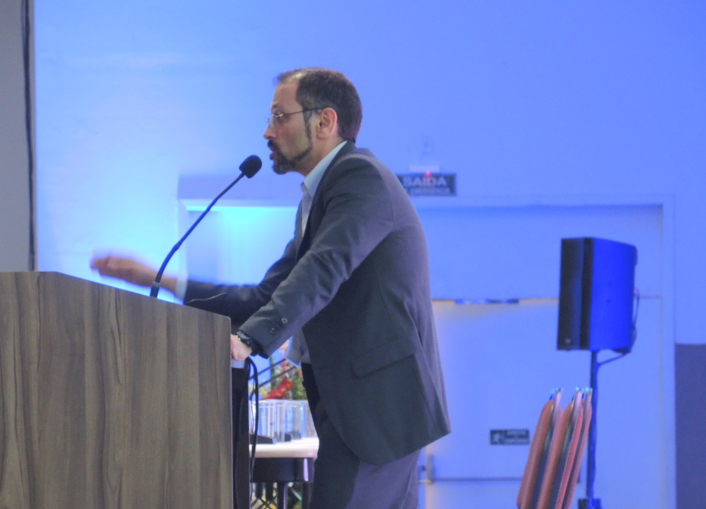
Next, tributes were paid to two scientists, who besides having actively participated in the history of B-MRS, developed international impact studies in the materials field. The first tribute was to Professor José Arana Varela, who passed away last May at age 72. Varela, who made important contributions in the field of ceramics (electroceramics, thin films, nanostructured ceramics, applications in sensors and varistors, among others), was one of the founders and presidents of B-MRS. A former student and friend of Varela, Professor Edson Roberto Leite (UFSCar, Brazil), gave a presentation on the scientific career of his former mentor, highlighting his pioneering work, his international recognition and his success in collaborating with companies. Leite used photographic slides to highlight Varela’s greatest legacy: friends and former students who continue his work. In fact, the next day many of these former students and friends also made a tribute to the master in one of the event symposia (“X Brazilian Electroceramics Symposium – In Honor of Prof. Dr. Jose Arana Varela”).
Before announcing the other tribute at the event opening, Professor Novais de Oliveira Junior took the floor to announce that SBPMat would soon launch its new site and showed a demo version. One of the objectives of the site, explained the president, is to highlight scientific images produced by the materials community, placing them as a background image on all pages, and he then invited those present to send their images.
The second tribute of the night was a distinction that B-MRS awards annually to scientists with outstanding carreer, asking them to present a lecture (Memorial Lecture “Joaquim da Costa Ribeiro”). The scientist elected was Professor Aldo Craievich (IF-USP, Brazil). Argentine, Craievich developed his research career mainly in Brazil and France. In addition to having made outstanding contributions to the study of structures and structural transformations in solids, the scientist was one of the protagonists in the design, construction and operation of the National Synchrotron Light Laboratory (LNLS), located in CNPEM, whose research resources have impacted the international Materials community – mainly the Latin American community. Craievich also participated in the creation process of B-MRS from the very beginning.
In his memorial lecture on advanced materials characterization, Professor Craievich drew attention to a limitation of one of the most widely used techniques to determine the structure of materials, X-ray diffraction. In a historical perspective, he commented on the important discoveries achieved over more than 100 years of using X-ray diffraction. However, the results obtained by this technique, explained Craievich, only show the average of the numerous data captured at the various locations of the sample and in consecutive sampling moments. Therefore, the X-ray diffraction cannot describe situations that are outside the average, but have great influence on the material properties: the material defects and the configurations formed by atoms in motion for very short time scales. These limitations, Craievich commented, began to be overcome with the use of fourth-generation (e.g., synchrotron light sources such as Sirius) and fifth-generation (e.g., the free electron laser) X-ray sources. At the end of a presentation abundant in scientific references, he presented a comic-strip of the famous Argentine cartoonist Quino to prompt future users of advanced X-ray sources to innovate in their experiments, and using photographs he shared some personal memories. See the file of Aldo Craievich´s presentation.
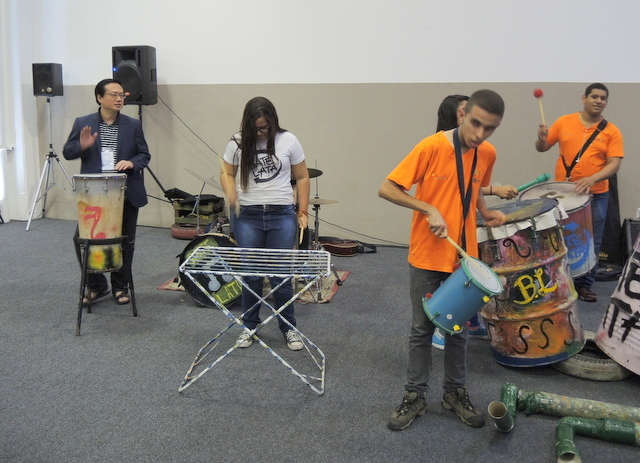
At around 8:45 pm, after the tributes and presentations, music, food and drink awaited the audience at the other side of the doors. Music was provided by the Bate Lata group, made up of children and adolescents associated to a program of sociocultural inclusion through music. The young musicians sang and played well-known popular Brazilian music, using traditional instruments and other instruments manufactured by them from scrap materials (clothesline, oil cans). The cocktail menu (bean broth, drumsticks, croquettes, cold beer and soft drinks) provided the mood of a São Paulo state bar. The confraternization resulted in many encounters and renewed encounters, anticipating the interactions and camaraderie that would reign until the end of the event.
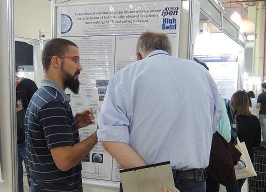
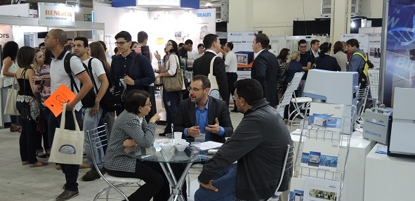
ORAL AND POSTER SESSIONS OF THE SYMPOSIA. EXHIBITORS.
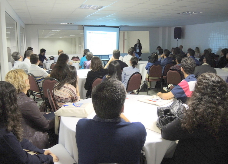
Between Monday and Thursday, more than 2,000 contributions were presented by their authors (undergraduate students to senior researchers) in the 20 thematic symposiums, in the form of posters, oral presentations and invited talks.
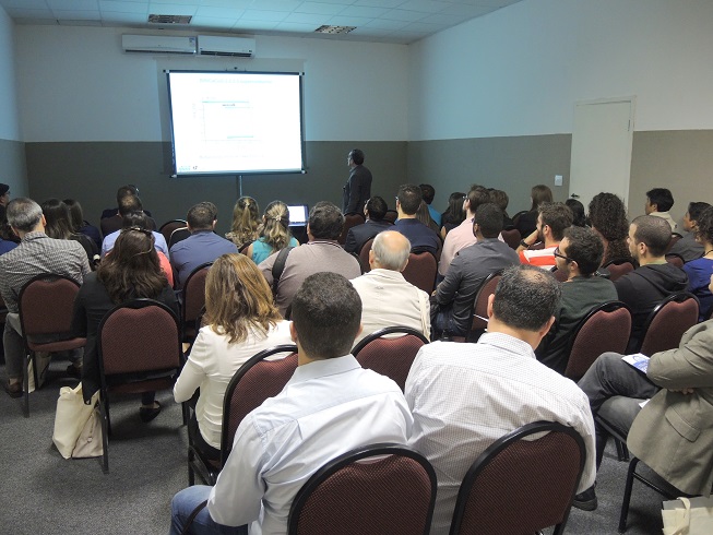

The event program also included two workshops, composed mainly of invited presentations. One was completely organized by students of the University Chapters of SBPMat. Another discussed sustainable development of materials with applications in social impact areas.
At the exhibition, the number of exhibitors set a record in the history of meetings of the society: there were 43 institutions and companies displaying their products and services (mostly scientific instruments) in the stands and in the 12 technical presentations.
DISCUSSION PANELS AT LUNCH TIME
At the time usually designated for lunch, from 12:00 to 2:00 pm, in this edition of the event it was possible to nourish the body while nourishing the intellect with the discussions that took place in the panel discussions.
On Monday, the session organized by the campaign “Research in Germany” of the German government, which also sponsored the snacks, presented research opportunities in Germany. About 80 participants, sitting at round tables, attended presentations of the German Academic Exchange Agency (DAAD), of “Research in Germany” campaign and of researchers who work or have worked in German institutions. First, a panorama of the robust education and research German was presented (thousands of various research institutions, about 2.5 to 2.8% of their GDP invested in R&D, 600 thousand people working in this segment). In the last decade, as it was said, the system has increased the number of foreign researchers – a number that already exceeds fifty thousand. Also shown were several grant opportunities and other resources that can be used by Brazilian academics of all levels of educational training to develop research projects in Germany, as well as the links to find more information. Finally, German researchers spoke briefly about their institutions and research groups on advanced materials, materials for electronics and optoelectronics, and medicine/biomaterials. The “Science Lunch”, as this session was called, ended in a very participatory format: public and speakers seated at the round tables while interacting, possibly about potential collaborations. Six archives of the presentations in this session are available at B-MRS Slideshare.
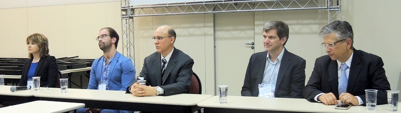
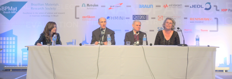
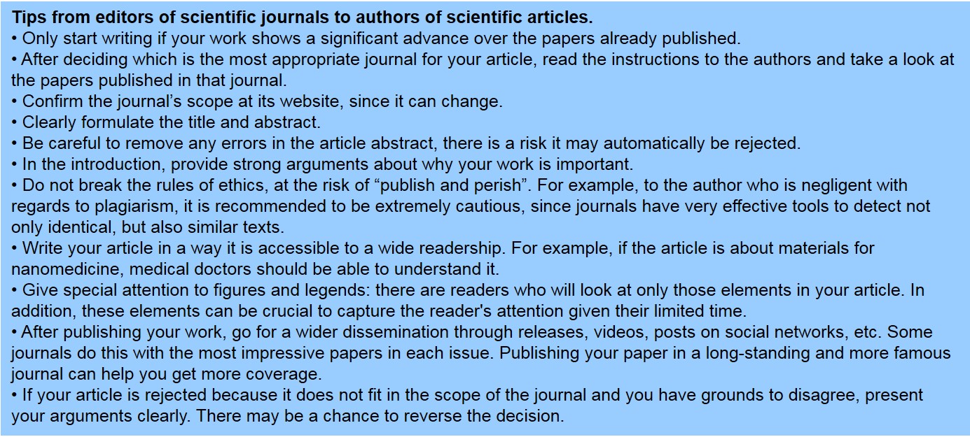
The issue of scientific writing and publication, which had already been discussed Sunday afternoon, resumed on Tuesday at lunchtime. The session, called “Meet the editors” consisted of a discussion panel that brought together a director and the editors-in-chief of scientific journals of the area to talk about the publication of scientific articles. The panelists were: Ifor Samuel (editor-in-chief of Synthetic Metals, from Elsevier, the first journal devoted to organic electronics), Paul Weiss (editor-in-chief of ACS Nano, of the American Chemical Society, impact factor 13,334), Susan Sinnott (chief editor of Computational Materials Science, Elsevier) and Tim Smith (director at the publishing house of the Institute of Physics, IOP). While the audience of about 80 people, savored snacks, sweets, juices and fruits offered by IOP, the editors briefly presented their journals and Tim Smith talked about the set of publications of IOP Publishing in the Materials area. Smith explained that this group of journals recorded a 560% increase in articles downloaded from Brazil in the last 10 years. He also announced that IOP Publishing will conduct a pilot project (experimental) of double-blind peer reviews from January to December 2017, as an option for authors of the journal Materials Research Express. In this mode, the names and affiliations of the authors are removed from the articles before they are sent to the reviewers. The project, Smith said, will be done in response to the demands from sectors of the Materials and Life Sciences communities. A central theme of the speeches of the panelists regarded suggestion to authors who want their articles published (see box). At the end of the session, the panelists answered several questions from the audience.
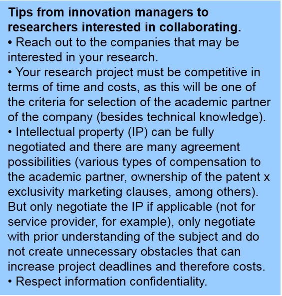 In the discussion on Wednesday, the theme was the contribution of materials research concerning the generation of technological innovation and competitiveness in companies. The theme was addressed with the presentation of Brazilian cases where innovations are generated from research and development projects carried out jointly by university and industrial enterprises. The panel was coordinated by a scholar of technological innovation, Professor Ruy Quadros (Geosciences Institute, Department of Science and Technology Policy, UNICAMP, Brazil). Quadros opened the session by explaining that in the last 15 years, in a slow and continuous process, companies in Brazil have become more innovative. However, he pointed out that resources for innovation (including cultural) in companies are still incipient, hence the important role of public research in the process. Next, the leader of innovation management of Mahle, André Ferrarese, Master in Mechanical Engineering from USP, presented the company: a multinational supplier of systems of the automotive industry, which has 11 technology centers in the world (with 1,950 employees), with one center in Brazil, in the city of Jundiaí (São Paulo state). To launch an average of 4 new products per year, the company begins the process of innovation with about 130 new ideas, which turn into 23 projects. Throughout the process, Mahle collaborates with various international actors: research institutes, universities, suppliers… Ferrarese presented, in particular, the Brazilian case of a consortium in which Mahle participates, which is dedicated to pre-competitive research (knowledge generation and technology development phase, prior to product development). Tribo-Flex (name of the consortium that refers to their study subject, the Tribology of flex engines) brings together automotive companies, including direct competitors like Fiat, Renault and Volkswagen, as well as research institutions and the São Paulo Research Foundation (FAPESP). The goal is to generate and disseminate scientific knowledge on topics of interest to companies. In the context of the consortium, experimental and theoretical studies, tests, courses, presentations at scientific events, and publication of articles were carried out. The origins of the consortium, Ferrarese explained, go back to 2009 when during an international crisis, some Mahle employees took advantage of their reduced work hours to attend university once a week. The relationship between industry and academia was transformed into the exchange of challenges, later into proposals and finally into projects that already have significant results in reducing the problems of engine components, in addition to preparing masters and doctors who can efficiently bridge the gap between industry and academia. See the file of the presentation.
The second company represented in the panel was Braskem, also a multinational company, but born in Brazil in 2002. A major petrochemical in the Americas and world leader in the production of biopolymers, the company has over 300 professionals working in the area of innovation, guided by an international scientific board of experts in areas relevant to the company. The company has already generated over 900 patents. Vinícius Galhard Grassi, leader of Polymer Science in the company, who has a Master`s degree in Materials Engineering and PhD in Chemistry from UFRGS, defended in the panel that both the university and companies are necessary for innovation. “Everyone does their part”, he said, showing in a slide the participation of each actor in the various stages of the innovation process (discovery, basic and applied research, product development and production). Companies need to aim at profit and cannot only promote science, said Grassi. Therefore, skills and resources that would be very costly to maintain internally, such as advanced characterization and frontier knowledge, are acquired at the university, where they already exist. Grassi also presented a series of Braskem’s innovation projects at various stages of development: self-healing plastics, smart polymeric packaging and a new polypropylene resin for producing foams, which after 10 years of project has just been released.
The third and final presentation of the discussion panel was given by Professor Milton Mori, executive director of Inova UNICAMP Innovation agency. Mori told briefly about the agency’s history and results. Inova UNICAMP is dedicated to identifying and promoting opportunities to stimulate innovation and entrepreneurship. The agency provides assistance to researchers in the partnerships with companies, support in the patenting process of inventions and their dissemination and licensing, courses, awards and competitions. It also manages the Science and Technology Park of UNICAMP. Founded in 2003, Inova offers a portfolio of over a thousand patents (of which 13% of the technologies are co-authored by UNICAMP and companies). Mori also highlighted the daughter-companies of UNICAMP (as another way to transform the knowledge generated at the university into innovation), which currently generate nearly 22 thousand jobs, according to the calculations of Inova.
PARTY
On Wednesday night, about 200 participants of the meeting gathered under a different context: the party of the event. The venue chosen was Rudá, a bar and dance hall often frequented by students – an abounding group in Campinas, and particularly in Barão Geraldo, which has several higher education institutions.
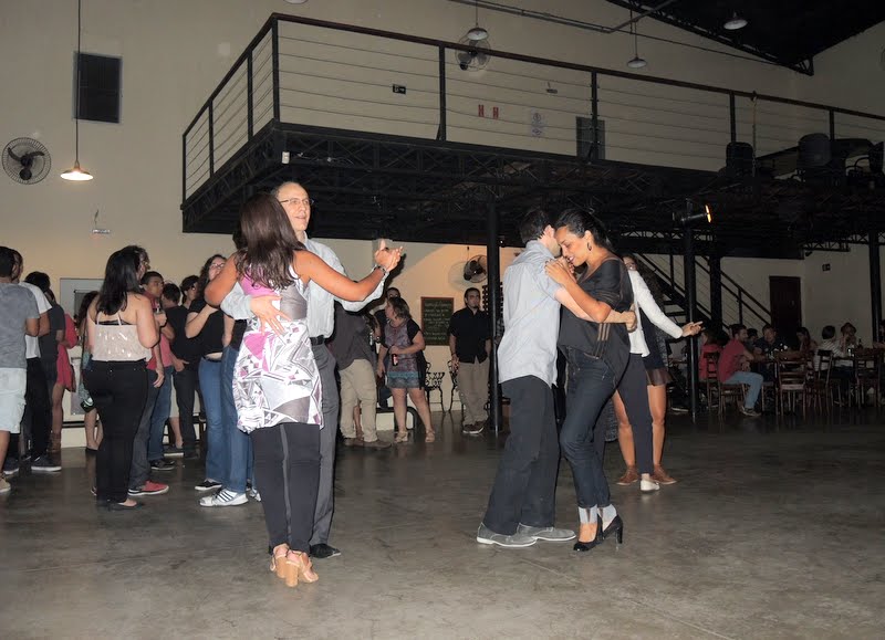
Participants of the event began arriving shortly after 9:00 pm, but the party really started only after the arrival of the B-MRS president, a little before 11:00 pm. In fact, Professor Osvaldo Novais de Oliveira Junior showed that his expertise is not only in science but also at parties. After he talked to the DJ, the party perked up and several people started dancing forró.
The party was attended mainly by the students, but some professors, including some of the plenary speakers were also there.
PLENARY LECTURES
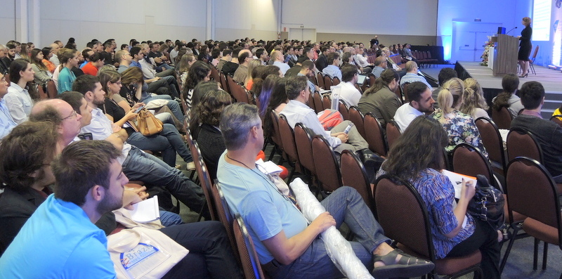
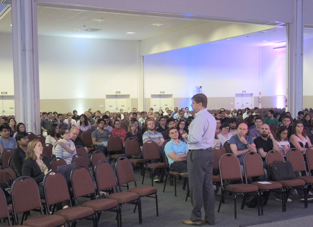
One of the event highlights were the seven plenary lectures, in which scientists who are international protagonists in their research topics presented themes that are at the frontier of knowledge, ranging from basic research to products already on the market. To the satisfaction of the plenarists and organizers of the event, all plenary sessions were assisted by full auditoriums, with nearly 600 participants.
The first plenary of the event was delivered on Monday at 8:30 am by Professor Elvira Fortunato, director of the Materials Research Center (CENIMAT) of the University of New Lisbon (Portugal). Among the many important awards, this year she received the Blaise Pascal Medal for Materials Science from the European Academy of Sciences (EURASC). The speech of the Portuguese researcher focused on two materials for transistors, alternatives to silicon (usually used as semiconductor as well as insulator), that are more environmentally friendly and with some additional advantages. Firstly, Fortunato referred to the metal oxides, such as IGZO and ZTO. Besides displaying excellent performance as semiconductors, she explained, these materials offer high transparency – greatly desirable in displays – among other advantages. Metal oxides are already part of prototype screens that are on the market and which also continue being studied to reduce their manufacturing cost. The second alternative material presented by the speaker was no less than the role of paper, which she used to develop the award-winning paper-based transistor, where cellulose not only functions as a support but also as insulator. Flexible, lightweight, recyclable and cheap, Paper-e® opens up numerous application possibilities, from biosensors made in a common printer to intelligent electronic packaging, which when connected to the so-called “internet of things”, automatically updates the information it displays. To make the paper manufacturing process greener and faster, the CENIMAT group uses bacteria. Within two or three days in vinegar, they produce a nanocellulose which may have distinct properties with respect to plant cellulose, such as the desired transparency. See presentation of Elvira Fortunato.
The afternoon plenary on Monday, delivered by Professor Lei Jiang (of the Technical Institute of Physics and Chemistry – Chinese Academy of Sciences), primarily explained the extreme states of wettability, such as superhydrophobic surfaces, an area where the number of publications has increased dramatically in the last decade. Jiang began his presentation with an introduction about his way of doing research, which can be summarized as learning from nature, by observing it and drawing simple principles (discovery), to then imitate it (invention) and finally transfer this knowledge to industrial applications. Using microscopes and other relatively simple equipment, Jiang and his collaborators have analyzed the structure, in various micro and nanoscale resolutions, of surfaces of natural plants and animals in contact with water or oil, which have properties that are of interest to humans. Examples: the antifogging properties of mosquito eyes, the leaves of rice and lotus that do not get wet or dirty, butterfly wings in which water flows only in certain directions, the cobwebs and cacti that collect and store water efficiently, the underwater superoleophobicity behavior of fish scales. Inspired by these structures, Jiang designs and develops materials (polymers, ceramic thin films, hydrogels, photonic crystals, and others) and very useful devices (for water collecting systems, for water purification or for generating electricity, among many others). These discoveries and inventions have yielded Jiang and his team a collection of patents and publications in high impact journals, such as Nature, Nature Materials, Angewandte Chemie, Advanced Materials, Accounts of Chemical Research, Small and Journal of the American Chemical Society, among others. Moreover, several of the inventions are already circulating in society, outside the laboratory, such as hydro and oleophobic ties and scarves, which always remain clean; tempered-glass installed in public buildings in Beijing that clean themselves thanks to their superhydrophobic surface; water-oil separation systems that traverse the world’s seas in more than 700 ships, and even an innovative printing system, already used to print newspapers, based on materials with special wettability. In developing countries, research, including basic research, must play a role in economic growth, Jiang said in the lecture, referencing an article of the Brazilian physicist José Goldemberg, published in Science in 1998. During the lecture, the Chinese scientist also referred to a principle observed in nature in various Eastern and Western philosophical works throughout the history of mankind (dialectics, ying yang, i ching), the binary systems whose elements cooperate with each other. For this interaction to occur, giving rise to a new phenomenon, said Jiang, the elements must be at a certain distance, the distance of cooperation, which should be considered in the design of smart materials.
On Tuesday, the event program began with a plenary lecture on computer modeling in nano and atomic scales by Professor Susan Sinnot, director of the department of Materials Science and Engineering at Penn State University (USA) and editor-in-chief of the journal Computational Materials Science (Elsevier). Throughout the presentation, Sinnott related the methods available and shared examples of their use in research on MAX phases, nickel-based superalloys, silicon copper-oxide interfaces and deformation of metals. The lecture showed that computational methods help explain the experimental behavior of materials, they are able to make predictions about their properties, help in the discovery of new materials, are critical to design “tailored” materials for certain applications, and also indicate the best routes to manufacture them. At the end of the lecture, professor Sinnott listed some of the limitations to be overcome in order to improve the computational materials science and expand its use, not only in academia but also in industry. For example, make error bars more accurate and more standard, and achieve greater integration in processing, characterization and simulation of materials. See presentation of Susan Sinnott.
A Brazilian scientist, professor at UFMG and with one of the highest H indexes in Brazil (75) was the plenary speaker on Tuesday. Ado Jorio talked about one of his specialities, the characterization of carbon nanostructures by optical techniques (particularly Raman spectroscopy), which, in few words, shed light on matter and measure what happens in the interaction, said Jorio. In these techniques, light is the probe in contact with matter, which he investigates. However, the wavelength of light is at least hundreds of nanometers greater than the study object. This characteristic limits the research… or presents opportunities to go further. Throughout the presentation professor Jorio showed a series of results, from the beginning of this century, in the study of carbon nanostructures, many of these achieved by improving the instrumentation. After sharing tips to enable looking into the tiny intimacy of the carbon structures by optical techniques, Jorio pointed to an interesting branch of his research work. He has participated in studies of the “Indian black earth” found in the Brazilian Amazon, which generally has very poor soil. This soil, however, displays high fertility because of the presence of carbon materials, which remained stable for hundreds of years. Using nanoscience characterization techniques, Jorio and colleagues found particular characteristics on the grain size of these carbon materials. These results can help develop in the laboratory a new black earth that can be used not only in agriculture but also as a way to store carbon sequestered from the atmosphere, where it contributes to global warming. See presentation of Ado Jorio.
On Wednesday morning, the plenary room received the audience with a beautiful photograph of northern lights over the sky of St. Andrews (Scotland) projected onto the video screens. This image anticipated that the speaker, Ifor Samuel, was a professor of the ancient University of St. Andrews (founded in 1413) and that the talk would have much to do with light, specifically with how humans make use of it by means of optoelectronic devices. Optoelectronics, said Samuel, is an area that makes use of the ability of some materials to convert electrons into light and light into electricity, to create devices. In Organic Optoelectronics, the basis of these devices is conjugated polymers, organic materials that can conduct electricity. The discovery and development of these polymers, explained Samuel, was the subject of the Nobel Prize in Chemistry in 2000. Organic semiconductors have interesting features when compared to the conventional ones. They are flexible and light, and are manufactured by means of simple and inexpensive processes, its properties can be adjusted by changing its structure, and they also emit light. With these characteristics, they have numerous applications, some of which are already on the market. One of the best known is the flexible OLED screen, but there are many others and more are yet to come. In his plenary lecture, Samuel presented some new applications of these materials, developed in the Organic Semiconductor Centre at the University of St. Andrews, under his direction. In the area of Biology and Medicine, Professor Samuel showed, for example, a small light emitting device, thin, wearable and disposable, which allows ambulatory treatment of skin cancer by photodynamic therapy. The device has been tested in patients with excellent results both in terms of healing lesions as well as the comfort of treatment. In the communications area, Samuel listed a number of devices for data transmission via LiFi (a type of WiFi which uses a part of visible light of the electromagnetic spectrum to transmit information at high speed). In the field of sensors, he showed polymer lasers that can efficiently detect explosives. Many of the developments achieved by Samuel and his collaborators have generated patents, which are mostly licensed to companies. See presentation of Ifor Samuel.
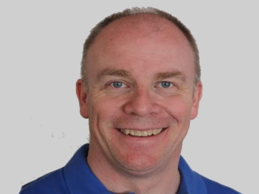
The speaker on Wednesday afternoon was Paul Weiss, distinguished professor of chemistry and biochemistry and of materials science and engineering at UCLA (USA) and founding editor-in-chief of ACS Nano. During the lecture, the audience could know about the skills developed by Weiss, his research group and collaborators for conducting experimental research with molecules, not only to understand their structure and function but also to control them. Paul Weiss shared with the public a series of experiments in which molecules were individually isolated, displaced, placed in controlled environments, stimulated with light, modified, measured and encouraged to form self-assembled structures with specific functions. These scientific achievements have occurred thanks to the knowledge and expertise developed over years of work, and hundreds or thousands of measurements performed on instruments refined by the group. Knowledge and expertise which also helps Paul Weiss to carry out a study project concerning the features and disorders of the brain together with a number of collaborators – including his wife Anne Andrews, responsible for convincing him to devote efforts to a nano and chemical approach of neuroscience.
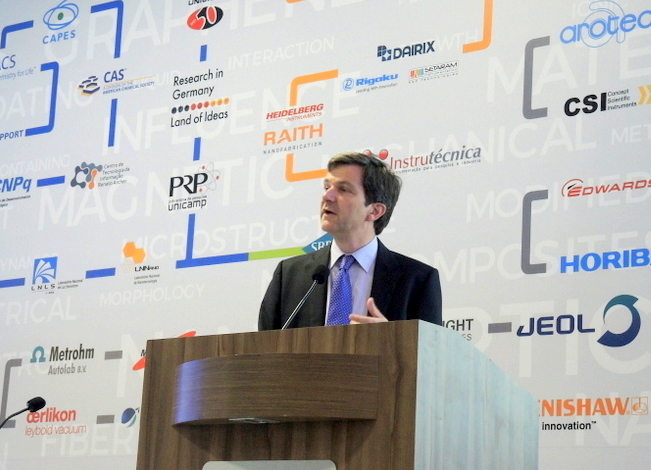
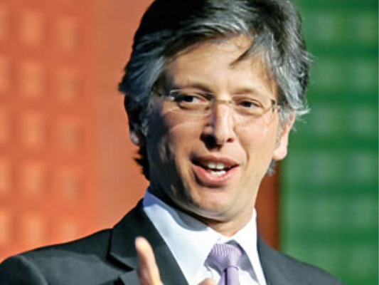
As with all the other lectures, the last plenary lecture of the event clearly exposed the connection of materials research with the needs of society. In this case, the theme was solar cells, devices that produce electricity from sunlight, which is a source of renewable, clean, safe and practically inexhaustible energy. The speaker was Professor Anders Hagfeldt (EPFL, Switzerland), one of the most cited scientists in the world. There are several technologies at different stages of development in the area of solar cells, and they differ mainly by the material responsible for releasing electrons in response to the absorption of photons. In his plenary lecture, Hagfeldt referred to two technologies that are still in the research phase: perovskite solar cells (PSCs) and the dye-sensitized ones (DSSCs). The scientist spoke briefly about the history of the development of both technologies. In the case of DSSCs, the first solar cell with good efficiency in converting light to electricity was done in 1991 and reached the 7.1% mark. Today, 15 years later, the dye used is still the same (it could not be replaced) and its efficiency reached 14.3%. This value is similar to the starting point, 4 years ago, of PSCs, which now reach 22.1% efficiency, but it still does not exhibit stability. If, on the one hand DSSCs cannot replace competing technologies because of their low efficiency, on the other hand, Hagfeldt suggested, they can take ownership of some niches where they make a difference because of their color, low cost and because they are easy to manufacture. In fact, this was the technology chosen to compose kits for homemade solar cells, distributed in secondary schools in Sweden, Hagfeldt’s country of origin. The speaker also showed a number of attempts, some of them very successful, to increase efficiency and stability of solar cells from innovations in manufacture processes and composition of materials, in device structure and in by combinating various materials. See presentation of Anders Hagfeldt.
CLOSING SESSION
The closing session of the fifteenth edition of the annual SBPMat meeting began around noon with a few words and slides by Professor Mônica Cotta. The chairlady highlighted the public rooms full with participants, the packed program, the high participation and interaction of the public and the large number of participants – in spite of the fact that Campinas is not a tourist attraction, she joked. After thanking everyone who collaborated in the organization (SBPMat team, student volunteers) and to all who attended the event, she reminded everyone that the next SBPMat meeting will be in Gramado (RS) and announced that the chairman will be Professor Daniel Weibel (UFRGS).
Then, Professor Osvaldo Novais de Oliveira Junior, representing SBPMat, and Professor Rodrigo Martins, representing the European Materials Research Society (E-MRS) as a former president, signed a cooperation agreement between the two societies to promote scientific collaboration between researchers from Brazil and Europe and in particular to encourage the participation of SBPMat members in the events of E-MRS and members of the E-MRS in the SBPMat meetings, both as participants as well as symposium coordinators.
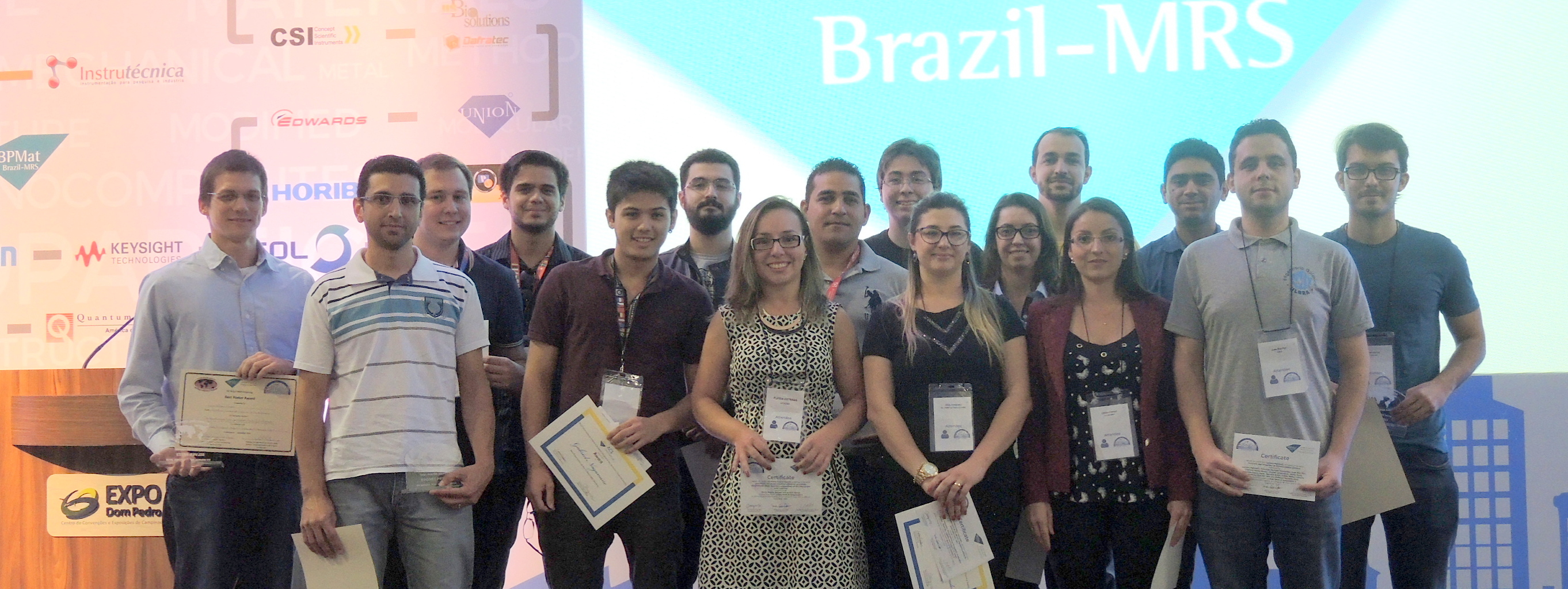
The event ended in a mood of celebration, with the presentation of awards to student authors for the best work presentations of the event. Professor Ana Flavia Nogueira gave thirteen Bernhard Gross awards, granted by SBPMat to the best contribution of each symposium. Then, Professor Cátia Ornelas (UNICAMP), chair of the Brazilian chapter of the American Chemical Society (ACS), gave the ACS awards to the best five works among the winners of the Bernhard Gross award. These students received a cash prize, sponsored by ACS, in addition to the certificate. Then, Professor Elvira Fortunato, representing the E-MRS, announced the winners of the prize offered by the european society to the best works of symposium B (nanocellulose materials). Finally, Professors Roberto Faria and Rodrigo Martins, representing the IUMRS as second vice president and committee coordinator, respectively, handed out the awards granted by that entity to the authors of the best posters of the event related to the sustainable use of raw materials from Brazil. In addition to receiving a trophy and certificate, the three winners were awarded free registration at the next IUMRS event, and the first place will also receive assistance to finance his/her stay. See here the full list of award winners.
SEE YOU IN GRAMADO AT THE XVI B-MRS MEETING! (SEPTEMBER 10-14, 2017)
|
||||||||||||||||||||||||||||||||||||||||||
Dear readers,
We look forward to your participation at the XV B-MRS meeting, to be held in September, 25-29, in Campinas, São Paulo. This year the meeting congregates more than 1500 participants, with 2142 accepted abstracts. Fifteen years after the first annual meeting of SBPMat, as it was called then, our figures are impressive, both for the large number of participants and abstracts as well as for the high quality of the scientific contributions, divided in oral and poster presentations. The current edition of the Annual Meeting covers almost all relevant research areas of Materials Science.
The XV B-MRS Annual Meeting is comprised of 20 Symposia, 2 workshops and 2 Tutorials. The program also includes 7 Plenary Lectures from the most prestigious scientists in cutting edge materials science. The Opening Ceremony will be followed by the Memorial Lecture “Joaquim da Costa Ribeiro”; the renowned scientist Aldo Craievich will talk about the relevance and challenges on advanced materials characterization. Furthermore, in this Meeting program, three discussion panels will take place during lunchtime: Research in Germany, Meet the Editors and Materials Research and Innovation. In particular, the latter will discuss research, development and innovation in industry and the role of innovation agencies and startup ventures.
During the Closing Ceremony, the symposium organizers will honor students with the “Bernard Gross Award” for the best poster and best oral presentations of each Symposium. Awards from the European Materials Research Society (E-MRS) and the American Chemical Society (ACS) will be also granted for best posters and oral contributions.
On behalf of Organizing Committee, we would like to thank the Brazil-MRS staff and board, the funding agencies, the symposium organizers and the local committee members, for their commitment and great effort to make this Meeting possible.
We hope we can all enjoy a very hectic Meeting with stimulating exchange of scientific ideas and results, creating new insights and collaborations, to reach even further quality levels in Materials Science research.
Mônica A. Cotta and Ana Flávia Nogueira
Conference Chairs
 In the late 1950s, solar cells where used for the first time in artificial satellites. Today, these devices that produce electricity from sunlight thanks to the property of some materials to release electrons when absorbing photons, are part of the energy matrix of many countries, besides being used in all sort of spacecraft. Several technologies based on different materials have been developed to make this sustainable production of electricity. However, research in the area is still very intense. While silicon solar cells dominate the current market, other technologies can compete with silicon in economic and environmental terms.
In a plenary lecture at the XV Brazil-MRS Meeting, Anders Hagfeldt, Professor at École Polytechnique Fédérale de Lausanne (EPFL), Switzerland, will talk about recent advances on some solar cells technologies that are alternative to the silicon one, in particular those based on perovskite materials and those based on dye sensitized thin films (known as dye-sensitized solar cells, DSSCs). Hagfeldt has been performing research on both types of solar cells, and succeeded in improving their efficiency using different methods and new materials.
Hagfeldt obtained his diploma of Master of Science in Physics and Chemistry from Uppsala University (Sweden) in 1989 and started his doctoral studies in the same university. In 1993, he concluded his PhD with a thesis on microporous and polycrystalline semiconductor electrodes. Then he went to EPFL, in Switzerland, where he was a postdoctoral fellow with Prof. Michael Grätzel, the inventor of the DSSCs.
In 1994 he went back to his alma mater (Uppsala), first as a junior researcher and then as a Professor in Chemical Physics and Physical Chemistry. He was a Visiting Professor at the Royal Institute of Technology (Sweden) from 2005 to 2010, and at the Institute of Materials Research and Engineering (Singapore) from 2008 to 2010. In 2009, he co-founded Dyenamo, a company dedicated to materials and equipment for solar energy applications.
Since 2014, Hagfeldt is a Full Professor of Physical Chemistry at EPFL, where he heads the Laboratory of Photomolecular Science. Besides, he is a Visiting Professor at Uppsala University and Nanyang Technological University (Singapore). He is a member of the European Academy of Sciences, Royal Swedish Academy of Sciences, Royal Society of Sciences in Uppsala, and the Royal Swedish Academy of Engineering Sciences.
Anders Hagfeldt´s was ranked in various international lists of highly cited researchers, such as the Thomson Reuter’s list of the top 1% most cited in Chemistry (2014-2016) and the top-100 material scientists of the past decade by Times Higher Education (2011). In fact, Hagfeldt authored above 400 papers with more than 47.000 citations and has an h-index of 103, according to Google Scholar. Moreover, he is the author of 9 patent applications.
Here follows a short interview with Professor Anders Hagfeldt.
SBPMat newsletter: – Could you state, very briefly, which are the main advantages and disadvantages of the different solar cells technologies, in terms of efficiency, cost and other relevant criteria?
Anders Hagfeldt: – When it comes to different technologies, the very dominant technology has been for long time based on silicon material, the “silicon solar cells”. In terms of market share, I think that around 90% of all solar cells stored in the world are silicon solar cells. They are mainly produced in China. Silicon has always had the advantage of being efficient and very stable, robust, durable. So, you can get, for example, guarantees of lifetime of over 20 years. If you go few years back, it was always said that silicon solar cells were too expensive and that they wouldn´t never be competitive with other energy technologies, such as fossil fuels and so on. However, five years ago, the production volume has increased a lot and the prize has became unexpectedly lower. Actually, silicon solar cells can be considered quite cheap today. Therefore, silicon solar cells are very good. They have good performance at low cost and match the price in kilowatt-hour of other energy technologies such as burning liquid hydrocarbons, for example.
The next class of technology is called “thin-film solar cells”, and it comprises two different materials. One is known as CIGS, that comes from copper indium gallium selenide, which is the material that absorbs sunlight. The other material is cadmium telluride (CdTe). The latter solar cells are manufactured in a big company in the United States called First Solar. Both of these technologies have the promise to be cheaper than silicon technology. They are almost as efficient as silicon: 10% to 15% less efficient. Both materials are disposed in very thin films, so the materials cost is low and, probably, they can be produced cheaper than silicon solar cells. Therefore, the key thing for thin films to be able to compete with silicon is to be a little bit higher in efficiency and scaling up the production.
These are the three main commercially available technologies today. If we go to research activities, the most “hype” at the moment is the perovskite solar cell. It had its breakthrough only four years ago, and during these few four years, it has reached similar efficiencies as thin-film solar cells. That has been the fastest development in solar cells. Perovskite solar cells will probably be cheaper than thin-film solar cells, but they are still in a research stage. The main question mark of perovskite solar cells has been on stability. In that point, we have made some breakthroughs. Two papers of us have been accepted by the Science journal reporting very promising stability data for perovskite solar cells. That is something I will report on the Brazil-MRS Meeting as a key or latest result of perovskite technology. It is very exciting, perovskite solar cells are not fundamentally unstable, they show promising stability. However, there is a lot of work to be done in terms of scaling up and further stability testing and development.
The other technology I will talk about is dye-sensitized solar cells (DSSC), which is also in research or demonstration level. They are lower in efficiency, so, what we look for in that technology today is niche applications. These cells are based on dyes, which means that you can make them in different colors, and use them in windows, buildings and so on. At the moment, DSSC cannot compete with silicon for large scale, but there is interest for buildings, consumer electronics, rechargeable batteries, keyboards and so on.
SBPMat newsletter: – In your opinion, which are the main next challenges in the field of solar cell research and development?
Anders Hagfeldt: – I can divide this answer in two parts.
Firstly, there is still room and it is still important to make solar cells more efficient to lower the cost of the kilowatt-hour produced. There is a kind of dream target I see. This is not really in my expertise, but I listen to more industrial people talking about U.S. dollar cents per kilowatt-hour (how much costs for solar cell to produce a kilowatt-hour). And it seems that now this cost can go down to 4 cents per kilowatt-hour, which is very good, but it could be cheaper. People say that it can go down to 2 cents per kilowatt-hour. The best thing you can do today to lower the cost per kilowatt-hour of solar cells is to try to increase their efficiency. That is where you see the potential of the perovskite solar cells, because they have had such a fast development and they are already at the same level of established technologies. It seems promising that these perovskite solar cells can show even higher efficiencies than the silicon ones. That is a big challenge but I think it is not impossible.
The second thing is that solar cells is intermittent, that means that they only produce electricity when there is sunshine. During nights and evenings, this is a problem. I come from Sweden that is a country where more electricity is needed when there is less sunshine. That means that you also have to find the storage for electricity.
These key challenges are not for solar cell itself, but for the whole picture of solar energy.
More and more solar cells are being used to produce electricity, but that creates problems to the utility grid, because there can be too much electricity when it is sunny day and too little when it is not sunshine. Therefore, we need to work on storage. I think that for small scale, batteries are interesting, but for larger scale, we need to find how to produce fuel from sunlight or from the electricity produced. And that can be hydrogen, that is something people look into a lot, but also for example methanol.
SBPMat newsletter: – Leave an invitation for our readers to attend your plenary lecture “The Versatility of Mesoscopic Solar Cells”.
Anders Hagfeldt: – I am very happy to go to Brazil. I have been around before, some years back, but I am very excited to meet new people to discuss our research at the meeting. Everyone will be very welcome and I will be very happy to discuss all kind of ideas and questions.
——————————–
Link to the abstract of Anders Hagfeldt´s plenary lecture at the XV Brazil-MRS Meeting: http://sbpmat.org.br/15encontro/speakers/abstracts/9.pdf
 Taking precise measurements of atoms and molecules. Accurately control molecules so that they form specific nanostructures or work together to achieve desired results. The nanoscientist Paul Weiss will address this and much more at the XV Brazil-MRS Meeting. Weiss is Professor at the University of California, Los Angeles (UCLA) and editor-in-chief of ACS Nano journal. At the annual SBPMat event, in addition to delivering the plenary lecture, Weiss will also participate in a roundtable to discuss scientific publication along with the public and editors of other journals.
Paul Weiss received his S.B and S.M degrees in Chemistry from the Massachusetts Institute of Technology in 1980, after conducting research in high-resolution laser spectroscopy. His doctoral research, also in Chemistry at the University of California at Berkeley, was about excited atom reactions in crossed molecular beams.
In 1986, the year he concluded his PhD, his advisor, Yuan T. Lee, was awarded the Nobel Prize in Chemistry for his contribution to the study of the dynamics of chemical elementary processes. Soon after his doctorate, Weiss began working at Bell Laboratories as a post-doc studying the effects of surface chemistry and gas-surface collisions on semiconductor surface electronic properties. In 1988, he worked at IBM Almaden Research Center, where he remained as a visiting scientist until the following year. There his work was on scanning tunneling microscopy (STM) with one of the STM pioneers, Donald Eigler. STM, which lead to a major breakthrough in nanotechnology by enabling the manipulation of individual atoms and molecules, would become one of Weiss’s favorite techniques.
In 1989, Weiss joined the faculty of Pennsylvania State University (PennState), where he continued his work with STM, expanding the technique and studying atoms and molecules. From 2001 to 2002 he was the director of the Center for Molecular Nanofabrication and Devices of PennState. In 2005 he was designated Distinguished Professor of Chemistry and Physics departments at the university.
It was also at PennState that Weiss met the scientist Anne Andrews, with whom he is married to this day. Andrews was responsible for convincing Weiss to apply his expertise and knowledge on nanoscience in the study of the human brain. In this field, and in collaboration with Andrews and other scientists, Weiss has been committed to developing tools to study the interactions between neurons, which take place through electrical and chemical signals in nanometric spaces.
Concomitantly, Paul Weiss participated in the creation of the scientific journal ACS Nano (2015 impact factor of 13,334) and has been editor in chief since the journal’s first edition, published in August 2007. In 2008, the journal received a major distinction, the PROSE Award for Best New Journal in Science, Technology, and Medicine from the Association of American Publishers.
In 2009, he joined the University of California, Los Angeles (UCLA), where he was named Distinguished Professor of Chemistry & Biochemistry. Furthermore, he received, until 2014, the Fred Kavli Chair in Nanosystems Sciences and the directorship of the California NanoSystems Institute, a multidisciplinary institute of research and innovation in nanoscience and nanotechnology. Weiss has also been leading at UCLA a research group that gathers together chemists, physicists, biologists, materials scientists, electrical and mechanical engineers and computer scientists.
Paul Weiss was a visiting professor at the University of Washington (1996 – 1997) and at Kyoto University (1998 and 2000). In 2015, he was Distinguished Visiting Professor at the California Institute of Technology, and Visiting Scholar at Harvard University.
Paul Weiss has published over 300 papers and has approximately 20 patents. According to Google Scholar he has an h-index of 60 and more than 16,000 citations. He has given over 600 invited, plenary, keynote, and named lectures. Weiss has received many awards and distinctions for his research, teaching and scientific publishing. He is an elected senior fellow of IEEE, an elected fellow of the American Chemical Society, the American Physical Society, the American Association for the Advancement of Science, and the American Vacuum Society, and an honorary fellow of the Chinese Chemical Society.
He is currently Distinguished Professor in the Department of Chemistry & Biochemistry and the Department of Materials Science & Engineering at UCLA. He is also Visiting Professor at Nanyang Technological University and continues to work as editor in chief of ACS Nano. Paul S. Weiss also holds a UC Presidential Chair at UCLA.
Here is a brief interview with this speaker of the XV Brazil-MRS Meeting:
SBPMat newsletter: – In your opinion, what are your main contributions on the themes of your plenary lecture? Could you also share with us a couple of references pertaining to publications on these subjects?
Paul Weiss: – In our work, we explore the ultimate limits of miniaturization. We have assembled and operated the smallest switches and motors in the world. To do that, we have put together two sets of capabilities. First, we designed and applied new microscopes and microscopies that can simultaneously measure structure, function, and spectra, with submolecular resolution. In the other, we have developed the ability to place individual molecules into precisely controlled environments. We combine these to understand functional mechanisms and to design new molecules and assemblies to test our ideas.
Try these papers:
Controlling Motion at the Nanoscale: Rise of the Molecular Machines, J. M. Abendroth, O. S. Bushuyev, P. S. Weiss, and C. J. Barrett, ACS Nano 9, 7746 (2015). (Abstract or Article or PDF)
Molecular Switches and Motors on Surfaces, B. K. Pathem, S. A. Claridge, Y. B. Zheng, and P. S. Weiss, Annual Review of Physical Chemistry 64, 605 (2013). (Abstract or PDF)
From the Bottom Up: Dimensional Control and Characterization in Molecular Monolayers, S. A. Claridge, W.-S. Liao, J. C. Thomas, Y. Zhao, H. Cao, S. Cheunkar, A. C. Serino, A. M. Andrews, and P. S. Weiss, Chemical Society Reviews 42, 2725 (2013). (Abstract or Article or PDF)
SBPMat newsletter: – You are part of the team that created ACS Nano, launched in 2007, right? Could you tell us which elements you attribute to the success of the journal, reflected in its impact factor and the awards received
Paul Weiss: – Yes, I was the founding editor-in-chief and continue in that role.
We decided to create a forward-looking journal in which we would lay out the challenges and opportunities for the field, in order to guide and to accelerate advances. We felt that while there are many journals that published communications in nanoscience and nanotechnology, there was not a strong journal that published comprehensive work, on which others could build. This situation, we decided, was holding back our field. We set out to find the most diverse set of curious editors from different fields and we set the journal up to be extremely fast and fair to all authors. Only scientists make decisions and it takes at least two scientists to make decisions to decline manuscripts. Our editors have conversations every day on where the field is going and what are true advances. We have made it intellectually stimulating for ourselves and we believe also for our readers. The result is that we can see the real impact on the worlds of science, engineering, medicine, and beyond. We published the technology roadmaps proposing the BRAIN Initiative in the US and beyond and the new Microbiome Initiative. Stay tuned for more!
Nanotools for Neuroscience and Brain Activity Mapping, A. P. Alivisatos, A. M. Andrews, E. S. Boyden, M. Chun, G. M. Church, K. Deisseroth, J. P. Donoghue, S. E. Fraser, J. Lippincott-Schwartz, L. L. Looger, S. Masmanidis, P. L. McEuen, A. V. Nurmikko, H. Park, D. S. Peterka, C. Reid, M. L. Roukes, A. Scherer, T. J. Sejnowski, K. L. Shepard, D. Tsao, G. Turrigiano, P. S. Weiss, C. Xu, R. Yuste, and X. Zhuang, ACS Nano 7, 1850 (2013). (Abstract or Article or PDF)
Tools for the Microbiome: Nano and Beyond, J. S. Biteen, P. C. Blainey, M. Chun, G. M. Church, P. C. Dorrestein, S. E. Fraser, J. A. Gilbert, J. K. Jansson, R. Knight, J. F. Miller, A. Ozcan, K. A. Prather, E. G. Ruby, P. A. Silver, S. Taha, G. van den Engh, P. S. Weiss, G. C. L. Wong, A. T. Wright, and T. D. Young, ACS Nano 10, 6 (2016). (Abstract or Article orPDF)
SBPMat newsletter: – Please leave an invitation to our readers to attend your plenary lecture “Cooperative Function in Atomically Precise Nanoscale Assemblies” in the XV Brazil-MRS Meeting.
Paul Weiss: – I hope you will join me at the XV Brazil-MRS Meeting for a discussion of how we can explore and understand function at the nanoscale and what it teaches us about the world around us.
Link to the abstract of the XV B-MRS Meeting plenary talk “Cooperative Function in Atomically Precise Nanoscale Assemblies”: http://sbpmat.org.br/15encontro/speakers/abstracts/3.pdf
Scientists warn about the need to value investments in science, technology and innovation to resume economic growth.
The board and committee of the Brazilian Research Materials Society (SBPMat) hereby urges the Brazilian Congress to maintain, in the 2017 budget, the investments in Science, Technology and Innovation (STI) at the levels of recent years, before the drastic cuts which took place in 2015 and 2016. We are aware of the joint effort of society to balance the public accounts, but it is unacceptable that the CTI cuts are far heftier than the drop in tax collection and the decline in domestic gross product.
Equally worrying are the cuts in higher education and in the National Post-Graduate System, evidenced by the interruption or reduction of CAPES programs. These are programs that ensure the continuous process of qualified training, leveraging the critical mass of human capital so that the scientific and technological development achieved can effectively influence industrial innovation, increase the added value of national production, and ensure the social and economic well-being of future generations.
In a country like Brazil, which has not yet reached its scientific and technological maturity to be among the developed nations, the contribution of CTI is sometimes overlooked. The extensive production gains in areas such as agriculture and livestock, extraction and mineral processing, which guarantee balancing our trade surpluses, often go unnoticed. Also unnoticed is the excellence of medicine and digital technology, which directly benefits the daily life of society.
Our specific area, research and new materials solutions, is essential for the future of Brazil as a sovereign nation and less susceptible to the interest of other countries. We are the largest producer of quartz and niobium in the world and we are among the largest in rare earths and other strategic minerals of immense commercial value. Our biodiversity offers a countless number of new organic materials that can be applied in health and in industry segments such as energy and electronics.
We know that the consequences of CTI cuts will be devastating. Besides holding back the continuous advances of recent decades, which threaten to scrap laboratories and squander the value already invested, the cuts realized render infeasible the national technology and the formation of human resources, which is vital to promote sustainable development.
Those who believe that cuts in CTI and in higher education have little impact on the lives of ordinary citizens are mistaken. In the short term, these cuts initially have a more apparent effect on the academic communities in the large centers in Brazil. However, the most affected will be the lowest socioeconomic strata in the medium and long term. These strata have no access to imported material, medical treatment and education abroad, which is only available to the privileged class. The underprivileged are the ones who will suffer if Brazil continues with a tenuous and not uneven government policy, which can cripple the structure of science, technology and innovation, arduously built over recent decades.
As an adhering body of the International Union of Materials Research Societies (IUMRS), B-MRS (SBPMat) invites you to follow IUMRS on Twitter. You will be aware of news of the materials field of global relevance and global origins.
Follow IUMRS on Twitter: http://www.twitter.com/Materials_IUMRS.