
|
||||||||||||||||||||||||||||
|
||||||||||||||||||||||||||||
|
|
||||||||||||||||||||||||||||
|
||||||||||||||||||||||||||||
|
Sunday. Tutorial, opening, memorial lecture and welcome.
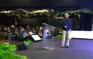
“We made it.” With those words the president of B-MRS opened the sixteenth annual meeting of the society on Sunday, September 10, 2017, at around 7pm. Professor Osvaldo Novais de Oliveira Junior (IFSC-USP) was referring to the difficulties experienced not only by the event organizers but also by all the Brazilian scientific community, in a year which recorded the lowest budget for science and technology in the history of the country.
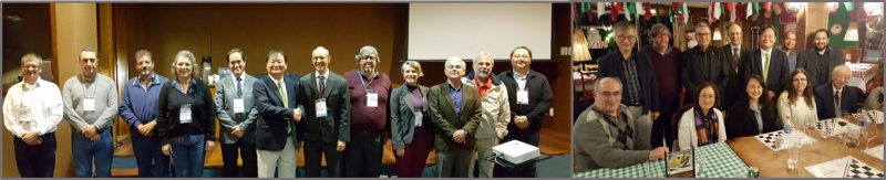
In contrast to this situation, the room that held the opening of the XVI B-MRS Meeting, at the FAURGS event center in the city of Gramado (RS), was nearly full. Close to 900 people were there to celebrate the ceremony. The opening panel assembled on the main stage the representatives of Materials Societies from Latin America, Asia and Europe, as well as the International Union of Materials Research Societies. The composition of the panel table anticipated a point that would be emphasized shortly afterwards in the opening speech and throughout the event in several plenary sessions – the importance of scientific collaboration, not only between different areas, but also between countries, as a source of ideas, resources and skills.
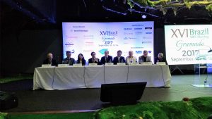
Opening session table. From the left, Robert Chang (general secretary of IUMRS), Hyeongtag Jeon (President of the Materials Research Society of Korea), Claudia Gutiérrez (President of the Mexican Materials Society, SMM), Daniel Eduardo Weibel (Chairman of the event), Osvaldo Novais de Oliveira Jr (President of B-MRS), Soo Wohn Lee (President of the International Union of Materials Research Societies, IUMRS), Roberto Arce (President of the Argentine Materials Society, SAM), Luis da Cunha Lamb (Vice Provost for Research from the Federal University of Rio Grande do Sul, UFRGS) and Rodrigo Martins (Representative of the European Materials Research Society, E-MRS).
After the welcome greetings and wishes for a good event given by the chair of the meeting, Professor Daniel Weibel (IQ-UFRGS), it was time for the traditional Memorial Lecture “Joaquim da Costa Ribeiro”, which name honors and keeps alive the memory of one of the pioneers of Brazilian materials research. The lecture is also a recognition given by B-MRS to researcher every year, highlighting his/her trajectory in the area.
The awarded and speaker of the night, João Alziro Herz da Jornada, was then called to the stage. Jornada, among many other positions, is a retired professor from UFRGS and former president of Inmetro (Brazilian Institute of Metrology Standardization and Industrial Quality). The renowned Brazilian scientist touched on a subject of significant importance in times of funding cuts to science and technology, the relationship between science and innovation and better quality of life. Through news articles recently published in some of the most renowned journals and magazines in the world, Jornada highlighted that this discussion is already the subject of intense and in-depth debate. The Professor presented some models that depict this relationship, either in a simplified, or in a more complex and realistic manner. The honored scientist highlighted some important extra scientific factors for technological innovation: society’s knowledge absorptive capacity, the “learn by doing” practical knowledge entrepreneurial approach, the possibility for entrepreneurs to easily access knowledge, communication and interaction between different agents. To conclude, Jornada asked all researchers to make an effort to systematically and objectively understand the relationship between science and the welfare of society, and thus, to prepare to the discussion on the social and economic impact of science, which is already taking place among the general public.
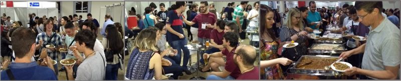
The welcome cocktail awaited the participants at the end of the lecture. Friends and colleagues of the international Materials research community reconnected and socialized around a tasteful dinner of meat, risotto and pasta, as well as beer and soft drinks.
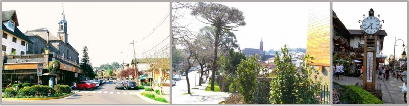
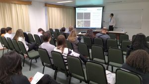
Earlier, in the streets of Gramado, at a temperature of about 30 °C (above average for end of winter at more than 800 m above sea level), the sun was shining and the flowers of the charming city seemed even more colorful. Meanwhile, from 1:30 to 5:30pm, at the event center of FAURGS, more than 200 people benefited from a tutorial on high-impact scientific research – free to participants of the XVI B-MRS Meeting. In the tutorial, Professor Valtencir Zucolotto (IFSC-USP), researcher in the Materials area and creator of online courses on scientific writing and related topics, in an interactive, relaxed and humorous manner addressed the production process of a high-impact paper, from writing to publication in a journal. “The public’s concern to reconcile high-level research with financing difficulties was evident”, commented Zucolotto. Before raffling among the participants two vouchers for a free online course in the platform he created, Zucolotto ended the tutorial encouraging the attendees to engage in high-impact research. “Yes, it’s hard, of course, but with commitment it is less difficult. You cannot be discouraged; there is nothing better than seeing your paper published, divulged and cited,” said the scientist.
From Monday to Thursday: plenary talks, symposia, meetings and party.
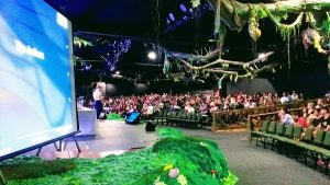
The next morning, at about 8:30 am, the main hall of the event received approximately 600 participants to attend the first of the seven plenary lectures of the meeting, which all had excellent attendance and numerous questions at the end of the lectures.
In the first plenary lecture, Professor Hans-Joachim Freund gave an example of how minute scales can have an enormous complexity. This h=97 index scientist shared his broad and deep knowledge on heterogeneous catalysis (the one in which the phase of the catalyst material is different from the phase of the reagents, for example, catalyst nanoparticles in reactions involving gases). The plenarist captured and held the attention of the public by sharing some of his studies on the topic being carried out in a Berlin research institute dedicated to the study of surfaces and interfaces, the Fritz Haber Institute of the Max Planck Society, where Freund is the director. As the catalysts are very complex materials, Freund said, to understand them at the atomic scale, his research group creates model-systems of increasing complexity and growing resemblance to the actual catalysts. Using instrumentation, computational methods and advanced knowledge of surface science, the group has been able to solve step-by-step the various scientific problems involved in understanding catalysts and as a result develop more reactive catalysts. Despite having all of the Physics Chemistry department (which used to have 80 people and now has 35) allocated to the study of heterogeneous catalysis, Professor Freund joked that he still has a lot of work ahead of him and that to deal with such complexity he would require some 200 researchers!
After the lecture of “Hajo” Freund, the participants distributed themselves in the 15 rooms with parallel programming, dedicated to oral presentations of the 22 symposia – a constant activity repeated throughout the meeting in the mornings and early afternoons. Nearly 2,000 abstracts were submitted to the symposia of the XVI B-MRS Meeting, of which 1,919 were approved for oral and poster presentations. The symposia covered a wide range of research topics in materials, from the study, manufacturing and modification of various materials (polymers, metals, composites, hydrogels, nanomaterials, biomaterials) to its use in the energy, aerospace, health, electronics, bioelectronics, photonics, plasmonics, photocatalysis and other sectors. The manufacturing and safety environmental impact concerning the use of some materials were also addressed in the symposia.

At the end of the oral sessions that morning, as well as on the other days of the event, hundreds of participants, many in small groups, strolled the picturesque streets of Gramado in search of restaurants for lunch. Not a difficult search in this small town that is particularly geared towards tourism, and which concentrates within a few blocks dozens of quality restaurants of different types and different prices, offering international cuisine specialties – from Italian pasta and German pork knuckle to fondue, trout and soups.
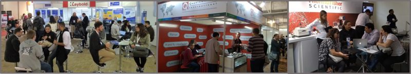
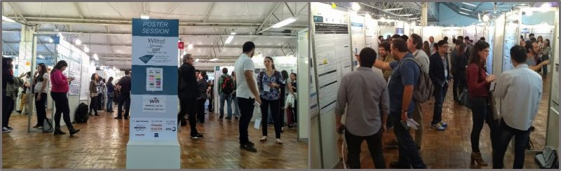
Thanks to the good location of the convention center, by 2 pm the participants were back to the afternoon oral sessions, followed by a plentiful coffee break, quite like the generous morning coffee break, which nourished the participants until the end of the day’s schedule, at around 7:30 pm. The coffee breaks were accompanied by the visits to the stands of the 25 exhibitors that participated in the XVI B-MRS Meeting, distributed around both sides of the coffee break tables.
Also at the beginning of the afternoon, within the activities of the workshop on sustainable development of materials for energy, electronics and transportation, a meeting was carried out on the possibilities for university-industry interaction. The meeting gathered a representative of Umicore – a multinational materials technology and recycling company; an entrepreneur a startup on materials segment (Develop Now) in the Brazilian city of São Carlos; researchers from areas related to sustainable development; the Chairman of the XVI B-MRS Meeting; the President of B-MRS and the general secretary of IUMRS.
The afternoon plenary lecture began at 4:45 pm and was given by Professor Alexander Yarin, of the University of Illinois – Chicago. After highlighting that Brazil is a leading country in materials derived from agricultural waste, the scientist showed that waste from agriculture and fishery can be harnessed to produce biopolymers and in order to manufacture nanomaterials that can be used in a variety of applications. In his lab, Yarin has produced nanofibers, some with very good mechanical properties, from soybean protein, cellulose, gluten, wood components and fish protein, among other wastes. Yarin and his team are currently developing a project to use sugarcane bagasse. The method used is solution blowing, in which a biopolymer solution jet is “blown” by a coaxial air blast. In the interaction between the two jets, the solvent evaporates and the biopolymer acquires a lengthened and thin format. Thus, dry nanofibers are formed which fall on a surface composing tangled fibers, which can finally be presented as something similar to a roll of thin paper. The process can be easily carried out at an industrial scale, Yarin said. The scientist also showed some already demonstrated nanofibers applications, such as the membranes that protect grapevines from the esca funghi, responsible for tremendous grape harvest losses around the world. Another application mentioned was the adsorption of heavy metal ions from contaminated waters, a problem that occurs, for example, in India. Yarin ended his presentation comparing his powerful green nanomaterials to the footballer Pele, who he greatly admires.
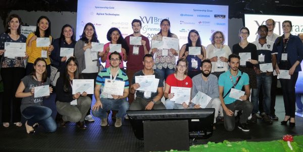
The day’s program ended with an interactive poster session. In three sessions along the event, always taking place at the end of the afternoon, almost 1,400 contribuitions were displayed and discussed. Again, the event provided a QR code for each poster and a code reader in the event app, which was downloaded on 378 mobile devices. By positioning the smart phone in front of the code printed on the poster, the participant could access and save the data from that specific work.
That night it got colder and wetter in Gramado. The next morning, with temperatures at around 13 °C, the participants had to wear winter coats or raincoats to go to the convention center. Fog covered the landscape – typical of winter in Gramado region – which restricted visibility more than 50 meters away.

Inside the convention center, the mood was different. Professor Katsuhiko Ariga (WPI-MANA NIMS and University of Tokyo) received the public in the plenary room expressing his great joy to be there. He had been invited to give a plenary lecture two days before to replace Professor Susan Trolier-McKinstry who could not travel for reasons beyond her control. Ariga’s humorous plenary began with a hot theme, molecular machines, last year’s Nobel Prize in Chemistry. The Japanese scientist (h=144 index) showed a race of nano cars created by scientific teams from different countries with just one molecule, each with a particular format. Ariga also showed other molecular machines developed by him and his group, such as nanopliers that open and close in reaction to movements made by human hands. How is this done? Through a simple equipment these macroscopic human hand movements cause compression and expansion of an air and water medium where the nanopliers are in the interface, causing the molecules to reconfigure again and again in the form of opened or closed pliers. The lecture ended with the image of a future in which we humans will perform nanotechnology with our hands in our day-to-day routine.
Perhaps wondering how this world predicted by Professor Ariga will be, the participants left the plenary hall toward the oral sessions of the symposia, and also to the technical lectures on materials characterization, manufacturing and modification techniques that were given by experts from instrumentation companies in the mornings and afternoons of Tuesday and Wednesday.
In an increasingly damp Gramado, alternating between fog and rain, the second plenary session began. Professor Kenneth Gonsalves (Indian Institute of Technology Mandi, IIT Mandi) led the public toward the ever current theme of chip miniaturization. This trend, explained the researcher, has brought superior performance and lower costs to the infinite range of products that use chips, from everyday electronic devices to health care, transportation and defense devices, among others. To have a sense of sizes, in 2012 the 22 nm node technology was launched (which means that the gate controlling the passage of electric current in the integrated circuit has this dimension). Two years later, the 14 nm node technology was introduced, and in 2016 the 10 nm node. For 2018, the launch of the 7 nm node and, two years later, a 5 nm node is predicted. To make this possible, researchers from many countries are working against the clock making important adjustments to the manufacturing techniques of integrated circuits. And Professor Kenn Gonsalves is one of these researchers.
Gonsalves leads from IIT Mandi an international consortium that includes Brazilian groups, dedicated to developing photosensitive materials suitable for one of the most promising manufacturing techniques for integrated circuits with nodes of less than 10 nm, the extreme ultraviolet litography (EUVL). Known as “resists,” these materials in the form of thin films play a key role in the process of fabricating the circuits that will forward the current through the chip. In large lines, the resists, deposited on silicon wafers, receive the radiation that passes through grooves made in the so-called masks, in which the desired circuit design is reproduced. In places where they receive the light, the resists react chemically, generating grooves or elevations that follow the design of the circuit. According to Gonsalves, who has worked with resist research and development for 20 years, the development of EUVL resists is still a challenge that requires collaborative effort involving numerous competencies, institutions and companies, especially in order to improve the photosensitivity of the materials. At the end of the lecture, Gonsalves said he is also working on the development and production of resists with Indian technology to manufacture chips with bigger nodes, but suited to that country’s industry needs.
After the plenary, while the participants circulated among the poster panels, members of B-MRS directory and board attended a presentation by the president of IUMRS who focused on the possibilities of increasing cooperation between the Brazilian society and the international union, in particular the participation of students in ongoing global research programs in Asian countries. That same night, representatives of materials research communities in Latin America and representatives of IUMRS got together for dinner at a quaint restaurant in Gramado at the invitation of the President of IUMRS.
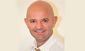
Wednesday, the longest day of the XVI B-MRS Meeting started with a plenary lecture on conjugated polyelectrolytes, a class of water-soluble polymers capable of conducting electricity and emitting light. This was one of the sessions that showed the relationship between the understanding of natural phenomena (fundamental research) and the development of social impact applications – which was the theme of the memorial lecture of the event. Professor Kirk Schanze (University of Texas at San Antonio) showed how detailed understanding of the mechanisms that underlie the properties of a material allows developing or improving products. Schanze and his team have in fact been conducting fundamental and applied research on conjugated polyelectrolytes, and have also generated a startup to market products derived from their laboratory work. In the lecture, the scientist presented some of his group’s work in the use of these materials as sensors of several ions and molecules that provoke or cancel their fluorescence. Processed as films, polyelectrolytes can also be used in organic photovoltaic cells to generate electricity from solar energy, Schanze said. At the end of the lecture, the professor demonstrated that these polymers can also be extremely useful in eliminating bacteria. In fact, particles covered with polyelectrolyte coatings have the ability to attract and adsorb bacteria in solution, besides emitting green light when the target has been seized. In his closing statement, Schanze, who is editor in chief of the renowned journal ACS Applied Materials and Interfaces, presented the newest associate editor of the journal, Professor Osvaldo Oliveira Jr (President of B-MRS!), and showed the papers of the most cited authors from Brazil in the journal (also members of B-MRS!).
In the afternoon, fog had already gone in Gramado, but not in the screen of the main room at the convention center. Professor Frédéric Guittard (Université Nice Sophia Antipolis, France) opened his speech with a photo of a narrow suspension bridge partially immersed in thick fog – a photographic summary of the scientific work, in which only one step can be taken at a time, the future is always uncertain, but it is necessary to go forward. The theme of the lecture, incidentally, also had to do with humidity. Guittard coordinates one of the leading groups in the world on wettability research, more precisely on hydro and oleophobic materials and their “super” versions. Some time ago, the French scientist said, in order to obtain materials of this type, researchers worked only with the chemical modification of surfaces, obtaining contact angles (angle between a drop of the liquid and the surface with which it came in contact) of 100 to 120 degrees for water and 40 degrees for oil. Currently, using a combination of physical and chemical methods, it is possible to produce “super-liquid-phobic” surfaces, which are those whose contact angle is greater than 150 degrees. These physico-chemical approaches contemplate surface roughness, porosity, topology and composition, among other factors, and considers both micro and nano levels. The inspiration for the scientific community to follow a more complex approach, Guittard said, came from biomimetics (the human quest to understand the strategies used by nature to reach the properties of plants and animals, and their scientific-technological application). “In nature, the macro, micro, nano and subnano scales communicate permanently,” exemplified the plenarist. In his particular case, the source of inspiration for developing superphobic surfaces was an artichoke planted to satisfy a desire of his children. The plant did not get wet while being watered. “I’ve rediscovered the Lotus effect,” Guittard said. From the fisrt steps at 40 degrees of contact angle to the present of over 150 degrees, the wettability area has generated a huge amount of papers, patents, production processes, books and review articles, said the scientist. Not only on the manufacture and characterization of surfaces with low wettability, but also, more recently, on the uses that can be made of them: antifreeze, anti-fog, self-cleaning, antiadhesion of bacteria, water harvesting and many others.
In the late afternoon, representatives from materials research societies / communities gathered in a room of the convention center to discuss ways to collaborate, from promoting student exchanges to encouraging greater participation of their communities in the events of the societies of other countries.
 Delegates of materials research societies/communities: from the left, Jorge Guerra (Peru), Francisco Rumiche (Peru), Daniel Weibel (chair of the event), Claudia Gutiérrez Wing (Mexico), Roberto Arce (Argentina), Soo Wohn Lee (IUMRS), Juliano Casagrande Denardin (Chile), Osvaldo Novais de Oliveira Junior (B-MRS), Guillermo Solórzano (B-MRS founder), Robert Chang (IUMRS) and Roberto Mendonça Faria (B-MRS and IUMRS).
And the longest day of the event lasted, in fact, until the next day. In fact, on Wednesday night, about 350 participants packed the Harley Motor Show, a themed bar and museum that honors the legendary motorcycle brand, to take part in the always-awaited “Conference Party”. Starting at 9:00 pm, groups settled down at the tables to drink, eat and enjoy the DJ’s varied musical repertoire, took pictures of the collection bikes that adorned the environment (lit and furnished in the style of Las Vegas casinos) and danced to the dawn. The party was sponsored by the journals ACS Applied Materials and Interfaces, ACS Nano, NanoLetters, Chemistry of Materials, JACS, Langmuir, ACS Central Science, ACS Energy Letters and ACS Omega.

The morning after the party, the last plenary of the event had, surprisingly, as much public as the previous ones. Why? Perhaps for starting a little bit later, at 10:45 am, and probably because of the interest in the speaker (one of the pioneers of nanotechnology, h index = 144) and in the subject (challenges and opportunities of nanoengineering). The first words of Professor Pulickel Ajayan (Rice University), which has research groups from Brazil among his collaborators, were in solidarity with the Brazilian scientific community regarding the financial problems. Then, the lecture began with a reference to biomimetics. From a photo of sea shells, Ajayan recalled that nature has always known how to do nanoengineering and that it uses the methods known as bottom-up – those that consist of joining or manipulating one by one the smallest bricks possible (atoms, molecules and even electrons) to construct functional structures. Throughout the plenary, the scientist shared several strategies and some secrets, based on solid results of fundamental research, on manufacturing functional nanomaterials. Ajayan, who pioneered the filling of a carbon nanotube 14 years ago, showed a series of nanomaterials (films, foams, nanoparticles, nanocomposites) through beautiful images of the nanoworld, accurately developed in his research group through various bottom-up methods. The scientist, who said he was very fond of basic science but confessed to be more excited when there is an application, also presented some of the devices he has created with his team and collaborators, mainly in the area of energy storage (batteries and supercapacitors), and companies that are marketing some of these innovations. Despite so many results from his nanoengineering strategies, Professor Ajayan said he believes that someday mankind will be able to develop better ways of producing nanomaterials – something that nature has already achieved.
Thursday. Students awards and closing cerimony.
After the lecture, the plenary room was transformed into a ceremony room to host the students awards ceremony, another tradition of B-MRS annual meetings, which this year had prizes bestowed by four different entities. Between palms and photographs, 20 students received awards for their work. B-MRS, represented by its president, gave the certificates of the “Bernhard Gross Award”, which honors by its name a pioneering scientist of materials research in Brazil. Among these finalists, five students received the awards from ACS Publications, whose certificates were delivered by Professor Kirk Schanze. These five award winners also won cash awards, sponsored by the American Chemical Society (ACS) journals ACS Applied Materials and Interfaces, ACS Nano, NanoLetters, Chemistry of Materials, JACS e ACS Omega.
Next, the four E-MRS award winners were announced for the best oral and poster of symposium K and three IUMRS poster award winners were also announced. The winners that were in the cerimony received the certificates in the hands of representatives of the two entities, respectively, Jeffrey Kettle and Soo Wohn Lee.
To conclude, the president of B-MRS and the chair of the event said some words. Both expressed their gratitude to all participants, organizing team, committees, students who help with the organization, symposia coordinators, plenarists, funding agencies, exhibitors, sponsors of the prizes and the party, host institution (UFRGS). Professor Novais de Oliveira also thanked Professor Weibel for being “a tremendous chair” and turned the “farewell” into “see you next year” by remembering that the next society meeting, the XVII B-MRS Meeting, will be held in Natal , capital of Rio Grande do Norte Brazilian state, from September 16 to 20, 2018.
![]() It is with great satisfaction that SBPMat announces the 17th edition of its annual event (XVII Meeting of SBPMat / B-MRS Meeting) to be held in the city of Natal (Rio Grande do Norte State), at the Convention Center of Hotel Praiamar, from September 16 to 20, 2018, under the coordination of Professor Antonio Eduardo Martinelli (Federal University of Rio Grande do Norte, UFRN).
It is with great satisfaction that SBPMat announces the 17th edition of its annual event (XVII Meeting of SBPMat / B-MRS Meeting) to be held in the city of Natal (Rio Grande do Norte State), at the Convention Center of Hotel Praiamar, from September 16 to 20, 2018, under the coordination of Professor Antonio Eduardo Martinelli (Federal University of Rio Grande do Norte, UFRN).
Save the date!
|
|||||||||||||||||||||||||||||||||||||||||||||||||||||
|
|||||||||||||||||||||||||||||||||||||||||||||||||||||
|
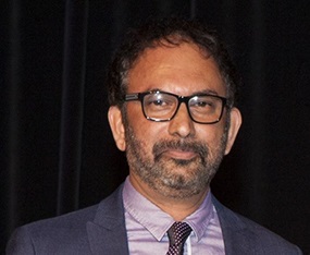
Despite all the knowledge on nanotechnology generated over the last few decades, applying nanomaterials to commercial products can still be a difficult task. At the XVI B-MRS Meeting, Professor Pulickel Ajayan, one of the world’s references in nanomaterials and nanostructures, will shed light on this problem. In the plenary lecture he will address in Gramado on the morning of September 14, Ajayan will discuss some challenges of the application of nanomaterials (particularly those of two dimensions) in systems and devices. He will address issues related to the synthesis, characterization and modification of these materials.
Ajayan and his collaborators have developed nanomaterials with diverse functionalities, applicable to fileds such as energy storage and conversion, catalysis, low consumption electronics, nanomedicine or environment care. Among his most famous contributions, are carbon nanotubes filled with molten material acting as nanowire moulds (1993); nanobrushes made of carbon nanotubes, highlighted by Guinness World Records as the smallest ones (2005); the paper battery, made of cellulose and nanotubes (2007); the ultra-dark nanotube carpet, which reflects only 0.045% of light (2008), and a reusable sponge of nanotubes capable of absorbing oil dispersed in water (2012).
Professor and director of the Department of Materials Science and Nanoengineering at Rice University (USA), Ajayan has exceptional publication metrics: a h index of 144 and more than 95,000 citations according to Google Scholar.
Pulickel Madhavapanicker Ajayan was born in 1962 in India, in a small town in the southern state of Kerala. He attended primary school there and then went to the state capital, to a high school that aroused his enthusiasm for learning, his curiosity, and his interest in science.
In 1985, Ajayan graduated in Metallurgical Engineering at Banaras Hindu University (BHU), located in northeastern India and then went on to do a PhD in Materials Science and Engineering at Northwestern University (USA). At that moment, he began to penetrate nanotechnology. In 1989, he defended his PhD thesis about very small gold particles that, some years later, would begin to be called “nanoparticles”.
In 1990, he moved to Japan to pursue a postdoctoral stage at the Fundamental Research Laboratory of the NEC Corporation, where he remained until 1993 in the group that was responsible for a series of seminal studies on carbon nanotubes – including the “discovery” of these nanomaterials, attributed to Sumio Iijima in 1991. During his postdoc, Ajayan obtained important results on the synthesis of nanotubes in large scale and on the filling of nanotubes with other materials.
From Japan, he went to France where he worked as a researcher at the Solid Physics Laboratory of the Université Paris-Sud for two years. Then he went to Germany, where he worked for a year and a half at the Max-Planck-Institut für Metallforschung. In 1997, he moved to the United States to become an assistant professor at the Rensselaer Polytechnic Institute (RPI), the nation’s oldest university of technological research, located in the state of New York. At RPI, he was the Henri Burlage chair Professor in Engineering and worked in the nanotechnology research group.
In 2007, he left RPI and joined the faculty of the Department of Mechanical Engineering and Materials Science at Rice University to be the Benjamin M. and Mary Greenwood Anderson professor of Engineering. In 2014, he also held the founding chair of the Department of Materials Science and NanoEngineering.
Currently, in addition to teaching and leading a research group of about 40 members at Rice University, Ajayan travels a lot, whether to share his knowledge on nanotechnology (he has delivered more than 350 invited lectures and has held visiting professor positions at universities around the world), or to take care of his scientific collaborations. In addition, Ajayan has acted on the boards of several journals, startups and international conferences of the materials and nanotechnology field.
The scientist has received important awards from a number of institutions including the Royal Society of Chemistry (UK), Alexander von Humboldt Foundation (Germany), Materials Research Society (USA), Microscopic Society of America (USA). He also received distinctions of numerous universities around the world, including the doctorate honoris causa by the Université Catholique de Louvain (Belgium). He is an elected member of the Royal Society of Chemistry (UK), American Association for the Advancement of Science (AAAS), and the National Academies of Sciences of India and Mexico, among other scientific societies.
Here follows an interview with the scientist.
B-MRS newsletter: – We would like you to choose some of your contributions to nanotechnology, describe them briefly, and share the paper reference, if possible. Please choose:
– The one(s) you consider to have caused or will cause more social impact.
Pulickel Ajayan: – Several of our discoveries have commercial and social impact. In the past two decades some of the research highlights from our lab have been carbon nanotube arrays as extreme light absorbers (for thermo-photovoltaics), nanotube arrays as gecko-tapes, high conductivity carbon nanotube fibers, graphene oxide membranes for water filtration, carbon nanomaterials for energy storage, light weight polymer nanocomposites, development of two-dimensional materials for electronics and sensors, carbon based quantum dots as catalysis for example CO2 reduction etc.
– The one(s) that gave you more personal satisfaction.
Pulickel Ajayan: – One of the most exciting work was related to the conversion of carbon onions into diamond nanoparticles using electron irradiation. This work was done in collaboration with Prof. Florian Banhart when I was visiting as a post-doc at the Max Planck Institute for Metallforschung in Stuttgart in the mid-90’s. This work published in Nature magazine showed direct observation of graphite to diamond phase transition without application of any external pressure.
B-MRS newsletter: – Have any of your scientific/ technological contributions been transferred to a commercial product? If so, has this transfer occurred through patent licensing, start-up …?
Pulickel Ajayan: – Two start-up companies (Paper Battery Co. and Big Delta Systems) have come out of our work; both engage in unconventional energy storage technologies.
B-MRS newsletter – Leave an invitation to your plenary talk for our readers.
Pulickel Ajayan: – Nanotechnology is a paradigm changing approach on how we will be building materials of the future. It is at the core of bottom-up manufacturing and will impact several areas of future technologies. Our work in the past two decades have focused on creating nano-engineered materials with various types of nanoscale building blocks.
More information
On XVI B-MRS Meeting website, click on the photo of Pulickel Ajayan and see his mini CV and the abstract of his plenary lecture: http://sbpmat.org.br/16controter/home/
Besides repelling water, superhydrophobic materials can be useful in a myriad of applications. Anti-ice, anti-corrosion and anti-bacterial systems, oil/water separation, water purification and desalination, and drug delivery are just a few examples. At the XVI B-MRS Meeting, this wide range of possibilities will be presented in a plenary lecture by Professor Frédéric Guittard.
Together with his research group at the University of Nice Sophia Antipolis (France), Guittard gets inspiration from nature to create hydrophobic and oleophobic surfaces based on conductive polymers and other materials. In these topics, the group has dozens of patents and articles (seven of them, highlighted in the covers of journals of Chemistry, Polymers and Materials since 2014), and is among the few most cited groups in the world.
Frédéric Guittard obtained his doctoral degree in Organic Chemistry in 1994 from the University of Nice Sophia Antipolis, and remained in the institution as a postdoc for about a year. Between 1995 and 1996, he carried out postdoctoral internships at institutions in the cities of Padua (Italy), Preston (United Kingdom) and Prague (Czech Republic). From 1996 to 1997, he worked in the pharmaceutical industry in the Principality of Monaco.
In 1997, he returned to his alma mater, the University of Nice Sophia Antipolis, as an associate professor, becoming a full professor in 2002. From 2004 to 2010, he was the director of the university’s Chemistry Department. Concerning laboratory leadership, Guittard coordinated the Laboratory of Chemistry of Organic and Metallic Materials and, since 2017, leads a new laboratory, the N.I.C.E. ®, whose name refers not only to its location in the city of Nice, but also to the acronym of “Nature Inspires Creativity Engineers”. In addition, Guittard created, and already directs, a professional master’s degree program in Materials and Management at the University of Nice.
In 2012, 2014 and 2016, Guittard was the chairman of the first editions of the international conference on materials inspired by nature, also identified with the trademark N.I.C.E.
Currently, Guittard is a visiting professor at University of California, Riverside (USA).
His scientific production, which has more than 5,200 citations, includes books, more than 230 articles and 35 patents.
Here follows an interview with the scientist
B-MRS Newsletter: – Your research has a biomimetic approach. In what elements of Nature do you take inspiration to develop your hydro and oleophobic materials?
Frédéric Guittard: – From an artichoke. My kids wanted me to grow an artichoke: when I watered it, surprisingly I rediscovered the Lotus effect. The next steps were to adapt, to adopt, to integrate this secret from Nature into technologies or biotechnologies.
B-MRS Newsletter: – In your opinion, what are your main scientific or technological contributions in the field of hydrophobic and oleophobic materials? Please describe them briefly, and share the paper reference, if possible.
Frédéric Guittard: – There are some interesting applications for superhydrophobic or superoleophobic materials. The main applications concern the anti-adhesion (like anti-graffiti, anti-icing, anti-fingerprints …) or anti-bioadhesion (like anti-fouling or for example to remove bacteria from surfaces in hospitals). The following publications will give more details:
– Bioinspired Superhydrophobic Surfaces: Advances and Applications with Metallic and Inorganic Materials, CRC Press, Francis & Taylor Group, 300 pages, 2017 (F. Guittard, T. Darmanin)
– Superhydrophobic and Superoleophobic Properties in Nature, Materials Today, 2015, 18, 273-285 (T. Darmanin, F. Guittard)
– Recent advances in the potential applications of bioinspired superhydrophobic materials, Journal of Materials Chemistry A, 2014, 2, 16319-16359 (T. Darmanin, F. Guittard)
B-MRS Newsletter: – Your laboratory has an extensive list of industrial partners. Is university-to-industry knowledge transfer common in your laboratory? If so, in what way does it happen? Via patent licensing, spin-offs, joint projects?
Frédéric Guittard: – The first point is to understand that Industries and Universities are not competitors but can form a chain of value. In this way, the industries have to innovate in order to improve or to create the service. The Universities can help the industries to show amazing solutions with a proof of concept. Even if the cost is important to take into account, the key point at 80% for success is the good human relationship. More often, the solution is near us and the effort is weak! We have to see and to observe in order to find the key parameter and to ask the question where is the best in class from all the phenomena in the world (not only in the same field). It is like the benchmarking approaches.
Patent, licensing, spin-offs or joint projects can be used according to the origin of the idea and its realization.
More information
On XVI B-MRS Meeting website, click on the photo of Frédéric Guittard and see his mini CV and the abstract of his plenary lecture: http://sbpmat.org.br/16controter/home/
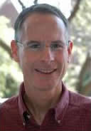
In the research group of Professor Kirk Schanze, conjugated polyelectrolytes (CPEs) have been the subject of both fundamental studies and applications. The group has already explore CPEs as fluorescent sensors, in solar cells and as biocidal materials.
On September 13, in Gramado, Kirk Schanze, who is a Professor at the University of Texas at San Antonio (UTSA) and editor-in-chief of ACS Applied Materials & Interfaces, will take some time out of his busy schedule to deliver a plenary lecture on CPEs in the XVI B-MRS Meeting.
Schanze graduated in Chemistry from Florida State University in 1979. Four years later, he earned his Ph.D., also in Chemistry, from the University of North Carolina at Chapel Hill. Soon after, he was appointed a Miller Postdoctoral Fellow at the University of California, Berkeley. In 1986, he joined the University of Florida (UF) as a professor of the Department of Chemistry. There, he chaired the Division of Organic Chemistry, held the Prominski Chair of Chemistry, and founded the Schanze Group, which today continues its research activities at UTSA. In 2016, Schanze left UF to hold the Robert A. Welch Distinguished University Chair in Chemistry at UTSA.
Between 2000 and 2008, Schanze served as senior editor of the prestigious journal Langmuir. Shortly thereafter, he became the first editor-in-chief of ACS Applied Materials & Interfaces, which had just been released.
Prof. Schanze has authored about 300 papers and 20 patents. According to Google Scholar, his scientific production has more than 16,000 citations and his h index is 71. He is fellow of the American Chemical Society (ACS). He was a visiting professor at the Harbin Institute of Technology (China) and the Tokyo Metropolitan University (Japan) in 2011, at the Ecole Normale Supérieure Cachan (France) in 2008 and at the Chemical Research Promotion Center (Taiwan) in 2007. He has received distinctions from the American Chemical Society, National Science Foundation, University of Florida, Japan Society for Promotion of Science, and Japanese Photochemical Association, among other entities.
Here follows an interview with the scientist.
B-MRS newsletter: – In your opinion, what are your main scientific and/ or technological contributions to the field of conjugated polyelectrolytes? Describe them briefly and feel free to share a few references of your papers, patents or books.
Kirk Schanze: – We were among the first groups to study conjugated polyelectrolytes, which are water soluble conjugated polymers. Following are some of the key contributions from our group to this field:
a) Our lab was the first to report the synthesis of a water soluble, fluorescent poly(phenylene ethynylene) sulfonate (PPE-SO3) and describe the application to fluorescence sensing of ions in water at ultralow concentration.[1]
b) We were the first to report the use of a fluorescent conjugated polyelectrolyte as a sensor for enzyme activity, which is an important biosensing application.[2]
c) Our lab has developed the applications of cationic conjugated polyelectrolytes to sensing phosphatase enzyme activity. These enzymes are important in a number of biologically significant processes. [3,4]
d) Working in collaboration with Prof. David Whitten of the University of New Mexico, we have developed cationic conjugated polyelectrolytes as a novel class of antibacterial agents.[5,6]
References:
[1] C. Tan, M. R. Pinto and K. S. Schanze, “Photophysics, Aggregation and Amplified Quenching of a Water-Soluble poly(Phenylene ethynylene)”, Chem. Commun. 2002, 446-447, 10.1039/B109630C.
[2] M. R. Pinto and K. S. Schanze, “Amplified Fluorescence Sensing of Protease Activity with Conjugated Polyelectrolytes”, Proc. Nat. Acad. Sci. USA, 2004, 101, 7505, 10.1073/pnas.0402280101.
[3] Zhao, X.; Liu, Y.; Schanze, K. S., “A Conjugated Polyelectrolyte Based Fluorescence Sensor for Pyrophosphate”, Chem. Commun. 2007, 2914-2916, 10.1039/b706629e.
[4] Zhao, X. Y.; Schanze, K. S., “Fluorescent Ratiometric Sensing of Pyrophosphate via Induced Aggregation of a Conjugated Polyelectrolyte”, Chem. Commun. 2010, 46, 6075-6077, 10.1039/c0cc01332c.
[5] Ji, E.; Corbitt, T. S.; Parthasarathy, A.; Schanze, K. S.; Whitten, D. G., “Light and Dark-Activated Biocidal Activity of Conjugated Polyelectrolytes”, ACS Appl. Mater. Interfaces 2011, 3, 2820-2829, 10.1021/am200644g.
[6] 299. Huang, Y.; Pappas, H. C.; Zhang, L.; Wang, S.; Cai, R.; Tan, W.; Wang, S.; Whitten, D. G.; Schanze, K. S., “Selective Imaging and Inactivation of Bacteria over Mammalian Cells by Imidazolium Substituted Polythiophene”, Chem. Mater. 2017, 2017, 29, 6389–6395, 10.1021/acs.chemmater.7b01796.
B-MRS Newsletter: – You have been the Editor-in-Chief of ACS Applied Materials & Interfaces since its release, haven´t you? In less than 10 years, the journal hit an impact factor of 7,504. To what factors do you attribute this good result?
Kirk Schanze: – ACS Applied Materials & Interfaces (AMI) publishes papers that come from a currently very active area of materials research, specifically applied materials/interfaces. There is a large community of scientists and engineers around the globe who are working in this field. AMI has a global community of editors and editorial board members who represent their regions. Indeed, the newest editor who has joined our editorial board is Prof. Osvaldo Oliveira Jr. of the University of Sao Paulo!
B-MRS Newsletter: – We often see papers from the Brazilian Materials Community at ACS Applied Materials & Interfaces. Could you share with our readers some numbers about the participation of Brazilian authors in the journal?
Kirk Schanze: – ACS Applied Materials & Interfaces has published more than 100 papers with authors or co-authors from Brazil. Many of these papers have been highly cited in the field of materials science. Examples of highly cited papers are:
B-MRS Newsletter: – Please, leave an invitation to your plenary talk.
Kirk Schanze: – Everyone is invited to attend my talk which will highlight our work of conjugated polyelectrolyte as applied in the field of energy- and bio- materials chemistry.
More information
On XVI B-MRS Meeting website, click on the photo of Kirk Schanze and see his mini CV and the abstract of his plenary lecture: http://sbpmat.org.br/16controter/home/
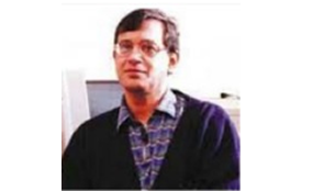
In the race to develop ever smaller and better performing chips, several technological limitations need to be overcome. Today, the bottlenecks to continue this trend lie mainly in techniques for manufacturing electronic circuits of less than 10 nanometers (nm). Among the techniques being improved to manufacture the next generation of chips, one of the most promising is extreme ultraviolet lithography (EUVL). This technology takes advantage of the very short wavelength of extreme ultraviolet radiation to pattern nanoscale circuits on the chip with the intermediation of the so-called “resists” – thin layers of radiation sensitive material that cover the chip substrate during nanofabrication.
At the XVI B-MRS Meeting, a plenary lecture will discuss an important contribution that the materials field can make to the next generation of chips: the development of suitable resists for the fabrication of electronic circuits of less than 10 nm through EUVL.
The subject will be presented by Kenneth E. Gonsalves, Distinguished Professor of the Indian Institute of Technology Mandi (IIT Mandi), a teaching and research institution created in 2009, where Gonsalves arrived in 2012 as a visiting professor.
Gonsalves obtained his BS in Chemistry from the University of Delhi (India) followed by an MS also in Chemistry from Boston College (USA) and a PhD from the University of Massachusetts at Amherst (USA) with a doctoral thesis on polymer synthesis. Then he performed a postdoctoral specialization on polymer ceramics at MIT (USA). From 2001 to 2014, Gonsalves was the Celanese Acetate Distinguished Professor of Polymer Materials at the University of North Carolina at Charlotte (USA).
Together with his research group at IIT and his collaborators from the United States, India, Brazil, Taiwan and Europe, Gonsalves carries out research and development on resists for advanced nanofabrication techniques, with support of major companies in the electronics segment, and on polymer scaffolds for tissue engineering.
Here follows a brief interview with the researcher.
B-MRS newsletter: – Tell us a little bit about your main scientific/ technological contributions up to the moment.
Kenneth Gonsalves: – My research has centered on polymers with an emphasis on synthesis of novel materials. For the last 20 years I have focused on resist technology for IC (integrated circuit) fab. This is a fascinating area as it has significant technological applications in the development of integrated circuits, solid state devices. In addition it can also be used successfully for cell and tissue engineering of scaffolds for biotechnologies.
B-MRS newsletter: – About the resists you are working on, what skills and expertise are needed to develop them, in your opinion? When this next generation of chips is expected to be available?
Kenneth Gonsalves: – Resist R&D is multifaceted and extremely complex. It requires extensive collaborations between chemists with organic, inorganic and polymer backgrounds. In addition, interaction with physicists and electrical/electronic engineers is essential. The next generation of chips at the 14 nm node are currently available. Sub 7 nm node technology is expected by 2018 onwards.
B-MRS newsletter: – Describe in the simplest and briefest possible way the process of EUVL, without forgetting to mention the role of resists.
Kenneth Gonsalves: – The EUV photons are generated by a plasma or synchrotron source operating at a wavelength of 13.5 nm. Through a series of special mirrors and a mask, the predesigned template for the IC fab is projected onto photosensitive materials such as polymers as well as inorganics. This is all conducted in vacuum, a challenge for the IC fab industry as it is a drastic change from current photolithography fab, which functions under ambient conditions. The extremely short EUV wavelength is a prerequisite for patterning features at the sub 20 nm scale. The challenges for resists that can meet the sub 7 nm node requirements are enormous. A new paradigm is paramount – hybrid resists, that are partially inorganic may provide solutions to patterning at these scales. Inorganic hardmasks are another alternative. The sensitivity of these photoresists has to be enhanced drastically in order to meet the mass volume production of chips. There are several other critical parameters that have to be met for a successful resist system. Again, this requires multidisciplinary, multi institutional, industry collaboration on a global scale.
——————
More information
On XVI B-MRS Meeting website, click on the photo of Kenneth Gonsalves and see his mini CV and the abstract of his plenary lecture: http://sbpmat.org.br/16encontro/home/