
|
||||||||||||||||
|
||||||||||||||||
|
|
||||||||||||||||
|
||||||||||||||||
|
|
|||||||||||||||||||||||||||||
|
|||||||||||||||||||||||||||||
|
[Exploring Au Droplet Motion in Nanowire Growth: A Simple Route toward Asymmetric GaP Morphologies. Bruno C. da Silva*, Douglas S. Oliveira, Fernando Iikawa, Odilon D. D. Couto Jr., Jefferson Bettini, Luiz F. Zagonel, and Mônica A. Cotta*. Nano Lett., 2017, 17 (12), pp 7274–7282. DOI: 10.1021/acs.nanolett.7b02770]
Moving nanoparticles for asymmetric nanowires.
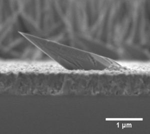
A team of scientists presented a route to grow semiconductor nanowires having an asymmetric morphology, different from the traditional cylindrical one. The possibility of producing, in a controlled manner, nanowires with particular formats and without defects, can be exploited in several applications, including the production of more efficient solar cells.
The research was led by scientists from the Brazilian university UNICAMP and the Brazilian Nanotechnology National Laboratory (LNNANO), who reported their findings in a paper in NanoLetters.
The researchers discovered the process while studying the production of nanowires of gallium phosphide (GaP) for optoelectronic applications. The team chose to produce the nanowires by chemical beam epitaxy (CBE), preceded by a thermal treatment (annealing). In this technique, a substrate of a suitable material – in this case gallium arsenide (GaAs) – is placed inside a chamber. Then, chemical compounds in the form of vapor are introduced into the chamber. Some elements of the vapored material deposit over the substrate, layer upon layer, generating films. To promote the growth of nanowires instead of films, metallic nanoparticles (in this case, gold nanoparticles) are placed on the substrate before being exposed to vapor. During exposure, these catalytic nanoparticles cause the material to deposit preferentially underneath them, causing wire-like structures to grow.
While the researchers were analyzing the nanowires they had obtained in the first few months of the work, they found a significant amount of asymmetric nanostructures. “Besides having a particular morphology, we saw that these nanowires had an hexagonal crystal structure (wurtzite) and a very low density of crystallographic defects, which motivated us to study in detail the causes for the formation of this unusual structure,” says Bruno da Silva, PhD student at UNICAMP and corresponding author of the paper.
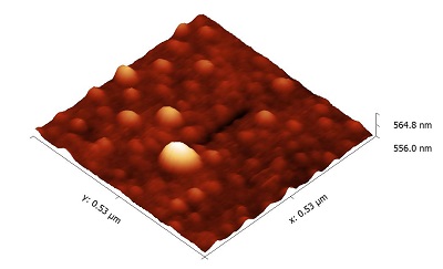
Da Silva and his supervisor Prof. Mônica Cotta then began to raise and test hypotheses for the cause behind the formation of the peculiar structures. After several experiments and analyses, they focused on a phenomenon that caught their attention: in the early stages of the process, the gold nanoparticles spontaneously moved over the substrate. Hence, the duo undertook a systematic work on heating substrates with nanoparticle catalysts, growing nanowires under various conditions, and analyzing the resulting samples through scanning and transmission electron microscopes and atomic force microscopy.
Da Silva, Prof. Cotta and their collaborators from UNICAMP and LNNano were able to find out why the growth process they used resulted in asymmetric nanowires. The main reason was the movement of the gold nanoparticles, which was thermally activated with the initial annealing. Based on that discovery, the team established a recipe for producing asymmetric semiconductor nanowires in a controlled manner. “Our work was the first to show that the mechanical instability of the nanoparticle catalyst can be used to modify the growth of semiconductor nanowires, in our case, particularly affecting their morphology,” says Bruno da Silva.
The mechanism of the asymmetric nanowires growth presented in the NanoLetters paper can be described as follow. When heated together with the substrate, the nanoparticles begin to crawl and advance through the substrate while consuming the oxide layer that naturally covers the gallium arsenide. Thus, the nanoparticles form asymmetric grooves a few nanometers deep and a few hundred nanometers long. These trails become fertile ground for the growth of the nanowires, since the deposition rate of the vapored material is greater there than in the rest of the substrate, which is covered by the oxide. A pedestal then forms along the grooves and the nanowire grows on top of the pedestal with an asymmetrical format. “We showed that the movement of the particle generates a zone of preferential deposition, and that the combination of this phenomenon with the axial growth “vapor – liquid – solid” leads to the asymmetry in the nanowire,” summarizes da Silva.
Besides describing the formation mechanism of asymmetric nanowires, the work of the Brazilian team generated detailed knowledge about the movement of heated metallic nanoparticles. “We have shown that in addition to temperature, vacuum conditions and surface quality of the substrate are crucial for nanoparticle stability, and that the motion direction is related to the asymmetry of gold dissolution on semiconductor surfaces III-V,” details the doctorate student.
Concerning possible applications, the asymmetry of these nanowires can be explored, for example, in the construction of antireflective layers that reduce the amount of light lost by reflection in solar cells. Another possibility would be to exploit the green emission of these wurtzite gallium phosphide nanowire in lighting devices. Or, why not, to develop an alternative process to electronic litography taking advantage of the gold nanoparticles movement and the trails it forms on the substrate.
The work was funded by Unicamp, the Brazilian federal agencies CNPq and CAPES and the São Paulo Research Foundation (FAPESP).
Reelected in January of this year, Professor Osvaldo Novais de Oliveira Junior (IFSC-USP) began his second consecutive mandate as president of the Brazilian Materials Research Society (B-MRS) this February, together with a partially renewed board of directors, composed of Professor Rubem Luis Sommer (CBPF) in the administration, finance and equity sector, and as scientific directors, Professors Antonio Eduardo Martinelli (UFRN), Daniel Eduardo Weibel (UFRGS), Glaura Goulart Silva (UFMG), Iêda Maria Garcia dos Santos (UFPB) and Mônica Alonso Cotta (Unicamp). This board will manage the society for two years until the end of 2019.
Currently, Professor Novais de Oliveira Junior (or “Chu”, as he is known) is a full professor at the São Carlos Institute of Physics – University of São Paulo (IFSC-USP) and associate editor of the journal ACS Applied Materials & Interfaces. With an H index of 58, his name is among the 100 scientists in Brazil of all areas with higher H index. He is author of about 500 articles and his works include nearly 15,500 citations (Google Scholar data).
In this interview, the re-elected president speaks a little about his first term in B-MRS, the management he will initiate in this new mandate and his current scientific activities.
B-MRS Newsletter: You have just completed your first term as president of B-MRS. Share with our readers your thoughts about the results achieved by the board you presided over.
Osvaldo Novais de Oliveira Junior: In the last mandate the board’s priority was to keep the Annual Meetings at a high level, despite the financial crisis Brazil’s science, technology and innovation system is undergoing. In addition to this priority, we continued the endeavors of previous boards in the internationalization of SBPMat, which include partnerships with scientific societies from other countries.
B-MRS Newsletter: – You have just accepted a new two-year term as president of SBPMat. Comment on your plans and expectations.
Osvaldo Novais de Oliveira Junior: The expectations of the Board of Directors are to be able to continue the activities that made SBPMat one of the most active and prestigious scientific societies in Brazil. The main plans I want to highlight concern working toward a greater insertion in the society, with the task of disseminating the contributions of science and technology to the country, and to increase the number of B-MRS members.
B-MRS Newsletter: About your scientific research work, share with us what you are doing.
Osvaldo Novais de Oliveira Junior: My group`s research work, in partnership with other groups in Brazil and abroad, focuses on two areas: i) the study and use of materials for biology and medicine, for example using biosensors for early diagnosis of cancer and determination of mechanisms at the molecular level of drugs to combat super-resistant bacteria. ii) the use of statistical physics methodologies and complex networks for text analysis, such as authorship identification of books and verification of multidisciplinarity in the scientific literature.
B-MRS Newsletter: If you wish, use this space to leave a message for the B-MRS members and the community that follows the news of this newsletter.
Osvaldo Novais de Oliveira Junior: I and the new board hope to have the enthusiastic support of the community, as in recent years.
Learn more about the trajectory of our president (interview of January 2016).
Prof Denis Chaumont is looking for a candidate for a PhD subject with funding (3 years by the French Ministry of Education), starting in September 2018.
Title of the project: Growth of hybrid TiO2 nanostructures under MOCVD for applications in energy field.
The candidate must be graduated Master M2 (BAC + 5) before September 1, 2018. The candidate must be a good candidate. The couple candidate/subject will be examined by a jury that will evaluate the ”quality” of the couple.
Interested candidates can send the following documents to Prof Chaumont (denis.chaumont@u-bourgogne.fr):
– a CV,
– a letter of motivation,
– the transcripts of the results and ranking of the year of Master M1,
– the opinion of the internship tutor of M1,
– the transcripts of the results and ranking of the first semester of the year of Master M2,
– a letter of recommendation …
Contact :
Denis CHAUMONT (MCF-HDR)
Nanoform, Laboratoire Interdisciplinaire Carnot de Bourgogne ICB
(UMR 6303 CNRS – Université de Bourgogne)
9, Avenue Alain Savary
BP 47 870, 21 078 Dijon Cedex, France
Phone: (33) 3 80 39 59 08 ; Fax : (33) 3 80 39 61 32
E-mail: denis.chaumont@u-bourgogne.fr
Website: http://icb.u-bourgogne.fr/fr/membres/132-permanents/enseignants-chercheurs/516-denis-chaumont.html or www.nanoform.fr
|
|||||||||||||||
|
|||||||||||||||
|
|
||||||||||||||||||||||||||||||||
|
||||||||||||||||||||||||||||||||
|