Featured paper: How to make more stable perovskite nanocrystals for more efficient LEDs.

Paper: Amine-Free Synthesis of Cesium Lead Halide Perovskite Quantum Dots for Efficient Light-Emitting Diodes. Emre Yassitepe, Zhenyu Yang, Oleksandr Voznyy, Younghoon Kim, Grant Walters, Juan Andres Castañeda, Pongsakorn Kanjanaboos, Mingjian Yuan, Xiwen Gong, Fengjia Fan, Jun Pan, Sjoerd Hoogland, Riccardo Comin, Osman M. Bakr, Lazaro A. Padilha, Ana F. Nogueira, and Edward H. Sargent. Adv. Funct. Mater. 2016. DOI: 10.1002/adfm.201604580.

How to make more stable perovskite nanocrystals for more efficient LEDs.

Nesta imagem ilustrativa, enviada por Emre Yassitepe, pontos quânticos azuis, verdes e vermelhos excitados por radiação ultravioleta exibem uma brilhante luminescência.
In this illustrative image, sent by Emre Yassitepe, blue, green and red quantum dots excited by ultraviolet radiation exhibit a brilliant luminescence.

Perovskite quantum dots have been seen as great candidates to compose a next generation of displays and lighting devices. In fact, these luminescent nanoparticles are able to emit high brightness light and very vivid and pure colors when receiving external energy. But the technological use of perovskite quantum dots still runs into some limitations, mainly linked to their instability, for these tiny particles can quickly react with the medium, agglomerate or increase in size, for example.

A team of scientists from institutions in Canada, Brazil and Saudi Arabia has found a solution to one of the problems limiting the advance of research and development in the field, the degradation of perovskite quantum dots during their synthesis. The study was reported in an article recently published in the journal Advanced Functional Materials (impact factor: 11.38).

The manufacture of perovskite quantum dots is traditionally carried out by placing in a flask a solution with a series of compounds which react among them and generate perovskite nanoparticles coated (passivated) with oleic acid (C18H34O2) and oleylamine (C18H35NH2).

The team performed experiments and computational simulations to understand how the formation of perovskite quantum dots occurred step by step and thus formulate a manufacturing method that would avoid the problem of degradation. The scientists realized that the key to the solution was to reformulate the “ingredients” of the process in order to remove the oleylamine that eventually created the conditions for the degradation of the quantum dots, which precipitated to the bottom of the flask.

“We focused on developing the new synthetic technique to passivate perovskite quantum dots with oleic acid,” says Emre Yassitepe, postdoc at the Nanotechnology and Solar Energy Laboratory of the Institute of Chemistry of Unicamp, who signs the article as the first author. “Oleic acid is one of the most common ligands to date to stabilize the quantum dots and we wanted to see the impact on stabilization and LED performance between different ligands.”

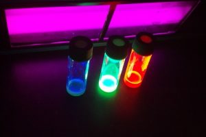
Following the new “recipe”, the team was able to produce quantum dots of about 8 nm, coated only with oleic acid, made of cesium, lead and elements of the group of halogens and having perovskite structure (which is a certain organization of the atoms). Green quantum dots (CsPbBr3), blue (CsPb (Br, Cl) 3) and red (CsPb (Br, I) 3) were produced and characterized.

One of the main gains achieved with the new method was the colloidal stability of the quantum dots: they remained intact more than oleylamine capped perovskite quantum dots after the purification step, which removes from the nanocrystals the residual compounds that usually remain from the manufacturing process.

The team went beyond the manufacturing and experimental analysis of quantum dots and built with them LED devices (light-emitting diodes, now widely used in lamps and displays) emitting green, blue and red light, in order to check their efficiency. They made thin films with the obtained perovskite quantum dots and placed a layer of this material “sandwiched” between a layer of titanium dioxide, in charge of transporting electrons (carriers of negative charge) and a polymer layer, destined to transport the so-called “holes” (positive charge carriers). In this LED, when applying an electric field, electrons and holes move to the quantum dots layer and excite them, causing them to emit photons and thus generate the desired light.

The use of polymer transport layers processed from solution instead of layers processed from evaporation to make perovskite LEDs was also an innovation made possible by the new “recipe”, which made quantum dots more robust against this type of processing.

As a final result, the team of scientists achieved bright and efficient blue and green LEDs. Perovskite LEDs made with oleylamine-free quantum dots demonstrated better performance in some respects than conventional perovskite LEDs produced with oleylamine coated quantum dots.

Pictures from the authors of the paper from Brazilian institutions. From the left: Ana Flávia Nogueira and Emre Yassitepe (Institute of Chemistry, Unicamp), Juan Andrés Castañeda and Lázaro Padilha (Institute of Physics, Unicamp).

“We have demonstrated a new synthetic method that enhances the colloidal stability of perovskite quantum dots by capping them solely by oleic acid”, summarizes Yassitepe. “The enhancement of stability of oleic acid capped perovskite quantum dots allows us to remove excess organic content in thin films. The excess inorganic content acts as an insulator between quantum dots reducing performance. By reducing the excessive ligands we are able to make more efficient and solution-processed perovskite quantum dot light emitting diodes” concludes the postdoc.

The work was funded by Canadian agencies, FAPESP (São Paulo State Research Foundation) and King Abdullah University of Science and Technology (Saudi Arabia). The experiments of transient ultra-fast absorption and analysis by transmission electron microscopy were carried out at Unicamp to characterize the quantum dots. The synthesis of the nanocrystals and the manufacture of LEDs were carried out at the University of Toronto in the group of Professor Edward H. Sargent, where Yassitepe performed a one-year internship during within his post-doc at Unicamp. “I am grateful to FAPESP- Bolsa Estágio de Pesquisa no Exterior project for giving me this opportunity,” says Yassitepe.

Featured paper: Changing the properties and morphology of graphene nanoribbons with nitrogen.

The scientific paper by members of the Brazilian community in Materials research featured this month is:

Josue Ortiz-Medina,  M. Luisa García-Betancourt,  Xiaoting Jia,  Rafael Martínez-Gordillo,  Miguel A. Pelagio-Flores,  David Swanson,  Ana Laura Elías,  Humberto R. Gutiérrez,  Eduardo Gracia-Espino,  Vincent Meunier, Jonathan Owens,  Bobby G. Sumpter, Eduardo Cruz-Silva,  Fernando J. Rodríguez-Macías,  Florentino López-Urías,  Emilio Muñoz-Sandoval, Mildred S. Dresselhaus,  Humberto Terrones,  Mauricio Terrones. Nitrogen-Doped Graphitic Nanoribbons: Synthesis, Characterization and Transport. Advanced Functional Materials 2013, 23, 3755-3762. DOI 10.1002/adfm.201202947.

Changing the properties and morphology of graphene nanoribbons with nitrogen

Multiple layers of graphene with the shape of ribbons (narrow and long) are called graphitic nanoribbons. These materials have been studied to control their properties by various methods, such as doping, in which are introduced atoms of “foreign” elements in the graphene carbon lattice.

In a study led by scientists at Pennsylvania State University with the participation of researchers from institutions in the United States, Mexico, Spain and Brazil, nitrogen-doped graphitic nanoribbons were manufactured by the chemical vapor deposition (CVD) method and showed new features, linked with the introduction of nitrogen, such as highest semiconductor performance, promising for applications in electronic devices, chemical reactivity and a very particular morphology on its edges.  The research was published in the journal Advanced Functional Materials.

“This article showed by the first time that it is possible to make doping with nitrogen on the same synthesis by CVD of graphite nanoribbons, and that you can control the level of doping during synthesis,” highlights Fernando Rodríguez-Macías, foreign visiting professor at the Brazilian Federal University of Pernambuco (UFPE) and one of the authors of the scientific paper. A Mexican national, Rodríguez-Macías came to UFPE in 2012, during his sabbatical year to work as a foreign visiting professor in the Department of Fundamental Chemistry and in the Graduate Program in Materials Science of the University. “I have prolonged my stay for another year to continue until 2014 doing collaborative studies for the production of carbon nanostructures, of bionanotechnology and toxicity of nanomaterials,” says the professor. “I am also teaching preparation and characterization of materials,” he adds.

The doped nanoribbons

The article’s authors showed that different concentrations of nitrogen generate controlled changes in material behavior. In particular, scientists have proven that the more nitrogen introduced into the structure of graphene, the most predominant the semiconductor behavior of nanoribbons. As an explanation to this phenomenon, the researchers suggested, based on theoretical calculations, that nitrogen atoms of doped nanoribbons act as scattering centers of electrons and decrease the conductive behavior of undoped graphene. “The control of doping level allows you to change the electrical properties of the nanoribbons, which can be useful for applications in transistors and other electronic devices,” says Rodríguez-Macías.

In addition, the paper also shows that the reactivity of nanoribbons can change with the doping level. Pure graphene, explains UFPE’s visiting professor, is very inert and has limited interactions with many chemical substances; on the other hand, nanoribbons doped with nitrogen are more reactive, which makes them useful for applications in sensors and catalysis.

As to the morphology, the article’s authors found that the nitrogen-doped nanoribbons have loops on their edges, uniting different graphene sheets. “This morphology is not presented by undoped graphite nanoribbons,” says Rodríguez-Macías.

This figure, sent by Professor Fernando Rodríguez-Macías, shows the nitrogen-doped graphitic nanoribbons in three scales. The scanning electron microscopy (top left corner) shows how these ribbons are made up of several layers and feature a curved surface with roughness. The transmission electronic microscopy (bottom left corner) shows that the nanoribbon layers are graphene sheets. The high resolution transmission electronic microscopy (right) shows that the layers of graphene on the nanoribbons edges form loops uniting different graphene sheets.

Collaborators

Almost all work of materials synthesis of the paper of Advanced Functional Materials was developed at Pennsylvania State University; the characterization was done in collaboration with other researchers and laboratories, reports UFPE’s visiting professor.

The participation of UFPE in the article happened through the doctoral student Miguel Angel Pelagio-Flores in the analysis and theoretical modeling of doped nanoribbons, and through professor Fernández-Macías himself, who, in addition to having participated in the discussion of results and review of the article from his office at UFPE, was doctoral advisor of the first author of the article, Josué Ortiz-Medina, while professor of a Mexican institution, IPICYT. “Ortiz-Medina did most of the experimental work of the article, besides being an important part of the characterization and theoretical studies of these new nanomaterials, when he was in exchange at Penn State in the laboratory of professor Terrones,” contextualizes the professor.

In total, 19 authors sign the article, among them MIT’s Professor Mildred Dresselhaus, reference in carbon science.

Artigo científico em destaque: Interação entre ouro e eumelanina – um material promissor para o desenvolvimento de dispositivos bioeletrônicos.

O artigo científico de membros da comunidade brasileira de pesquisa em Materiais em destaque neste mês é:

Julia Wünsche, Luis Cardenas, Federico Rosei, Fabio Cicoira, Reynald Gauvin, Carlos F. O. Graeff, Suzie Poulin, Alessandro Pezzella, Clara Santato. In Situ Formation of Dendrites in Eumelanin Thin Films between Gold Electrodes.  Advanced Functional Materials, 2013. Article first published online : 10 JUN 2013, DOI: 10.1002/adfm.201300715.

Texto de divulgação:

Interação entre ouro e eumelanina – um material promissor para o desenvolvimento de dispositivos bioeletrônicos

Olhos e ouvidos artificiais e dispositivos que realizem a interface entre o corpo humano e braços robóticos são algumas das aplicações que a Bioeletrônica promete. Ainda em estágio inicial, o desenvolvimento dessa área da pesquisa depende em boa parte do desenvolvimento de materiais que sejam semicondutores e biocompatíveis ao mesmo tempo. Um dos materiais mais promissores e mais estudados no contexto da Bioeletrônica é a eumelanina (um tipo de melanina determinante, por exemplo, na definição da cor dos cabelos dos seres humanos). A eumelanina começou a ser estudada sob a perspectiva da Ciência de Materiais na década de 1960, quando suas características semicondutoras foram descobertas. O problema é que a melanina, tanto a natural quanto a sintetizada por métodos tradicionais, não produz filmes finos de boa qualidade que viabilizem seu uso como material para dispositivos bioeletrônicos.

No ano 2004, no Brasil, mais precisamente na cidade de Ribeirão Preto (SP), na Universidade de São Paulo (USP), o grupo de pesquisa do professor Carlos Graeff desenvolveu uma forma de produzir melanina solúvel em dimetilsulfóxido (DMSO), o que possibilitou a produção de filmes finos de alta qualidade. A descoberta foi publicada no Journal of Non-Crystalline Solids (http://dx.doi.org/10.1016/j.jnoncrysol.2004.03.058). “A partir desta publicação e outras subsequentes recebemos o contato da professora Clara Santato, uma especialista na produção de dispositivos eletrônicos orgânicos da Escola Politécnica de Montréal (Canadá), para desenvolvermos um projeto comum”, relata o professor Graeff, atualmente professor da Universidade Estadual Paulista (Unesp) – campus de Bauru.

A colaboração então iniciada continuou ao longo dos anos e gerou uma pesquisa que demonstrou a existência de peculiares interações entre a eumelanina e o ouro. Os resultados desse trabalho foram publicados online no dia 10 de junho deste ano na prestigiada revista Advanced Functional Materials. O artigo agregou as competências em síntese de DMSO-melanina do professor Graeff, os recursos humanos e materiais para produção e caracterização de dispositivos eletrônicos a base de melanina do grupo da professora Santato e contribuições de outros grupos do Canadá e da Itália.

Dendritos
Dispositivos bioeletrônicos a base de filmes de eumelanina precisam, a princípio, de eletrodos para gerar uma corrente elétrica que flua através da eumelanina. Pensando nisso, os autores do artigo construíram um sistema composto por um substrato de dióxido de silício (SiO2) texturizado com partículas de ouro (os eletrodos) e, entre duas partículas do metal, depositaram o filme de eumelanina. Num contexto de 90% de umidade do ar e temperatura ambiente, aplicaram uma tensão de 1 volt, gerando um eletrodo positivo e outro negativo nas partículas de ouro e um fluxo de corrente elétrica entre elas.

Com o auxílio de um microscópio de força atômica, o experimento permitiu a observação de uma paulatina formação de nanoestruturas sobre o filme. Inicialmente, essas nanoestruturas surgiram próximas ao eletrodo positivo em forma de nanoagregados, compostos basicamente por ouro e por algo de eumelanina. Ao aplicar tensão por mais alguns minutos, novos nanoagregados foram surgindo e se aproximando do eletrodo negativo, até chegar a ele. Nesse momento, começou a nucleação dos nanoagregados, a qual gerou estruturas em forma de dendritos (as ramificações dos neurônios) com alto conteúdo de ouro, surgidas a partir da região de contato com o eletrodo negativo. Enquanto a tensão continuou a ser aplicada, os dendritos continuaram a se formar, chegando a unir o eletrodo negativo ao positivo por meio de suas ramificações.

Além de terem formato parecido, as nanoestruturas dendríticas e os dendritos neuronais se assemelham no papel que desempenham, o de transmitir impulsos elétricos. De fato, os dendritos crescidos no filme de eumelanina demonstraram ser altamente condutores.

Esta imagem de microscopia de força atômica mostra o filme de DMSO-eumelanina hidratado, de 30 nm de espessura, após receber tensão de 1 V durante 3 horas:

A imagem permite ver que os nanoagregados de ouro e eumelanina se formam na região próxima ao eletrodo positivo, avançam pelo filme e se depositam nas proximidades do eletrodo negativo, levando, finalmente, à formação dos dendritos.