
Sorry, this entry is only available in Brazilian Portuguese.
Author: Verónica Savignano
Members of B-MRS are authors of a new book on Density Functional Theory.
The members of B-MRS Sérgio Ricardo de Lázaro (UEPG professor) and Luis Henrique da Silveira Lacerda (PhD student at UEL/UEPG/UNICENTRO) are the authors of the book “Teoria do Funcional da Densidade e Propriedades dos Materiais“, published by the Brazilian publishing house CRV. The book is co-authored by Renan Augusto Pontes Ribeiro, also a doctoral student of the program. The Density Functional Theory (DFT) is based on Quantum Mechanics and was applied in the area of Materials Chemistry.
More information about the book: https://editoracrv.com.br/produtos/detalhes/33536-crv
B-MRS Member is editor of Elsevier’s new book on photonic nanostructures.
Professor Luciana Reyes Pires Kassab (School of Technology of São Paulo, Fatec São Paulo), member of B-MRS, is co-editor of the book “Metal Nanostructures for Photonics”. Published by the Elsevier publishing house, the book discusses the photonic properties and applications of metallic nanostructures, as well as the preparation and characterization techniques of these materials. Professor Luciana R. Pires Kassab edited the book with Professor Cid Bartolomeu de Araujo (UFPE). More than 40 authors from different countries sign the book’s 12 chapters.
More information about the book: https://www.elsevier.com/books/metal-nanostructures-for-photonics/pires-kassab/978-0-08-102378-5
Three PD positions available for glass research.
Applications for postdoctoral fellowships are invited for conducting fundamental research at the Center for Research, Technology and Education in Vitreous Materials (CeRTEV) in São Carlos, Brazil; http://www.certev.ufscar.br. The period of the fellowship is two years, starting in April-June 2019, renewable for two additional years upon mutual consent.
CeRTEV is an 11-year (started in 2013) joint effort of the Federal University at São Carlos (UFSCar), the University of São Paulo (USP) and the State University of São Paulo (UNESP), to research the area of Functional Glasses and Glass-Ceramics.
The post-doctoral research will be focused on fundamental investigations by Molecular Dynamics (MD) Simulations, NMR and in-situ, high-temperature Raman Spectroscopy of structural links to kinetic processes (diffusion, viscous flow, relaxation, phase separation, crystallization) in supercooled liquids of interest to glass and glass-ceramic science. The researcher is expected to conduct the post-doc activities in one of the joint CeRTEV laboratories and supervised by one of our Principal Investigators in close collaboration with the other CeRTEV researchers and students.
Applicants should have a Ph.D. degree in Physics, Chemistry, Materials Science or Engineering, previous experience with computer simulations, Raman spectroscopy or NMR, and have a genuine interest in conducting interdisciplinary research in an international environment. Previous experience in glass science, solid state physics or chemistry is advantageous. The language requirements are English, Spanish or Portuguese.
The monthly fellowships (non-taxable) include ca. BRL 7,300, -plus 15% professional expenses (e.g., for travel). Our post-docs from Canada, Russia, Iran, India, Colombia, Pakistan and Brazil typically spend from BRL2000 to BRL2500/month for comfortable living style. Travel expenses from and to their home countries will also be covered.
Please send your application including CV, list of publications, a 2-page research proposal, and the names and email addresses of two senior references by March 20, 2019 to the following persons: MD simulations: Profs. José Pedro Rino (djpr@ufscar.br) and Edgar D. Zanotto (dedz@ufscar.br) – Raman Spectroscopy, Prof. Paulo Sergio Pizani (pizani@ufscar.br), NMR – Prof. Hellmut Eckert (eckert@ifsc.usp.br). Please always copy Laurie Leal: certevlamav@gmail.com.
Postdoctoral fellowship position.
Funded by FAPESP, a postdoctoral fellowship position is open at the Physics Institute (IF) of the University of São Paulo (USP) in the framework of the project “FLINLPFunctional Lattice Instabilities in naturally layered Perovskites”.
This is a bi-lateral cooperation project among groups at USP in São Paulo and at the University of Porto (UP), in Portugal, with support from FAPESP (Brazil) and FCT (Portugal). More information about the project can be found in https://bv.fapesp.br/en/auxilios/101517.
The candidate must have a PhD in Physics, Materials Science or related areas with experience in computer simulations through ab-initio electronic structure calculations in the framework of the Density Functional Theory (DFT).
The inscription into the selection process can be made by sending (in pdf format) to the email hmpetril@if.usp.br of Profa. Helena Maria Petrilli :
a) an up to date curriculum vitae with photo ;
b) a one-page personal statement;
c) full contact details (including email addresses) of 2 professional references.
The initial submission deadline is December 17, 2018, but may be open until the position is fulfilled with all FAPESP requirements.
This opportunity is open to candidates of any nationalities.
The selected candidate will receive a FAPESP’s Post-Doctoral fellowship in the amount of R$ 7,373.10 per month and a research contingency fund, equivalent to 15% of the annual value of the fellowship which should be spent in items directly related to the research activities. The candidates should have completed their doctoral programs no more than seven years prior to application. More information about the fellowship can be found at: http://www.fapesp.br/en/postdoc .
B-MRS Newsletter. Year 5, issue 11.
|
||||||||||||||||||||||
|
||||||||||||||||||||||
|
Featured scientist: Prof. Heinz von Seggern (TU Darmstadt).
In the late 1970s, when he was a doctoral student, German scientist Heinz von Seggern came to Brazil for the first time and met some local researchers with whom he still collaborates. His host was Bernhard Gross, another German scientist who settled in Brazil and is considered a pioneer of materials research in the country. This was the beginning of a series of scientific visits of Heinz von Seggern to Brazil, which included the participation in five B-MRS Meetings, the annual events of the Brazilian Materials Research Society. In the last edition of the event, Prof. Heinz von Seggern gave a plenary lecture on ferroelectrets.
Heinz von Seggern graduated in physics from the University of Hannover (Germany) in 1976. He received his PhD degree in electrical engineering from the Technical University of Darmstadt (Germany) in 1979. His thesis advisor was Prof. Gerhard Sessler, one of the inventors of the electret microphone, the most common type of microphone in use today. After that, Heinz von Seggern became a postdoc and then a principal investigator at AT&T Bell Laboratories (USA). From 1985 to 1997 he worked at Siemens research center in Erlangen (Germany), starting as a principal investigator and then being promoted to department head. Since 1997, he is Full Professor at the Technical University of Darmstadt, where he leads the Electronic Materials Group.
Throughout four decades of scientific research, Heinz von Seggern has made important contributions to the field of materials in understanding fundamental phenomena, developing analysis techniques and applications, and inventing devices. He has published over 280 scientific papers in peer-reviewed journals with more than 7.800 citations, and his h-index is 46 (Google Scholar).
See our interview with this scientist.
B-MRS Newsletter: – What motivated you to become a scientist and, particularly, a materials scientist?
Heinz von Seggern: – Already as a high school student my main interest was directed towards natural science. This passion was strongly motivated by one of my teachers who really understood to ignite my love for this field. So it was a natural thing for me to study physics, however, I always kept in touch with mathematics and chemistry. After finishing my diploma in physics at the Technical University of Hannover, I started my PhD work at the Technical University of Darmstadt in the electrical engineering department and two and a half years later I received my doctoral degree in electrical engineering. The following four out of five years I spend at Bell Laboratories in Murray Hill, New Jersey, USA whose fabulous working conditions made my bonds to science even stronger. My path to materials science started with my return to the Corporate Research Laboratories of Siemens AG in Erlangen where I spend 12 years before being appointed as full professor at the Technical University of Darmstadt, Germany. In the time at Siemens my work was focused on more practical aspects of science which I started to be increasingly interested in. The ability to change and adapt material properties to practical demands, which is the basic task of materials science, fascinated me more and more.
B-MRS Newsletter: – In your opinion, what are your main contributions to the materials field? Please, select a couple of discoveries/developments, describe them briefly, describe the context in which they were developed, and share the papers or patents references.
Heinz von Seggern: – Since I have been working on different subjects it is not so easy to point out my or our major contributions to the materials field. I will concentrate on one discovery or development in each field. Let’s start with my PhD study. My task was to understand the charge transport and electronic trap structure of Teflon FEP thin films to back up the lifetime expectation of electret microphones. I discovered by means of thermally stimulated discharge measurements that Teflon FEP contains two different types of energetically deep electron traps which are located near the surface and in the bulk of the films, respectively. This discovery was made possible by comparing TSD results of corona and electron beam charged samples whereby corona charging leads to filling of traps close to the surface and electron-beam charging allowed for deposition of charge into surface and bulk traps dependent on the utilized electron energy. From this finding a charge transport model was developed depending on the initial location of the electrons after charging. The model is based on trapping and thermally induced release. In case of corona charging the transport is initiated by a thermally induced release of electrons from surface traps and a subsequent capture and release by deeper bulk traps [Ref: H. von Seggern, J. Appl. Phys. 50, 7039 (1979), Heinz von Seggern, J. Appl. Phys. 50, 2817 (1979)]. The morphological reason for the different trap depth of surface and bulk can be seen in the film production process where different cooling rates apply to the surface and the bulk of the films.
After finishing my PhD degree I continued this research at Bell Laboratories investigating the transport of positive charges. In contrast to the electron traps, hole traps are relatively shallow and are distributed through the complete film. Once filled they empty relatively fast already at room temperature. On the other hand the number to energetically deep traps was found to be rather small resulting in a low capture rate. This implies that holes have a high probability to penetrate the film via hopping through shallow traps without being captured by deep traps which implies a rather low charge stability of Teflon FEP for holes. We were able to show that this problem can be circumvented by charging at high temperatures filling only deep traps [H. von Seggern, J. West, J. Appl. Phys. 55, 2754 (1984)]. This charge stabilization for positive charges recently became important with respect to so called piezoelectrets where by symmetry breaking a novel piezoelectric material was generated utilizing only nonpolar components. For these devices the stability of both charge types is essential.
During my time at the Corporate Research Labs of Siemens AG in Erlangen the field of interest changed to x-ray storage phosphors which are currently applied in so called image plates used commercially in x-ray diagnostics. The image plate thereby combines the classically utilized silver halide film and the intensifying screen where latter was applied to convert incoming x-rays to visible photons which are then detected by the photographic silver halide film. The working principle of the image plate is that by x-ray exposure electrons and holes are generated and trapped as F-centers and Vk-centers, respectively. Readout occurs by photostimulation of the electron and radiative recombination with the Vk-center. The released energy is then converted to a rare earth ion which emits light at its characteristic wavelength. Thereby the intensity of the emitted photons is indicative for the locally absorbed x-ray dose. My major contribution to this field was the discovery of the basic working principle of these photostimulable phosphors and the existence of spatially correlated and uncorrelated PSL centers which allowed for a deeper insight into the physics of storage phosphors [H. von Seggern et al., J. Appl. Phys. 64, 1405 (1988)]. Another contribution was the invention of neutron image plates fabricated by mixing an effective neutron absorber to the granular storage phosphor particles [T. Bücherl, H. von Seggern et al., Nucl. Instr. Meth. A333, 502 (1993)]. This technique is still widely used in neutron image detection.
After accepting the position as full professor in Materials Science at the Technische Universität Darmstadt I concentrated my efforts on the field of Organic Electronics which I already started at Siemens some years before. In the first years we focused on the energetic trap distribution of organic semiconductors. We were the first to experimentally prove the existence of a Gaussian trap distribution predicted earlier by Bässler et al. through Monte Carlo simulation. The experimental method used a refined thermally stimulated discharge technique known as fractional discharge, where a stepwise increase in temperature combined with the corresponding thermal release of charge allows one to determine the trap distribution which up to now is the only technique known to directly determine the distribution of traps [N. von Malm et al., J. Appl. Phys. 89, 5559 (2001); R. Schmechel et al., Phys. Stat. Sol. (a) 201, 1215 (2004)].The largest scientific attention we received, however, for the invention of the organic light emitting transistor (OFET) based on tetracene and a polyfluorene derivative. In such OFETs it was shown to be possible to obtain ambipolar transport by injection of electrons and holes from source and drain, respectively [A. Hepp, H.von Seggern et al., Phys. Rev. Let. 157406, 1 (2003); M. Ahles, H. von Seggern et al., Appl. Phys. Let. 84, 428 (2004)]. It was also shown that the same ambipolar transport can be used to construct colour tunable OFETs [E. J. Feldmeier, H. von Seggern et al., Adv. Mater 22, 3568 (2010)] where the motion of the emissive recombination zone through the transistor channel is used to excite different overlaying organic semiconductors with different emission wavelength.
In the last years at TU Darmstadt I have revisited charge storage in organic polymers known as ferro- or piezoelectrets. The cellular polymer polypropylene has shown by Finnish scientists to exhibit large piezoelectric d33 coefficients after poling by high electric fields with the only disadvantage that the trapped charge turned out to be thermally unstable. Therefore structures changed quickly to Teflon based sandwiches of solid FEP /ePTFE/ solid FEP, where ePTFE is a highly porous PTFE consisting of up to 98% air, and later to completely air filled structures. My contribution to that field is the physics explaining the hysteresis and thereof the deduction of the maximal stable polarization which then allows for the theoretical deduction of the piezoelectric d33 coefficient for plane-parallel structures. This knowledge allows for the optimization of the piezoelectric effect and therewith increases the potential for future applications [S. Zhukov, H. von Seggern et al., J. Appl. Phys. 102, 044109 (2007); S. Zhukov, H. von Seggern et al., Scientific reports 8, 4597 (2018)].
B-MRS Newsletter: – Please make a brief story of your interaction with Brazil and with Prof Bernhard Gross.
Heinz von Seggern: – During my PhD work at TU Darmstadt Prof. Gross was a frequent guest of Prof. G.M. Sessler, my thesis adviser. Before my final PhD defense he invited me to visit the Institute of Physics of the University of Sao Paulo (USP) in Sao Carlos. Here I met all the people with whom I am still in contact and friendship with, namely Roberto M. Faria and Jose A. Giacometti who in the meantime have become established professors at USP. After finishing my PhD study I went to Bell Laboratories, Murray Hill, NJ. where Profs. Gross and Sessler were welcomed guest almost every year. The collaboration was extremely fruitful and resulted in a number of joint publications. In 1984 I then left Bell Labs and started to work at Siemens Corporate Research on different topics for the next 12 years and naturally the collaboration was at rest. But as soon as I became appointed Professor at TU Darmstadt I revitalized my connection to the Institute of Physics of Sao Carlos, whose polymer group is now called Grupo de Polimeros “Prof. Bernhard Gross”. From that year on I visited initially Prof. Giacometti and later Prof. Faria almost yearly for up to two month financed generously by FAPESP through various programs. These stays were always very enjoyable and busy, and quite a few publications have resulted.
B-MRS Newsletter: – How many times did you attend the B-MRS Meetings? Do you remember when was the first time?
Heinz von Seggern: – In total I have attended five Brazilian MRS meetings starting in Natal 2007, Florianopolis 2012, Joan Pessoa 2014, Rio de Janeiro 2015 and again Natal in 2017. My first stay in Natal 2007 I remember especially since I was allowed to present our work in front of a great audience on the recently discovered light emitting organic field effect transistor and, on a more personal note, I also remember the wonderful Caipirinha my wife and me were enjoying every evening during sunset at the ocean side.
B-MRS Newsletter: – You have about 40 years of strong experience as a researcher. Please leave a short message with some advice for the students and junior scientists of our community.
Heinz von Seggern: – In the context of scientific education Prof. Bernhard Gross once said to me: “For someone who knows nothing, everything is possible.” There is a lot of truth in these few words. We all tend to sometimes talk about things that seem to be obvious to us but in reality they are not. My advice therefore is, especially to young scientists, to always ask yourself whether you understand the physical and/or chemical grounds of your current research. If not I suggest to you to acquire the missing basics, which then allows you to select from “everything is possible” the physical meaningful trials. This will definitely help you to make the right decisions to continue your research in a meaningful way.
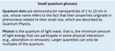
Featured paper: Quantum dots with unique rules.
[Paper: Evidence of Band-Edge Hole Levels Inversion in Spherical CuInS2 Quantum Dots. Gabriel Nagamine, Henrique B. Nunciaroni, Hunter McDaniel, Alexander L. Efros, Carlos H. de Brito Cruz, and Lazaro A. Padilha. Nano Lett., 2018, 18 (10), pp 6353–6359. DOI: 10.1021/acs.nanolett.8b02707]
Quantum dots with unique rules
 A paper led by Brazilian researchers has revealed surprising news about the rules that determine the energy levels of electrons in quantum dots of copper and indium disulphide (CuInS2,) which stand out in the family of quantum dots for being non-toxic. The work was recently reported in Nano Letters (impact factor of 12.08).
The results of the study, confirmed by experimental and theoretical methods, showed a situation in the structure of energy bands that had never before been observed in other materials.
.svg)
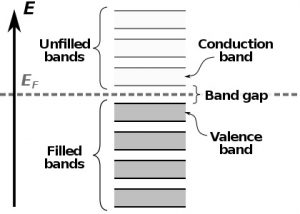
The band structure is a well-established scientific model that shows which energy states or levels the electrons can occupy in a given material. These states of energy are represented as allowed bands (those that the electrons can reach) and forbidden bands (those in which the electrons cannot be found).
In semiconductors, the energy bands that are allowed for an electron and that determine the properties of a material are the valence band and the conduction band. Both are separated by a band gap. For electrons to “jump” from the valence band to the conduction band, transposing the forbidden band in a process called transition, it is necessary they receive extra energy, which can occur when the material absorbs photons. When they lose energy, these electrons can once again occupy their places in the conduction band, and surplus energy can be emitted as photons (light). This light emission from the absorption of photons is known as photoluminescence.
Researchers at the Gleb Wataghin Institute of Physics at UNICAMP (Campinas, SP, Brazil) discovered that the quantum dots they were studying did not follow the same transition rules as other semiconductor materials and nanomaterials. “Generally, in semiconductors, bulk or nanostructured, the states that form the top of the valence band and the bottom of the conduction band are such that a transition between these states by absorption of a photon is allowed,” contextualizes Lázaro Aurélio Padilha Junior, professor at UNICAMP and corresponding author of the article. “What we showed was that in the studied material (CuInS2 quantum dots), this transition is forbidden by absorbing one photon. The interaction with two photons is required for this transition to occur. As far as we know, this is the first semiconductor system that presents this inversion of states,” says Padilha.
The discovery, besides showing that the norms that govern the electron states in semiconductors are not valid for all the materials, can influence the applications of the quantum dots studied. According to Padilha, the conditions discovered favor the simultaneous emission of two photons in the material when the electrons return to the conduction band. “This could be attractive to lasers systems that emit light in two distinct colors at the same time, and with color adjustment over a wide spectral range,” says the professor. In addition, adds Gabriel Nagamine, the first author of the article, understanding the structure of material bands can improve the performance of existing applications such as luminescent solar concentrators – a technology that can be used both to generate electricity from sunlight and to increase the production of food in greenhouses. “All these applications come from the unique characteristics of the electronic bands of these materials,” says Nagamine.
History of a theoretically announced experimental result
The history of this discovery goes back to 2015, when Professor Padilha, who has worked with quantum dots since 2010, his master’s student Gabriel Nagamine and other members of the research group decided to devote their efforts in studying the quantum dots of CuInS2. “This material caught our attention because it did not have heavy metals in its composition, which made it interesting for applications in biology and medicine, such as fluorescent biological markers,” says Padilha. In fact, quantum dots, which were discovered in the 1980s and are now present in products such as TV screens, present very interesting properties to be used in the detection of diseases and other applications in the health area, but almost all of them are toxic due to their chemical composition.
The UNICAMP team then collaborated with the company UbiQD, located in Los Álamos (USA) and specialized in the production of quantum dots, and which provided samples of spherical and pyramidal quantum dots. The characterization of the samples was performed partly in the company and also in the National Nanotechnology Laboratory (LNNano) of CNPEM, in the city of Campinas (SP, Brazil).
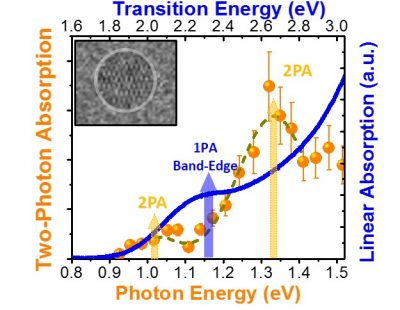
Initially, Padilha and his team set out to investigate how strong the absorption of two photons was in the chosen material, since this optical process allows to make three-dimensional images of the material, which can be very useful in its characterization and also in its application in several areas. To do this, in early 2016, the team performed the main experiments of the work at UNICAMP using a spectroscopy technique that allows detecting light emission from the absorption of two photons. “The first measurements revealed an absorption peak of two photons at smaller energies than those of linear absorption – a fact never previously observed experimentally,” Padilha says. “We believed it was a problem in our laser source and we repeated the experiment, achieving the same results,” he adds. These results, which are shown in the figure to the side, have arisen from the experiments performed with spherical quantum dots. In the pyramid-shaped quantum dot samples, the predominance of of two-photon absorption was not observed.
In May of the same year Padilha met with Dr. Alexander Efros (Naval Research Laboratory, USA) at a conference in South Korea. “He, who is one of the most respected theorists working on the electronic structure of semiconductor quantum dots, mentioned that he had made calculations that predicted a reversal in parity of states in these nanomaterials. We immediately noticed that I had proven his theory, “says Prof. Padilha. After that, they began working together and trying to understand other aspects of the problem, until they submitted the article to Nano Letters. The paper was accepted in less than two months.
The research that originated the paper is part of Gabriel Nagamine’s master’s thesis, defended in 2017 at UNICAMP, and received financial support from Brazilian research agencies (FAPESP and federal CNPq), the student support service (SAE) of UNICAMP and the Office of Naval Research (USA).
(Português) Seleção de professores pesquisadores para o PPGCEM – UNESC.
XVIII B-MRS Meeting: plenary lectures and memorial lecture.
XVIII B-MRS Meeting (Balneário Camboriú, SC, Brazil, September 22 – 26, 2019).
![]() Memorial Lecture
Memorial Lecture
Prof. Yvonne Primerano Mascarenhas
Instituto de Física de São Carlos – USP
Plenary Lectures
Prof. Julia Greer
California Institute of Technology – USA
Title: Materials by Design: Three-Dimensional Nano-Architected Meta-Materials
Prof. Stefano Baroni
Scuola Internazionale Superiore di Studi Avanzati – Italy
Title: Multi scale simulation of the color optical properties of natural dyes in solution
Prof. Alan Taub
University of Michigan – USA
Title: Challenges in Processing of Materials to Reduce Weight of Structural Components
Prof. Norbert Koch
Humboldt-Universität zu Berlin – Germany
Title: Hybrid inorganic/organic semiconductor structures for opto-electronics
Prof. Mingzhong Wu
Colorado State University – USA
Title: Spin Transfer in Topological Insulator/Magnetic Insulator Bi-Layered Structures
Prof. Maurizio Prato
Università degli Studi di Trieste – Italy
Title: Multifunctional Hybrid Carbon Interfaces