
[Original paper: Preservation of pristine Bi2Te3 thin film topological insulator surface after ex situ mechanical removal of Te capping layer. C. I. Fornari, P. H. O. Rappl, S. L. Morelhão, T. R. F. Peixoto, H. Bentmann, F. Reinert, and E. Abramof. APL Materials, volume 4, issue 10 (2016). doi 10.1063/1.4964610. Link para o artigo: http://aip.scitation.org/doi/full/10.1063/1.4964610]
Adhesive tape to help unlock secrets of topological insulators
A study led by researchers at the National Institute for Space Research (INPE) has made a very useful contribution to further advance the understanding of topological insulators, discovered over a decade ago, with promising characteristics to be used in quantum computers and in other applications. The research was reported in a paper recently published in the journal APL Materials.
The research idea began in 2009, when it was confirmed and published that bismuth telluride (Bi2Te3) is a three-dimensional topological insulator, that is, an insulating material with robust conductive states on the surface. Bismuth telluride had been theoretically predicted as a three-dimensional topological insulator in 2007. The experimental confirmation resulted from the observation of its surface topological states using a technique known as ARPES (angle-resolved photoemission).

The INPE research team then decided to study the properties of bismuth telluride using ARPES. They saw the possibility of starting the research with an equipment available at the Associated Laboratory of Sensors and Materials (LAS) of INPE, which could be used to begin investigations on the manufacturing of topological insulators without requiring new investments. “The Molecular Beam Epitaxy (MBE) equipment installed in LAS/INPE is dedicated to the growth of IV-VI compounds and has a source charged with Bi2Te3 alloys, which is used to dope these compounds,” explains Celso Israel Fornari, the corresponding author of the APL Materials article.
The work was performed in Fornari’s doctorate, started in 2013 and still underway, under the guidance of the researchers Eduardo Abramof and Paulo Henrique de Oliveira Rappl, and with funding from Brazilian agencies CNPq (federal) and FAPESP (São Paulo State).
The team knew that in order to analyze the samples, they would have to overcome a challenge intrinsic in topological insulators: in contact with air, the surface of these materials rapidly oxidizes, changing its properties and preventing to perform surface analyzes, fundamental to confirm the topological conductive states. Faced with this limitation, only in situ analyses could be carried out (those made in the manufacturing environment, in this case by coupling, through ultra-high vacuum lines, a surface characterization system to the manufacturing system). However, the situ analyses, besides limiting the possibilities to study the material, were not viable within the doctoral work of Celso Fornari, since he would conduct the measurements using ARPES, in Germany, at the University of Würzburg.
![Cross-section SEM-FEG image of a bismuth telluride sample protected with an amorphous tellurium cover. Adapted from the image of the APL Mat article [http://aip.scitation.org/doi/full/10.1063/1.4964610] under license CC BY 4.0 [https://creativecommons.org/licenses/by/4.0]](http://sbpmat.org.br/site/wp-content/uploads/2017/01/MEV_eng.jpg)
Therefore, the team had to develop a method to protect the surface of the topological insulator, while ensuring the integrity of the samples. The technique developed by the INPE researchers consists of depositing, at room temperature, a layer of amorphous tellurium, soon after the growth of the bismuth telluride.
In the first stage of the project, the team carefully fabricated bismuth telluride films with thickness ranging from 8 to 170 nm, and coated some of them with amorphous tellurium protective layers of 100-200 nm in thickness. The samples were characterized by various experimental techniques to analyze the substrates, films and protective layers. In particular, the INPE team, together with Professor Luiz Morelhão, from the Physics Institute of USP, analyzed the structure of the samples by X-ray diffraction in the Brazilian Synchrotron Light Laboratory (LNLS). Morelhão also collaborated with the INPE team in developing a computational model to simulate the X-ray diffraction curves. “These analyses were fundamental to identify the optimal growth conditions of bismuth telluride,” adds Fornari.
Secondly, the team faced yet another challenge in developing the film protection method. In fact, in Germany, the protective layer had to be removed from the samples without distorting the topological insulation in order to perform the surface analysis. Following a method that was already practiced by other scientists, the INPE researchers first planned to sublimate the protective layer within the ultra-high vacuum environment of the ARPES equipment.

In this procedure, the sample is adhered to a sample holder and an adhesive tape is attached to the protective layer. Removal can be done by pulling the tape or by moving the sample holder, as shown in the diagram on the right.
The method of deposition and subsequent removal of the protective layer developed by INPE team worked extremely well. The tellurium protective layer preserved the bismuth telluride samples from oxidation and contamination for about three months during their oceanic and terrestrial trip. The removal of the layer with adhesive tape, performed inside the ultra-high vacuum chamber of the ARPES equipment, was carried out without generating any distortions in the thickness, morphology or composition of the films, and consequently in their properties.
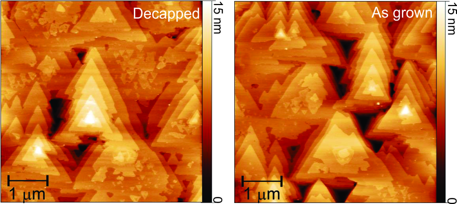
“This was the first experimental observation of bismuth telluride films with intrinsic insulating behavior analyzed ex situ,” remarks Fornari. “To date only films with intrinsic insulating behavior and grown within the same vacuum system (in situ) have been reported,” he states.
According to Fornari, the results obtained in relation to the method of deposition and removal of the protective layer indicate that it could be applied to other topological insulating materials, besides the bismuth telluride. Good news to those studying these materials, very promising for quantum computing and spintronics, keen to advance their understanding about these properties, which gained prominence in 2016 with the Nobel Prize in Physics. Good news also for society in general, which will probably benefit from their applications.