
[Paper: Gate-tunable non-volatile photomemory effect in MoS2 transistors. Andreij C Gadelha, Alisson R Cadore, Kenji Watanabe, Takashi Taniguchi, Ana M de Paula, Leandro M Malard, Rodrigo G Lacerda and Leonardo C Campos. 2D Materials, Volume 6, Number 2. DOI: 10.1088/2053-1583/ab0af1]
A scientific team from the Physics Department of the Brazilian Federal University of Minas Gerais (UFMG) developed a device based on ultrafine nanomaterials capable of recording and reading data, acting as computational memory. This memory, whose data storage mechanism originates based on optical phenomena – which is why it is called photo-memory – has shown to possess several of the characteristics currently desirable for memories: possibility of miniaturization, low power consumption, long data retention and relatively low cost.
The work opens up possibilities for developing efficient memories based on two-dimensional materials (those whose thickness is one or a few atoms) that could be used on lightweight and flexible platforms, such as wearable electronic devices. The research was reported in a recently published article in the scientific journal 2D Materials (impact factor 7,042).
“Our work consists of a scientific investigation with probable technological implications in the area of photo memories,” contextualizes Professor Leonardo Cristiano Campos (UFMG), corresponding author of the paper. “We developed a simple optoelectronic device, in which the simultaneous application of light and electrical charges modifies the electronic properties of molybdenum disulphide (MoS2), which is an ultrafine nanometric material,” he adds.

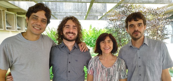
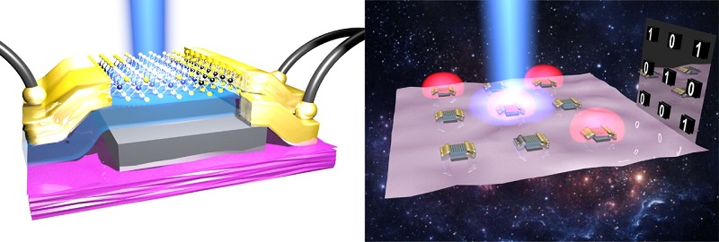
Initially, the doctoral students Andreij de Carvalho Gadelha and Alisson Cadore integrated a series of nanomaterials of few tens of nanometers in thickness, following the architecture of the field effect transistor (FET), which can be used as an electronic component of memories. The FET assembled at UFMG consists in essence of a layer of molybdenum disulfide placed on a flat crystal of hexagonal boron nitride, placed on a fine graphite substrate. Boron nitride was supplied by a research group from Japan, from the National Institute of Materials Science (NIMS).
The team then carried out a series of optoelectronic measures designed by the doctoral students Andreij and his supervisors (Professors Leonardo Campos and Rodrigo Gribel Lacerda), assisted by two opticians, Professors Leandro Malard Moreira and Ana Maria de Paula – all from the Physics Department of UFMG.
In general terms, the team simultaneously applied electrical voltage and laser radiation to FET. This combined action systematically changes the density of the free charges that travel through the molybdenum disulphide (semiconductor material), controlling the electrical conductivity of the material (process called photogating). The change persisted after the laser and tension were removed.
Thus, the scientific team generated in the material what is required to record data in digital electronics: two well-differentiated states that can be quickly detected and translated into the binary code such as zero (0) and one (1). Specifically, these are two states of conductivity of molybdenum disulphide: the one prior to the application of the laser light, called “off” or “0”, and the one subsequent to irradiation, called “on” or “1”, (this one characterized by the presence of the photocurrent).
In addition to revealing the ability of molybdenum disulphide FET to act as a photo-memory, the experiments and theoretical modeling performed at UFMG unveiled some very desirable characteristics in a memory: low power consumption (related to the ratio of “on” and “off”), and the ability to retain recorded data for long periods (the team estimated that up to 50% of a recorded data would remain saved after a decade).
The photo memory developed at UFMG demonstrated another interesting feature. By controlling the charge applied to FET, it is possible to modulate the conductivity states and generate a series of well-differentiated states (not only two).
“We believe that these memories can be applied in the long term,” says Professor Campos. To do this, says the scientist, it would be necessary to develop the large-scale production of nanomaterials, a challenge he estimates could be solved in a decade. In addition, it would require adapting the memory to the operation under environmental conditions, since the measurements carried out by the UFMG team were made in a vacuum. “We are developing encapsulation techniques that are likely to solve this issue,” says Campos.
The results reported in the 2D Materials article are part of Andreij Gadelha’s doctorate, who will defended his thesis on May 3. However, far from initially being chosen as a doctoral research subject, the molybdenum disulphide photo-memory effect was unveiled to the doctoral student and his advisor unexpectedly, as is often the case in the process of scientific discovery. “As if you’re looking at a specific point, but there’s that insight that turns your attention to the right path and you shout “EUREKA,” elucidates Professor Campos. Specifically, the doctoral student was attempting to annihilate certain effects that were undesirable in the context of the initial research, when he realized that these effects would enable an application in optical memories, and persuaded his advisor to change the focus of the work. “It is interesting to see that the undesirable effect has become our “golden-egg hen” leading to a turnaround in the direction of our research,” comments Campos.
The work was funded by the Brazilian federal agencies Capes, CNPq, the INCT of Nanocarbon and the Minas Gerais state agency Fapemig.
Oiti De Paula
Aí está a prova de que as universidades públicas brasileiras, além de ensino de alta qualidade, produzem conhecimento através das pesquisas nelas realizadas.
Análises e argumentos rasos, feitos por pessoas despreparadas, não podem destruir nossas universidades públicas!!!
Muito orgulho desses pesquisadores, em especial Ana Maria de Paula, um ser humano fantástico e uma professora e pesquisadora exemplar!!!