The scientific paper by members of the Brazilian community on Materials research featured this month is: GeO2/Ge structure submitted to annealing in deuterium: Incorporation pathways and associated oxide modifications. Bom, N.M.; Soares, G.V.; Hartmann, S.; Bordin, A.; Radtke, C. Applied Physics Letters 105, 141605 (2014); DOI: 10.1063/1.4898062.
Clarifying the processing of germanium for applications in micro and nanoelectronics
Germanium (Ge) is one of the semiconductor materials listed as possible alternatives to silicon for applications in the micro and nanoelectronics industry. However, the processing of materials based in germanium, aiming to optimize its electric properties for these applications is still presented as a challenge to the science.
In this context, a research team from the Federal University of Rio Grande do Sul (UFRGS) investigated the heat treatment (annealing) of germanium structures in deuterium atmosphere (hydrogen isotope which allows the use of analytical techniques specified for its quantification). The results of the study were recently published in the renowned periodical Applied Physics Letters (APL).
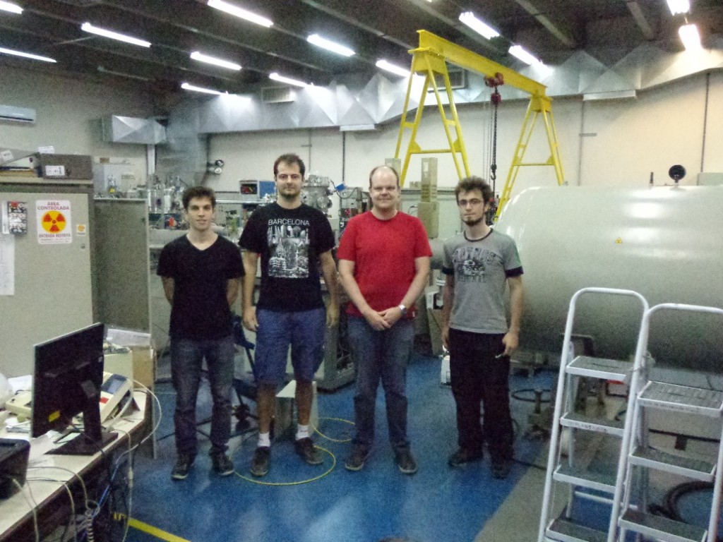
The study which the cited article derived from is part of the PhD research, in progress, by Nicolau Molina Bom, supervised by Professor Claudio Radtke in the framework of the postgraduate program in Microelectronics from UFRGS. “This work came up as a sequency of studies developed during my Masters, involving systems of aluminium oxide on germanium (Al2O3/Ge)”, Nicolau reports.
In the Masters’ research, also supervised by Radtke, Bom observed that the deposition of dielectric materials on germanium substrates, as well as its processing by means of heat treatment, induces the semiconductor oxidation and the formation of zirconium dioxide (GeO2). Due to reactions that occur between the oxide that is formed and the germanium substrate, the structure causes physical and chemical changes which bring about the degradation of its electric properties. “Thus, it became clear that the understanding of these mechanisms was fundamental to the use of germanium in industrial applications”, says Bom.
Incorporation of hydrogen
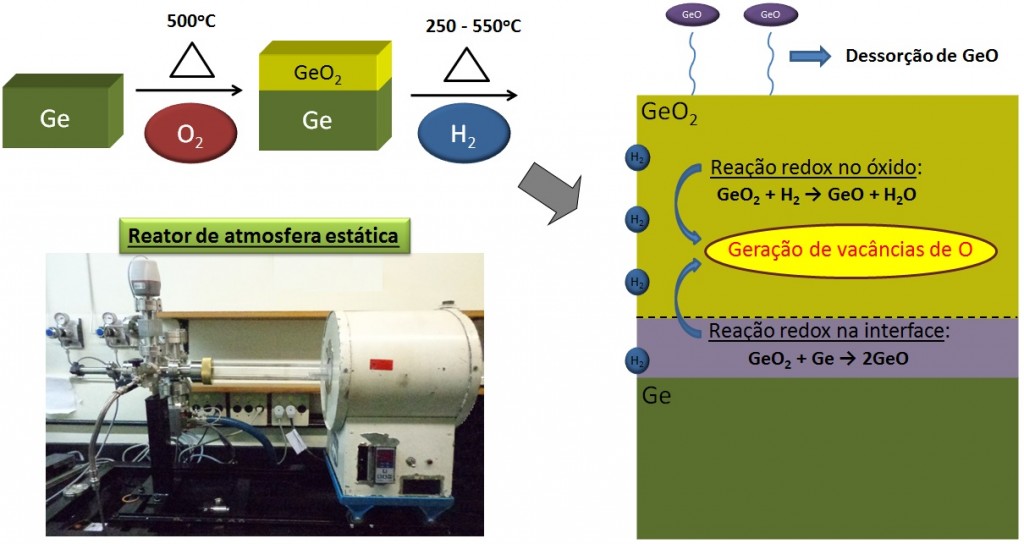
In the article published in APL, the authors report that the heat treatment was carried out in samples of germanium oxide on germanium (GeO2/Ge), of germanium oxide on silicon (GeO2/Si) and of silicon dioxide on silicon (SiO2/Si). One of the effects of the treatment evinced by means of analysis was the hydrogen incorporation, to greater proportions in GeO2/Ge than in SiO2/Si.
Authors assigned this effect to the occupation by hydrogen atoms of oxygen vacancies (points of crystalline network in which there are “vacancies” in the place of atoms that would be expected to be there), brought about during the heat treatment, in the interior of the germanium dioxide and in the GeO2/Ge interface.
Another effect observed by scientists was the oxide layer volatilization, mainly at temperatures superior to 450 oC, leading to changes in the chemical structure of the remaining oxide layer.
Schematic representation of the main results of the article, sent by Nicolau Bom.
Contribution and work applications
“The greatest merit of our study consists in clarifying the physical and chemical process involved in the incorporation of hydrogen in GeO2/Ge structures”, evaluates Nicolau Bom, who is the corresponding author of the article. “Besides, the understanding of these interactions will have a key role in the choice of the appropriate processing parameters in industrial applications involving germanium”, adds him.
In fact, results of this study can be applied, for example, in the development of metal oxide semiconductor field-effect transistors (MOSFET) based in germanium structures. “The MOSFET is the “flagship” of the micro/nanoelectronics industry and is a reference for the Moore’s law”remarks Bom. However, according to the PhD Candidate, the results presented in the cited article can also be useful in manufacturing devices with innovative architectures, such as the quantum well field-effect transistor (QWFET). “The high performance presented by QWFETs – due to the high mobilities obtained by the quantum confinement – set this device as a promising alternative to overcome the physical limitations of the conventional MOSFETs”, states Bom.
The study that the APL article derived from was funded by the INCT Namitec, INCT of Surface Engineering, CNPq, CAPES and FAPERGS.
Physics, Chemistry, Surface Science and Micro/nanoelectronics
The APL article inserts itself in a greater context of research, in the group of “Physical-chemistry of solid surfaces and interfaces” (FQSSI) at UFRGS. The central idea that guides this work is to understand the physical-chemical mechanisms involved in alternative materials to the classic structure SiO2/Si, in such a way to overcome the limitations of the silicon-based nanoelectronics . “In this context, the interdisciplinarity between physics, chemistry and engineering is a natural consequence of this work, where the knowledge derived from the different fields of study complement each other in the investigation of these systems”, remarks him.
Besides the studies about germanium, the group counts on works developed around dielectrics which door has high dielectric constant (the so-called high-k), SiC (material oriented to applications in extreme conditions of temperature, voltage and frequency) and graphene.


