
[Text by Christoph Deneke, Leonarde do Nascimento Rodrigues and Angelo Malachias, co-authors of the research, with editorial changes by B-MRS Newsletter.]
Changing material properties like the optical ones or the ability to conduct current by straining the material has a long tradition in semiconductor technology. Therefore, researchers have used this mechanism to control fundamental properties of different materials and discover new possibilities for technological application. In this regard, thin, nanometer thick membranes of semiconductor materials are especially well suited as they become extremely compliant and flexible due to being thin. Until now, such engineering was done by applying an external strain to ultra-thin membranes successfully changing fundamental properties like the band structure (the energy level distribution of the electrons inside the material).
A team of researchers from Brazilian universities demonstrated now that they can fundamentally change the optical properties of a semiconductor namomembrane, if they integrated it into a curved system, or in a tubular structure (rolled-up microtube). For this, the authors used a well established technology of releasing a strained layer system, which then self-assembles into a three-dimensional structure, in this case a rolled-up tube.
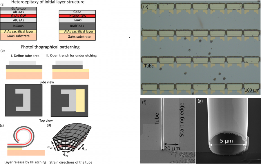
The way the nanostructures are made is illustrated in the image above. Initially, the team growth first a single crystal compromised of different materials. In following steps, they defined a U-shaped pattern on the surface of the structure by carrying out photolitography – the same kind of technology used to make computer chips. For the last step, that is responsible to form the final geometry in the form of a tube, they selectively removed a sacrificial layer previously introduced below the layers of interest. The schematics on the left of Fig. 1(a-d) represent the different steps of the tube fabrication. The optical microscopy image on the right together with the electron microscopy images (Fig. 1 f-g) depict the obtained structures.
“I am working since 2001 with these kind of systems. We already know that the properties of embedded quantum light sources change by the rolling-up. But until now, we used materials that were less affected by the geometrical change” tells Prof. Ch. Deneke from Unicamp. His long-time collaborator Prof. A. Malachias adds, “By using InGaAs instead of GaAs, we were able to achieve a complete change of the electronic structure of the material and the quantum light source integrated into the tube wall. The control of the band structure shown in the work is of great technological interest in the field of optical devices.” To investigate these changes, the team carried out optical measurements at Unicamp together with Prof. O. Couto Jr. and Prof. F. Iikawa. When using optical spectroscopy techniques to measure the polarization of light (the vibration plane of the light), the authors discovered that the optical response pointed to fundamental changes of the light source.
The image below shows the spectrum obtained by a reference structure (in its planar form) and in its new rolled-up form.
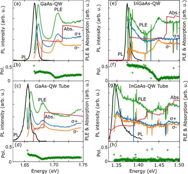
“With the vanishing of any polarization of the rolled-up layers, which included an InGaAs layer, we understood that the electronic structure and the optical properties had undergone fundamental changes. And we achieved this without relying on the application of an external force to control the expansion and compression of the material. The self-formation of these tubular structures is an elegant way to induce a hybrid state of compression and expansion, which in turn induces new effects”, explains Prof. L. N. Rodrigues, who worked in his postdoc together with Prof. Ch. Deneke on the system. Theoretical calculations show that the effect can be expected for all kind of curved systems made into tubes based on the used material system.
InGaAs and GaAs quantum light sources are already used. Basically, all lasers used in fiber communication are based on this material class, building the backbone of the internet communication unbeknownst to most people. Taking this into account, the light sources manufactured with the mentioned material, whose properties can be altered and controlled, are of great interest for the next generation of technology development, which includes, for example, quantum information or quantum computing. The fact that these tube-shaped semiconductor structures can be transformed into a light-emitting device (laser), together with the ability to alter and control physical properties without the need for any external voltage source, provide modern engineering that points in the direction of potential applications regarding light emitters and other fields of science. Furthermore, the results are also transferable to other semiconductor materials. Most important, this could be a model to modify Si (the most important material of the IT technology) in a similar way.
The work was largely supported by Brazilian agencies FAPESP and CNPq. The samples were grown and processed at LNNano / CNPEM, Campinas. X-ray diffraction measurements were carried out at the National Synchrotron Light Laboratory LNLS / CNPEM, Campinas. The optical spectroscopy measurements were performed at the GPO of the Physics Institute “Gleb Wataghin“ of Unicamp, Campinas.

Paper: Rolled-Up Quantum Wells Comprised of Nanolayered InGaAs/GaAs Heterostructures as Optical Materials for Quantum Information Technology. Leonarde N. Rodrigues, Diego Scolfaro, Lucas da Conceição, Angelo Malachias, Odilon D. D. Couto Jr., Fernando Iikawa, Christoph Deneke. ACS Applied Nano Materials 2021, DOI: 10.1021/acsanm.1c00354. Disponível na modalidade de acesso aberto em https://pubs.acs.org/doi/10.1021/acsanm.1c00354.
Corresponding author: Prof Chistoph Deneke (UNICAMP) – cdeneke@ifi.unicamp.br.